EP2084574B1 - Transparente schicht mit hoher elektrischer leitfähigkeit mit metallgitter mit optimiertem elektrochemischem widerstand - Google Patents
Transparente schicht mit hoher elektrischer leitfähigkeit mit metallgitter mit optimiertem elektrochemischem widerstand Download PDFInfo
- Publication number
- EP2084574B1 EP2084574B1 EP07858646.8A EP07858646A EP2084574B1 EP 2084574 B1 EP2084574 B1 EP 2084574B1 EP 07858646 A EP07858646 A EP 07858646A EP 2084574 B1 EP2084574 B1 EP 2084574B1
- Authority
- EP
- European Patent Office
- Prior art keywords
- layer
- grid
- glazing
- oxide
- doped
- Prior art date
- Legal status (The legal status is an assumption and is not a legal conclusion. Google has not performed a legal analysis and makes no representation as to the accuracy of the status listed.)
- Not-in-force
Links
Images

Classifications
-
- G—PHYSICS
- G02—OPTICS
- G02F—OPTICAL DEVICES OR ARRANGEMENTS FOR THE CONTROL OF LIGHT BY MODIFICATION OF THE OPTICAL PROPERTIES OF THE MEDIA OF THE ELEMENTS INVOLVED THEREIN; NON-LINEAR OPTICS; FREQUENCY-CHANGING OF LIGHT; OPTICAL LOGIC ELEMENTS; OPTICAL ANALOGUE/DIGITAL CONVERTERS
- G02F1/00—Devices or arrangements for the control of the intensity, colour, phase, polarisation or direction of light arriving from an independent light source, e.g. switching, gating or modulating; Non-linear optics
- G02F1/01—Devices or arrangements for the control of the intensity, colour, phase, polarisation or direction of light arriving from an independent light source, e.g. switching, gating or modulating; Non-linear optics for the control of the intensity, phase, polarisation or colour
- G02F1/15—Devices or arrangements for the control of the intensity, colour, phase, polarisation or direction of light arriving from an independent light source, e.g. switching, gating or modulating; Non-linear optics for the control of the intensity, phase, polarisation or colour based on an electrochromic effect
- G02F1/153—Constructional details
- G02F1/155—Electrodes
-
- B—PERFORMING OPERATIONS; TRANSPORTING
- B32—LAYERED PRODUCTS
- B32B—LAYERED PRODUCTS, i.e. PRODUCTS BUILT-UP OF STRATA OF FLAT OR NON-FLAT, e.g. CELLULAR OR HONEYCOMB, FORM
- B32B17/00—Layered products essentially comprising sheet glass, or glass, slag, or like fibres
- B32B17/06—Layered products essentially comprising sheet glass, or glass, slag, or like fibres comprising glass as the main or only constituent of a layer, next to another layer of a specific material
- B32B17/10—Layered products essentially comprising sheet glass, or glass, slag, or like fibres comprising glass as the main or only constituent of a layer, next to another layer of a specific material of synthetic resin
- B32B17/10005—Layered products essentially comprising sheet glass, or glass, slag, or like fibres comprising glass as the main or only constituent of a layer, next to another layer of a specific material of synthetic resin laminated safety glass or glazing
- B32B17/10009—Layered products essentially comprising sheet glass, or glass, slag, or like fibres comprising glass as the main or only constituent of a layer, next to another layer of a specific material of synthetic resin laminated safety glass or glazing characterized by the number, the constitution or treatment of glass sheets
- B32B17/10036—Layered products essentially comprising sheet glass, or glass, slag, or like fibres comprising glass as the main or only constituent of a layer, next to another layer of a specific material of synthetic resin laminated safety glass or glazing characterized by the number, the constitution or treatment of glass sheets comprising two outer glass sheets
-
- B—PERFORMING OPERATIONS; TRANSPORTING
- B32—LAYERED PRODUCTS
- B32B—LAYERED PRODUCTS, i.e. PRODUCTS BUILT-UP OF STRATA OF FLAT OR NON-FLAT, e.g. CELLULAR OR HONEYCOMB, FORM
- B32B17/00—Layered products essentially comprising sheet glass, or glass, slag, or like fibres
- B32B17/06—Layered products essentially comprising sheet glass, or glass, slag, or like fibres comprising glass as the main or only constituent of a layer, next to another layer of a specific material
- B32B17/10—Layered products essentially comprising sheet glass, or glass, slag, or like fibres comprising glass as the main or only constituent of a layer, next to another layer of a specific material of synthetic resin
- B32B17/10005—Layered products essentially comprising sheet glass, or glass, slag, or like fibres comprising glass as the main or only constituent of a layer, next to another layer of a specific material of synthetic resin laminated safety glass or glazing
- B32B17/1055—Layered products essentially comprising sheet glass, or glass, slag, or like fibres comprising glass as the main or only constituent of a layer, next to another layer of a specific material of synthetic resin laminated safety glass or glazing characterized by the resin layer, i.e. interlayer
- B32B17/1077—Layered products essentially comprising sheet glass, or glass, slag, or like fibres comprising glass as the main or only constituent of a layer, next to another layer of a specific material of synthetic resin laminated safety glass or glazing characterized by the resin layer, i.e. interlayer containing polyurethane
-
- G—PHYSICS
- G02—OPTICS
- G02F—OPTICAL DEVICES OR ARRANGEMENTS FOR THE CONTROL OF LIGHT BY MODIFICATION OF THE OPTICAL PROPERTIES OF THE MEDIA OF THE ELEMENTS INVOLVED THEREIN; NON-LINEAR OPTICS; FREQUENCY-CHANGING OF LIGHT; OPTICAL LOGIC ELEMENTS; OPTICAL ANALOGUE/DIGITAL CONVERTERS
- G02F1/00—Devices or arrangements for the control of the intensity, colour, phase, polarisation or direction of light arriving from an independent light source, e.g. switching, gating or modulating; Non-linear optics
- G02F1/01—Devices or arrangements for the control of the intensity, colour, phase, polarisation or direction of light arriving from an independent light source, e.g. switching, gating or modulating; Non-linear optics for the control of the intensity, phase, polarisation or colour
- G02F1/15—Devices or arrangements for the control of the intensity, colour, phase, polarisation or direction of light arriving from an independent light source, e.g. switching, gating or modulating; Non-linear optics for the control of the intensity, phase, polarisation or colour based on an electrochromic effect
- G02F1/153—Constructional details
- G02F1/1533—Constructional details structural features not otherwise provided for
- G02F2001/1536—Constructional details structural features not otherwise provided for additional, e.g. protective, layer inside the cell
-
- Y—GENERAL TAGGING OF NEW TECHNOLOGICAL DEVELOPMENTS; GENERAL TAGGING OF CROSS-SECTIONAL TECHNOLOGIES SPANNING OVER SEVERAL SECTIONS OF THE IPC; TECHNICAL SUBJECTS COVERED BY FORMER USPC CROSS-REFERENCE ART COLLECTIONS [XRACs] AND DIGESTS
- Y10—TECHNICAL SUBJECTS COVERED BY FORMER USPC
- Y10T—TECHNICAL SUBJECTS COVERED BY FORMER US CLASSIFICATION
- Y10T29/00—Metal working
- Y10T29/49—Method of mechanical manufacture
- Y10T29/49002—Electrical device making
- Y10T29/49117—Conductor or circuit manufacturing
- Y10T29/49124—On flat or curved insulated base, e.g., printed circuit, etc.
Definitions
- the subject of the present invention is an electroconductive layer for an electrochemical device, and / or electrically controllable of the glazing type and with variable optical and / or energy properties, or a photovoltaic device, or else an electroluminescent device. More particularly, it relates to a transparent layer with high electrical conductivity with a metal grid with optimized electrochemical resistance, suitable for undergoing heat treatment of the bending or quenching type.
- glazing may be the control of solar input through glazing mounted outdoors in buildings or vehicles of the car, train or plane type.
- the goal is to be able to limit excessive heating inside the interiors / premises, but only in case of strong sunshine.
- mirrors used as mirrors to punctually avoid the driver to be dazzled, or signs, so that messages appear when necessary, or intermittently to better attract attention. Glazing that can be rendered at will scattering can be used when desired as projection screens.
- glazing mounted in internal partitions in premises, trains, planes or mounted automotive side windows, or more particularly, when these windows are mounted in front of a flat screen type for example LCD, or plasma.
- the facade element usually a glass substrate, plays a predominant role in the aesthetics of the screen.
- the inventors came up with the idea of proposing to substitute for this lowered T L facade a transparent substrate provided with an electrically controllable system allowing such modifications of aesthetic appearance.
- electrochromic systems To modulate the light transmission and / or the thermal transmission of the glazings, there are also so-called electrochromic systems. These, in known manner, generally comprise two layers of electrochromic material separated by an electrolyte layer and framed by two electroconductive layers. Each of the layers of electrochromic material can reversibly insert cations and electrons, the modification of their degree of oxidation following these insertions / phasesinsertions leading to a change in its optical and / or thermal properties. We can notably modulate their absorption and / or their reflection in the wavelengths of the visible and / or infra-red.
- optical valves There are also systems called “optical valves". They are films comprising a generally crosslinked polymer matrix in which are dispersed micro-droplets containing particles which are capable of being placed in a preferred direction under the action of a magnetic or electric field. It is thus known from the patent WO93 / 09460 an optical valve comprising a polyorganosilane matrix and polyiodide-type particles which intercept much less light when the film is energized.
- liquid crystal systems a mode of operation similar to the previous ones. They are based on the use of a film placed between two conducting layers and based on a polymer in which liquid crystal droplets, in particular nematic with positive dielectric anisotropy, are arranged.
- the liquid crystals when the film is energized, are oriented along a preferred axis, which allows vision. When the crystals are not aligned, the film becomes diffused and prevents vision. Examples of such films are described in particular in European patents EP-0 238 164 , and Americans U.S. 4,435,047 , US-4,806,922 , US-4,732,456 . This type of film, once laminated and incorporated between two glass substrates, is marketed by Saint-Gobain Vitrage under the trade name "Priva-Lite".
- NCAP Nematic Curvilinearly Aligned Phases
- PDLC Polymer Dispersed Liquid Crystal
- cholesteric liquid crystal polymers such as those described in US Pat. WO92 / 19695 .
- electroluminescent systems they comprise a material or a stack of electroluminescent, organic or inorganic materials supplied with electricity by electrodes.
- electroconductive layers commonly comprise a layer based on indium oxide, generally tin-doped indium oxide better known under the abbreviation ITO. It may also be layers based on doped tin oxide, for example antimony, or based on doped zinc oxide, for example aluminum (or a mixture based on at least two of these oxides).
- ITO layers have been particularly studied. They can be easily deposited by magnetic field assisted sputtering, either from an oxide target (non-reactive sputtering), or from an indium and tin-based target (reactive sputtering in the presence of an oxidizing agent of the oxygen type). However, to present an electrical conductivity sufficient for the application and to be electrochemically robust, they require the use of a thermal treatment step in situ or recovery (often above 300 ° C).
- the ITO even annealed, has insufficient conductivity, inducing a pressure drop phenomenon during the changes of state of the system (transition of a colored state to a discolored state). This is reflected in the specific case of an electro-controlled system of electrochromic type by a inhomogeneous switching and linearly slow switching speed depending on the surface of the system. It will be understood that if an ITO-based electroconductive layer is used in an electrochromic system associated with a glass-function substrate as a flat screen façade element, the technical specifications of the ITO are incompatible with this type of use. (eg switching speed between the off state and the on state of the display).
- Another approach is to insert, in a stack of oxide layers, a metal layer to improve the surface resistance of the electroconductive layer This metal layer is otherwise thin enough to maintain a certain level of light transmission
- the document WO93 / 05438 an electroconductive layer consisting of a thin metal layer including silver, copper, aluminum which is associated with a layer based on a metal blocker such as iron, zirconium, titanium, tungsten .
- This TCO type: English abbreviation for "Conductive Transparent Oxide” is intended to be integrated into an electrochemical device of the electrochromic type in which the metal blocking layer constitutes a barrier to the diffusion of Li + ions between one of the active layers. and the metal layer.
- the document US2006 / 0033978 discloses an electrochemical layer with variable optical properties comprising a metal gate and an electrochemical protection layer.
- Another strategy for improving the electrochemical resistance of the metal layer is to protect it by the combination of two oxides ZnO: A1 and ITO (see the patent application FR 2886419 ).
- the aim of the invention is to obtain an assembly of electroconductive electrochemically robust layers and allowing fast switching times to form the electrodes of the electrochemical / electrocontrollable systems of the type previously described (electrochromics, photovoltaics, etc.). .
- it is a question of achieving this objective at a lower cost and by avoiding the heat treatment steps and without upsetting the known configurations of the electrochemical systems concerning the invention.
- It is, more generally, to develop electrodes on substantially transparent substrate (glass or polymer material), which are better.
- the subject of the invention is the electroconductive layer of claim 1.
- the term “lower” electrode means the electrode which is closest to the carrier substrate taken as reference, on which at least part of the active layers (for example all the active layers in a electrochromic system “all solid") is deposited.
- the “upper” electrode overcomes the stack of active layers, with respect to the same reference substrate.
- the lower electrode incorporating the electroconductive layer according to the invention has an electrical resistivity of between 0.2 and 0.6 Ohm / square and a TL of 75 to 85%, which makes its use as a transparent electrode perfectly satisfactory.
- the metal gate has a total thickness of between 1 and 3 ⁇ m,
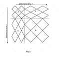
- the electrode remains transparent, that is to say that it has a low light absorption in the visible even in the presence of the grid (its network is almost invisible given its dimensions).
- the grid has a periodic or aperiodic structure representing a concealment of 15 to 25% of the light. For example, a square lattice having metallic strands 20 ⁇ m wide spaced apart from 300 ⁇ m gives a bare substrate of light transmission 92% a light transmission of 80%. Examples of realization of these periodic or aperiodic structures are described in the German application DE 10 2006 045 514.2
- the invention can be applied to different types of electrochemical or electrically controllable systems. It is more particularly interested in electrochromic systems, especially the "all solid” ones (the “all solid” being defined, within the meaning of the invention for stacks of layers for which all the layers are of inorganic nature) or the “all solid” polymer “(the” all polymer “being defined, within the meaning of the invention for stacks of layers for which all the layers are of organic nature), or for mixed electrochromic or hybrid (the layers of the stack are of organic nature and inorganic nature) or to liquid crystal or viologen systems, or electroluminescent systems.
- the electrochromic systems or glazing to which the invention can be applied are described in the aforementioned patents. They may comprise at least one carrier substrate and a stack of functional layers comprising at least successively a first electroconductive layer as previously described, an electrochemically active layer capable of reversibly inserting ions such as H + , Li + , OH- of the type anodic or cathodic electrochromic material, an electrolyte layer, a second electrochemically active layer capable of reversibly inserting ions such as H + , Li + , OH - of the cathodic or anodic electrochromic material type, and a second electroconductive layer, (the term "layer” is to be understood as a single layer or a superposition of several layers, continuous or discontinuous).
- the invention also relates to the incorporation of the electrochemical devices described in the preamble of the present application into glazings, operating in transmission.
- the term "glazing” is to be understood in the broad sense and includes any substantially transparent material, glass and / or polymeric material (such as polycarbonate PC or polymethyl methacrylate PMMA).
- the substrates carriers and / or counter-substrates that is to say the substrates surrounding the active system, can be rigid, flexible or semi-flexible.
- the invention also relates to the various applications that can be found in these devices, glazing or mirrors: it may be to make glazing for building, including external glazing, internal partitions or glass doors). It can also be windows, roofs or internal partitions of means of transport such as trains, planes, cars, boats, construction equipment. It can also be display screens or display, such as projection screens, television or computer screens, touch screens. They can also be used to make glasses or camera lenses, or to protect solar panels. They can also be used as energy storage devices of the battery type, fuel cell, batteries and batteries themselves.
- Example 1 The electrochromic device described above constitutes Example 1.
- Example 2 is given below which is a known structure of the prior art and for which both the lower and upper electrodes are based on ITO or SnO 2 : F
- the upper electrode has other conductive elements: it may be more particularly to associate the electrode to a more conductive layer that it, and / or a plurality of strips or son son.
- a preferred embodiment of this type of electrode consists in applying to the ITO layer (optionally surmounted by one or more other conductive layers) a network of conducting wires embedded in the surface of a polymer sheet (which may then protect the active system and / or allow the lamination of the glass-type carrier-substrate with another glass in the case of electroactive glazing production, of the electrochromic type, for example).
- the grid 9 made of aluminum can be obtained for example by a photolithography technique, or by a laser ablation technique and the values of TL are given below in Table 1 below. (light transmission) and electric conduction obtained. Thickness A1 ( ⁇ m) TL (%) Rc ( ⁇ / square) Laser grid 1 75-77 0.8 - 0.9 Laser grid 3 76 - 78 0.4 - 0.6 Litho grid 1 68 - 70 0.7 - 0.8 Litho grid 3 67 - 71 0.3 - 0.4
- the grid object of the invention is capable of undergoing heat treatments, in particular it resists bending or even quenching.
- an aluminum layer of approximately 3 ⁇ m After having deposited on a substrate with a glass function, for example by a magnetron sputtering method, an aluminum layer of approximately 3 ⁇ m, this layer being coated with a titanium nitride electrochemical protection layer of approximately 20 ⁇ m. nm, for example also deposited by magnetron sputtering.
- a barrier layer based on silicon nitride is interposed between the glass-function substrate and the aluminum-based metal layer.
- This stack is then etched by lithographic techniques, or laser ablation.
- the grid thus formed on a first substrate is associated with a second substrate against glass and so as to be located either on the face 2 or on the face 3 of the assembly constituted by the superposition of the two substrates.
- the bending of the two superposed sheets is carried out by any suitable method, in particular by gravity on supports such as skeletons, frames, by pressing and / or by suction on frames or solid forms.
- the grid thus formed is associated with a substrate which is quenched by any conventional soaking process.
- the nature of the stack from which the grid has been made is particularly suitable for resisting oxidation (aluminum passing), titanium nitride forming an oxidation barrier, the gate being also protected from the oxygen through the lamination.
- a 3 ⁇ m thick grid having a width 40 ⁇ m strand length and a 300 ⁇ m inter-strand space has a square resistivity of 0.3 ⁇ / square before heat treatment and a resistivity of 0.25 ⁇ / square after bending or quenching.
- the invention also relates to the substrate provided with at least one electrode of the type described above, independently of the electrical / electrochemical device into which it is incorporated or intended to be incorporated, as well as the electrode itself.
- this grid can be used as an active layer in an electrochemical device, and / or electrically controllable and with variable optical and / or energy properties, or a photovoltaic device, or else a light-emitting device, or still another heating device, or possibly a flat lamp device, an electromagnetic shielding device, or any other device requiring a conductive transparent layer.
- this grid can be positioned within an opening made in the windshield through which a camera lens or any other type of electronic device points, this opening being constantly free of condensation. made of the heating device (cf. figure 4 ).
- the grid may be deformed, stretched on its support so as to locally have electrical properties (conductivity) different from the adjacent zone.
Landscapes
- Physics & Mathematics (AREA)
- Nonlinear Science (AREA)
- General Physics & Mathematics (AREA)
- Optics & Photonics (AREA)
- Electrochromic Elements, Electrophoresis, Or Variable Reflection Or Absorption Elements (AREA)
- Laminated Bodies (AREA)
- Non-Insulated Conductors (AREA)
- Hybrid Cells (AREA)
Claims (11)
- Elektrochemische / elektrisch steuerbare Vorrichtung mit veränderlichen optischen und/oder energetischen Eigenschaften, umfassend wenigstens ein Trägersubstrat (S1), das mit einer elektroaktiven Schicht oder mit einem Stapel (3) von elektroaktiven Schichten, die/der zwischen einer sogenannten "unteren" Elektrode (2) und einer sogenannten "oberen" Elektrode (4) angeordnet ist, versehen ist, wobei wenigstens eine der unteren (2) oder oberen (4) Elektroden wenigstens eine elektrisch leitende Schicht umfasst, die von einem aus einem reinen Metall bestehenden Metallgitter (9) gebildet ist, dadurch gekennzeichnet, dass die Dicke des Gitters (9) im Bereich zwischen 1 und 15 µm und bevorzugter zwischen 2 und 8 µm liegt und noch bevorzugter nahe 3 µm beträgt, dass die elektrisch leitende Schicht mit wenigstens einer elektrochemischen Schutzschicht (10) auf der Basis eines Materials, das aus Titan, Gold, Platin, Palladium ausgewählt ist, überzogen ist, wobei das Material eventuell nitriert ist, und dass die elektrochemische Schutzschicht (10) wenigstens einer Sperrschicht (11) auf der Basis von Metalloxid zugeordnet ist, das aus Zinkoxid, Mischoxid aus Zink, das mit einem weiteren Metall, ausgewählt aus der Familie der folgenden Metalle: Al, Ga, B, Sc, dotiert ist, dotiertem Indiumoxid, insbesondere mit Zinn dotiertem, dotiertem Zinnoxid, insbesondere mit Antimon dotiertem, ausgewählt ist.
- Vorrichtung nach Anspruch 1, dadurch gekennzeichnet, dass das Gitter (9) auf der Basis eines reinen Materials besteht, das aus Silber, Kupfer, Zink, Aluminium, Nickel, Chrom, einer Nickel-Chrom-Legierung ausgewählt ist.
- Vorrichtung nach einem der vorhergehenden Ansprüche, dadurch gekennzeichnet, dass das Gitter (9) eine periodische oder aperiodische Struktur aufweist, die eine Abdeckung von 15 bis 25 % des Lichtes ausmacht.
- Vorrichtung nach einem der vorhergehenden Ansprüche, dadurch gekennzeichnet, dass die Dicke der elektrochemischen Schutzschicht (10) im Bereich zwischen 10 und 100 nm und bevorzugter zwischen 25 und 75 nm liegt und noch bevorzugter nahe 50 nm beträgt.
- Vorrichtung nach einem der vorhergehenden Ansprüche, dadurch gekennzeichnet, dass die Dicke der Sperrschicht (11) im Bereich zwischen 40 und 400 nm und bevorzugter zwischen 60 und 300 nm liegt und noch bevorzugter nahe 250 nm beträgt.
- Vorrichtung nach einem der vorhergehenden Ansprüche, dadurch gekennzeichnet, dass das Gitter (9) auf eine zweite Sperrschicht, insbesondere auf der Basis von Siliziumnitrid aufgebracht ist.
- Vorrichtung nach einem der vorhergehenden Ansprüche, dadurch gekennzeichnet, dass der spezifische Widerstand der elektrisch leitenden Schicht (2) im Bereich zwischen 0.01 Ohm/Quadrat und 1 Ohm/Quadrat, bevorzugt zwischen 0.2 und 0.6 Ohm/Quadrat liegt und noch bevorzugter nahe 0.4 Ohm/Quadrat beträgt.
- Vorrichtung nach einem der vorhergehenden Ansprüche, dadurch gekennzeichnet, dass das Gitter seine Eigenschaften elektrischer Leitfähigkeit vor und nach Wärmebehandlung bewahrt.
- Vorrichtung nach dem vorhergehenden Anspruch, dadurch gekennzeichnet, dass es sich um ein elektrochromes System, insbesondere ein elektrochromes "vollständig festes" System oder ein elektrochromes "vollständig festes" oder "vollständig polymeres" System, um ein Flüssigkristall-System oder um ein Viologen-System oder um ein Elektrolumineszenz-System handelt.
- Verglasung, dadurch gekennzeichnet, dass sie die Vorrichtung nach einem der vorhergehenden Ansprüche einschließt.
- Verwendung der Vorrichtung nach einem der Ansprüche 1 bis 9 oder der Verglasung nach Anspruch 10 zur Herstellung von Verglasungen für Gebäude, Verglasungen zur Ausstattung von Innentrennwänden oder Fenstern oder Dächern oder zur Ausstattung von Verkehrsmitteln vom Typ Flugzeug, Zug, Auto, Schiff, Baustellenfahrzeug, Bild- und Anzeigeschirme, wie Computer- oder Fernsehbildschirme oder Projektionsschirme, Touchscreens, zur Herstellung von Brillen oder von Objektiven für Fotoapparate oder von Schutzvorrichtungen für Solarpaneele oder von Leuchtflächen.
Applications Claiming Priority (3)
| Application Number | Priority Date | Filing Date | Title |
|---|---|---|---|
| FR0654708A FR2908228B1 (fr) | 2006-11-03 | 2006-11-03 | Couche transparente a haute conductivite electrique avec grille metallique a tenue electrochimique optimisee |
| FR0754333A FR2908229B1 (fr) | 2006-11-03 | 2007-04-05 | Couche transparente a haute conductivite electrique avec grille metallique a tenue electrochimique optimisee adaptee pour subir un traitement thermique de type bombage, ou trempe |
| PCT/FR2007/052226 WO2008053109A2 (fr) | 2006-11-03 | 2007-10-22 | Couche transparente a haute conductivite electrique avec grille metallique a tenue electrochimique optimisee |
Publications (2)
| Publication Number | Publication Date |
|---|---|
| EP2084574A2 EP2084574A2 (de) | 2009-08-05 |
| EP2084574B1 true EP2084574B1 (de) | 2014-09-24 |
Family
ID=39271686
Family Applications (1)
| Application Number | Title | Priority Date | Filing Date |
|---|---|---|---|
| EP07858646.8A Not-in-force EP2084574B1 (de) | 2006-11-03 | 2007-10-22 | Transparente schicht mit hoher elektrischer leitfähigkeit mit metallgitter mit optimiertem elektrochemischem widerstand |
Country Status (8)
| Country | Link |
|---|---|
| US (1) | US8411348B2 (de) |
| EP (1) | EP2084574B1 (de) |
| JP (1) | JP5675103B2 (de) |
| KR (1) | KR101479597B1 (de) |
| CA (1) | CA2668004A1 (de) |
| FR (1) | FR2908229B1 (de) |
| RU (1) | RU2468404C2 (de) |
| WO (1) | WO2008053109A2 (de) |
Families Citing this family (31)
| Publication number | Priority date | Publication date | Assignee | Title |
|---|---|---|---|---|
| JP4837957B2 (ja) * | 2005-08-23 | 2011-12-14 | 株式会社エヌ・ティ・ティ・ドコモ | 移動局、基地局および移動通信システムならびに通信方法 |
| FR2904123B1 (fr) * | 2006-07-21 | 2008-09-12 | Saint Gobain | Dispositif electrochimique / electrocommandable du type vitrage et a proprietes optiques et/ou energetiques variables. |
| FR2904704B1 (fr) * | 2006-08-04 | 2008-12-05 | Saint Gobain | Dispositif electrochimique, et/ou elelctrocommandable du type vitrage et a proprietes optiques et/ou energetiques variables |
| FR2928463B1 (fr) * | 2008-03-04 | 2010-12-03 | Saint Gobain | Dispositif electrochrome comportant un maillage. |
| FR2934062B1 (fr) * | 2008-07-17 | 2010-08-13 | Saint Gobain | Dispositif electrochrome a reflexion infrarouge controlee |
| FR2936361B1 (fr) * | 2008-09-25 | 2011-04-01 | Saint Gobain | Procede de fabrication d'une grille submillimetrique electroconductrice, grille submillimetrique electroconductrice |
| FR2956869B1 (fr) | 2010-03-01 | 2014-05-16 | Alex Hr Roustaei | Systeme de production de film flexible a haute capacite destine a des cellules photovoltaiques et oled par deposition cyclique des couches |
| JP2011191588A (ja) * | 2010-03-16 | 2011-09-29 | Ricoh Co Ltd | エレクトロクロミック表示装置及びその製造方法 |
| US8923014B2 (en) * | 2010-08-19 | 2014-12-30 | Lg Display Co., Ltd. | Display device having touch panel |
| KR101754329B1 (ko) | 2010-12-09 | 2017-07-06 | 삼성전자주식회사 | 전기 변색 소자 및 그 제조 방법 |
| KR101841618B1 (ko) | 2010-12-16 | 2018-03-23 | 삼성전자주식회사 | 전기 변색 소자용 잉크, 전기 변색 소자 및 그 제조 방법 |
| KR101519765B1 (ko) * | 2013-12-30 | 2015-05-12 | 현대자동차주식회사 | 무베젤 태양전지 어레이 방법 |
| US9988707B2 (en) | 2014-05-30 | 2018-06-05 | Ppg Industries Ohio, Inc. | Transparent conducting indium doped tin oxide |
| US11130195B2 (en) | 2014-07-29 | 2021-09-28 | Gentex Corporation | Laser ablation with reduced visual effects |
| CN106794553B (zh) | 2014-10-03 | 2020-01-07 | 金泰克斯公司 | 第二表面激光烧蚀 |
| CN108351564B (zh) | 2015-06-19 | 2020-10-09 | 金泰克斯公司 | 第二表面激光烧蚀 |
| US9927609B2 (en) | 2015-08-14 | 2018-03-27 | Gentex Corporation | Heads up display system |
| JP6886032B2 (ja) * | 2017-04-12 | 2021-06-16 | サン−ゴバン グラス フランス | 電気的に制御可能な光学特性を有する機能要素を含む複合ペイン |
| US11009760B2 (en) | 2017-05-05 | 2021-05-18 | Gentex Corporation | Interleaving laser ablation |
| US10575449B1 (en) * | 2017-06-19 | 2020-02-25 | Rockwell Collins, Inc. | Combined high frequency EMI shield and substrate heater using a thin film |
| CN111316159A (zh) | 2017-11-27 | 2020-06-19 | 金泰克斯公司 | 可切换偏振显示器 |
| CN111316160A (zh) | 2017-11-27 | 2020-06-19 | 金泰克斯公司 | 可切换偏振显示器 |
| CN110636941A (zh) * | 2018-04-23 | 2019-12-31 | 法国圣戈班玻璃厂 | 用于提高的鲁棒性的具有节段的长汇流排 |
| TWI725667B (zh) | 2018-12-28 | 2021-04-21 | 美商塞奇電致變色公司 | 形成電化學裝置之方法 |
| CN112748619A (zh) * | 2019-10-30 | 2021-05-04 | 传奇视界有限公司 | 变色玻璃 |
| CN112748617A (zh) * | 2019-10-30 | 2021-05-04 | 传奇视界有限公司 | 电致变色玻璃 |
| CN112817190A (zh) * | 2019-10-30 | 2021-05-18 | 传奇视界有限公司 | 变色玻璃 |
| CN112748618A (zh) * | 2019-10-30 | 2021-05-04 | 传奇视界有限公司 | 电致变色玻璃 |
| CN112745037A (zh) * | 2019-10-30 | 2021-05-04 | 传奇视界有限公司 | 电致变色玻璃制备方法 |
| CN112960912A (zh) * | 2019-12-14 | 2021-06-15 | 传奇视界有限公司 | 调光玻璃制备方法 |
| CN113555608B (zh) * | 2021-07-20 | 2023-02-28 | 南京大学 | 具有近零能耗显示器件的电化学系统、制备方法和显示方法 |
Family Cites Families (18)
| Publication number | Priority date | Publication date | Assignee | Title |
|---|---|---|---|---|
| JPS5756824A (en) * | 1980-09-24 | 1982-04-05 | Sharp Corp | Ecd display device |
| JP2503553B2 (ja) * | 1987-11-30 | 1996-06-05 | 凸版印刷株式会社 | エレクトロクロミック表示体 |
| US5124832A (en) * | 1989-09-29 | 1992-06-23 | Ppg Industries, Inc. | Laminated and sealed electrochromic window |
| FR2669122B1 (fr) * | 1990-11-14 | 1992-12-31 | Saint Gobain Vitrage Int | Vitrage electrochrome. |
| US5161048A (en) * | 1990-12-26 | 1992-11-03 | Ppg Industries, Inc. | Electrochromic window with metal grid counter electrode and acidic polyelectrolyte |
| US5293546A (en) * | 1991-04-17 | 1994-03-08 | Martin Marietta Corporation | Oxide coated metal grid electrode structure in display devices |
| FR2753545B1 (fr) * | 1996-09-18 | 1998-10-16 | Saint Gobain Vitrage | Dispositif electrochimique |
| US5923456A (en) * | 1997-12-19 | 1999-07-13 | Rockwell International Corporation | Reversible electrochemical mirror |
| US6317248B1 (en) * | 1998-07-02 | 2001-11-13 | Donnelly Corporation | Busbars for electrically powered cells |
| US6157480A (en) * | 1998-09-21 | 2000-12-05 | Gentex Corporation | Seal for electrochromic devices |
| FR2791147B1 (fr) * | 1999-03-19 | 2002-08-30 | Saint Gobain Vitrage | Dispositif electrochimique du type dispositif electrocommandable a proprietes optiques et/ou energetiques variables |
| US6914802B2 (en) * | 2000-02-11 | 2005-07-05 | Axon Technologies Corporation | Microelectronic photonic structure and device and method of forming the same |
| JP2002082360A (ja) * | 2000-09-11 | 2002-03-22 | Fuji Photo Film Co Ltd | 光書き込み型記録材料 |
| JP2002202527A (ja) * | 2000-12-28 | 2002-07-19 | Nec Corp | アクティブマトリクス型液晶表示装置 |
| FR2840078B1 (fr) * | 2002-05-22 | 2004-08-13 | Saint Gobain | Dispositif electrocommandable a proprietes optiques et/ou energetiques variables |
| JP2005086005A (ja) * | 2003-09-09 | 2005-03-31 | Seiko Epson Corp | 基板及びその製造方法並びに電気光学装置 |
| JP4569170B2 (ja) * | 2004-05-25 | 2010-10-27 | コニカミノルタホールディングス株式会社 | 表示素子及び複合電極の形成方法 |
| US7502156B2 (en) * | 2004-07-12 | 2009-03-10 | Gentex Corporation | Variable reflectance mirrors and windows |
-
2007
- 2007-04-05 FR FR0754333A patent/FR2908229B1/fr active Active
- 2007-10-22 RU RU2009121004/28A patent/RU2468404C2/ru not_active IP Right Cessation
- 2007-10-22 WO PCT/FR2007/052226 patent/WO2008053109A2/fr active Application Filing
- 2007-10-22 EP EP07858646.8A patent/EP2084574B1/de not_active Not-in-force
- 2007-10-22 CA CA002668004A patent/CA2668004A1/fr not_active Abandoned
- 2007-10-22 KR KR1020097008899A patent/KR101479597B1/ko not_active IP Right Cessation
- 2007-10-22 US US12/513,178 patent/US8411348B2/en active Active
- 2007-10-22 JP JP2009535105A patent/JP5675103B2/ja not_active Expired - Fee Related
Also Published As
| Publication number | Publication date |
|---|---|
| KR20090075850A (ko) | 2009-07-09 |
| FR2908229A1 (fr) | 2008-05-09 |
| RU2468404C2 (ru) | 2012-11-27 |
| JP2010508555A (ja) | 2010-03-18 |
| RU2009121004A (ru) | 2010-12-10 |
| US20100132988A1 (en) | 2010-06-03 |
| KR101479597B1 (ko) | 2015-01-07 |
| CA2668004A1 (fr) | 2008-05-08 |
| EP2084574A2 (de) | 2009-08-05 |
| FR2908229B1 (fr) | 2023-04-28 |
| WO2008053109A3 (fr) | 2008-06-26 |
| US8411348B2 (en) | 2013-04-02 |
| JP5675103B2 (ja) | 2015-02-25 |
| WO2008053109A2 (fr) | 2008-05-08 |
Similar Documents
| Publication | Publication Date | Title |
|---|---|---|
| EP2084574B1 (de) | Transparente schicht mit hoher elektrischer leitfähigkeit mit metallgitter mit optimiertem elektrochemischem widerstand | |
| EP1451634B1 (de) | Elektrode für elektrochemische und/oder elektrisch-steuerbare vorrichtungen | |
| EP2307926B1 (de) | Elektrochromes bauelement mit gesteuerter infrarotreflexion | |
| EP2047325B1 (de) | Elektrochemisch/elektrisch steuerbare glasvorrichtung mit veränderlichen optischen und/oder energetischen eigenschaften | |
| EP2263118B1 (de) | Elektrochrome vorrichtung mit zahnradeingriff | |
| WO2007000542A2 (fr) | Electrode de dispositifs electrochimiques/electrocommandables | |
| EP1952194B1 (de) | Elektrochromes system auf einem kunststoffsubstrat | |
| FR2904704A1 (fr) | Dispositif electrochimique, et/ou elelctrocommandable du type vitrage et a proprietes optiques et/ou energetiques variables | |
| WO2000057243A1 (fr) | Dispositif electrochimique, du type systeme electrocommandable a proprietes optiques et/ou energetiques variables | |
| EP2010384A1 (de) | Schichtverglasung und dichtung sowie umfangsverstärkungselemente dafür | |
| WO2012076799A1 (fr) | Dipositif electrochimique a proprietes de transmission optique et/ou energetique electrococommandables | |
| EP2201425A1 (de) | Verbesserungen an anzeigebildschirmen | |
| FR2908228A1 (fr) | Couche transparente a haute conductivite electrique avec grille metallique a tenue electrochimique optimisee | |
| WO2010004158A1 (fr) | Electrode isolante pour dispositif électrochimique |
Legal Events
| Date | Code | Title | Description |
|---|---|---|---|
| PUAI | Public reference made under article 153(3) epc to a published international application that has entered the european phase |
Free format text: ORIGINAL CODE: 0009012 |
|
| 17P | Request for examination filed |
Effective date: 20090415 |
|
| AK | Designated contracting states |
Kind code of ref document: A2 Designated state(s): AT BE BG CH CY CZ DE DK EE ES FI FR GB GR HU IE IS IT LI LT LU LV MC MT NL PL PT RO SE SI SK TR |
|
| RIN1 | Information on inventor provided before grant (corrected) |
Inventor name: VALENTIN, EMMANUEL Inventor name: LETOCART, PHILIPPE Inventor name: GIRON, JEAN-CHRISTOPHE Inventor name: DUBRENAT, SAMUEL Inventor name: JOUSSE, DIDIER Inventor name: KIM, SE-JONG Inventor name: STEERS, EMILIE |
|
| 17Q | First examination report despatched |
Effective date: 20091203 |
|
| DAX | Request for extension of the european patent (deleted) | ||
| GRAP | Despatch of communication of intention to grant a patent |
Free format text: ORIGINAL CODE: EPIDOSNIGR1 |
|
| INTG | Intention to grant announced |
Effective date: 20140415 |
|
| GRAS | Grant fee paid |
Free format text: ORIGINAL CODE: EPIDOSNIGR3 |
|
| GRAA | (expected) grant |
Free format text: ORIGINAL CODE: 0009210 |
|
| AK | Designated contracting states |
Kind code of ref document: B1 Designated state(s): AT BE BG CH CY CZ DE DK EE ES FI FR GB GR HU IE IS IT LI LT LU LV MC MT NL PL PT RO SE SI SK TR |
|
| REG | Reference to a national code |
Ref country code: GB Ref legal event code: FG4D Free format text: NOT ENGLISH |
|
| REG | Reference to a national code |
Ref country code: CH Ref legal event code: EP |
|
| REG | Reference to a national code |
Ref country code: AT Ref legal event code: REF Ref document number: 688868 Country of ref document: AT Kind code of ref document: T Effective date: 20141015 Ref country code: CH Ref legal event code: NV Representative=s name: KIRKER AND CIE S.A., CH |
|
| REG | Reference to a national code |
Ref country code: IE Ref legal event code: FG4D Free format text: LANGUAGE OF EP DOCUMENT: FRENCH |
|
| REG | Reference to a national code |
Ref country code: DE Ref legal event code: R096 Ref document number: 602007038694 Country of ref document: DE Effective date: 20141106 |
|
| REG | Reference to a national code |
Ref country code: SE Ref legal event code: TRGR |
|
| REG | Reference to a national code |
Ref country code: NL Ref legal event code: T3 |
|
| PG25 | Lapsed in a contracting state [announced via postgrant information from national office to epo] |
Ref country code: LT Free format text: LAPSE BECAUSE OF FAILURE TO SUBMIT A TRANSLATION OF THE DESCRIPTION OR TO PAY THE FEE WITHIN THE PRESCRIBED TIME-LIMIT Effective date: 20140924 Ref country code: FI Free format text: LAPSE BECAUSE OF FAILURE TO SUBMIT A TRANSLATION OF THE DESCRIPTION OR TO PAY THE FEE WITHIN THE PRESCRIBED TIME-LIMIT Effective date: 20140924 Ref country code: GR Free format text: LAPSE BECAUSE OF FAILURE TO SUBMIT A TRANSLATION OF THE DESCRIPTION OR TO PAY THE FEE WITHIN THE PRESCRIBED TIME-LIMIT Effective date: 20141225 |
|
| REG | Reference to a national code |
Ref country code: LT Ref legal event code: MG4D |
|
| PG25 | Lapsed in a contracting state [announced via postgrant information from national office to epo] |
Ref country code: CY Free format text: LAPSE BECAUSE OF FAILURE TO SUBMIT A TRANSLATION OF THE DESCRIPTION OR TO PAY THE FEE WITHIN THE PRESCRIBED TIME-LIMIT Effective date: 20140924 Ref country code: LV Free format text: LAPSE BECAUSE OF FAILURE TO SUBMIT A TRANSLATION OF THE DESCRIPTION OR TO PAY THE FEE WITHIN THE PRESCRIBED TIME-LIMIT Effective date: 20140924 |
|
| PG25 | Lapsed in a contracting state [announced via postgrant information from national office to epo] |
Ref country code: SK Free format text: LAPSE BECAUSE OF FAILURE TO SUBMIT A TRANSLATION OF THE DESCRIPTION OR TO PAY THE FEE WITHIN THE PRESCRIBED TIME-LIMIT Effective date: 20140924 Ref country code: EE Free format text: LAPSE BECAUSE OF FAILURE TO SUBMIT A TRANSLATION OF THE DESCRIPTION OR TO PAY THE FEE WITHIN THE PRESCRIBED TIME-LIMIT Effective date: 20140924 Ref country code: ES Free format text: LAPSE BECAUSE OF FAILURE TO SUBMIT A TRANSLATION OF THE DESCRIPTION OR TO PAY THE FEE WITHIN THE PRESCRIBED TIME-LIMIT Effective date: 20140924 Ref country code: RO Free format text: LAPSE BECAUSE OF FAILURE TO SUBMIT A TRANSLATION OF THE DESCRIPTION OR TO PAY THE FEE WITHIN THE PRESCRIBED TIME-LIMIT Effective date: 20140924 Ref country code: IS Free format text: LAPSE BECAUSE OF FAILURE TO SUBMIT A TRANSLATION OF THE DESCRIPTION OR TO PAY THE FEE WITHIN THE PRESCRIBED TIME-LIMIT Effective date: 20150124 Ref country code: PT Free format text: LAPSE BECAUSE OF FAILURE TO SUBMIT A TRANSLATION OF THE DESCRIPTION OR TO PAY THE FEE WITHIN THE PRESCRIBED TIME-LIMIT Effective date: 20150126 Ref country code: CZ Free format text: LAPSE BECAUSE OF FAILURE TO SUBMIT A TRANSLATION OF THE DESCRIPTION OR TO PAY THE FEE WITHIN THE PRESCRIBED TIME-LIMIT Effective date: 20140924 |
|
| PG25 | Lapsed in a contracting state [announced via postgrant information from national office to epo] |
Ref country code: PL Free format text: LAPSE BECAUSE OF FAILURE TO SUBMIT A TRANSLATION OF THE DESCRIPTION OR TO PAY THE FEE WITHIN THE PRESCRIBED TIME-LIMIT Effective date: 20140924 |
|
| REG | Reference to a national code |
Ref country code: DE Ref legal event code: R097 Ref document number: 602007038694 Country of ref document: DE |
|
| PG25 | Lapsed in a contracting state [announced via postgrant information from national office to epo] |
Ref country code: MC Free format text: LAPSE BECAUSE OF FAILURE TO SUBMIT A TRANSLATION OF THE DESCRIPTION OR TO PAY THE FEE WITHIN THE PRESCRIBED TIME-LIMIT Effective date: 20140924 |
|
| REG | Reference to a national code |
Ref country code: IE Ref legal event code: MM4A |
|
| PG25 | Lapsed in a contracting state [announced via postgrant information from national office to epo] |
Ref country code: DK Free format text: LAPSE BECAUSE OF FAILURE TO SUBMIT A TRANSLATION OF THE DESCRIPTION OR TO PAY THE FEE WITHIN THE PRESCRIBED TIME-LIMIT Effective date: 20140924 |
|
| PLBE | No opposition filed within time limit |
Free format text: ORIGINAL CODE: 0009261 |
|
| STAA | Information on the status of an ep patent application or granted ep patent |
Free format text: STATUS: NO OPPOSITION FILED WITHIN TIME LIMIT |
|
| 26N | No opposition filed |
Effective date: 20150625 |
|
| REG | Reference to a national code |
Ref country code: FR Ref legal event code: PLFP Year of fee payment: 9 |
|
| PG25 | Lapsed in a contracting state [announced via postgrant information from national office to epo] |
Ref country code: IE Free format text: LAPSE BECAUSE OF NON-PAYMENT OF DUE FEES Effective date: 20141022 |
|
| PGFP | Annual fee paid to national office [announced via postgrant information from national office to epo] |
Ref country code: LU Payment date: 20151021 Year of fee payment: 9 |
|
| PGFP | Annual fee paid to national office [announced via postgrant information from national office to epo] |
Ref country code: IT Payment date: 20151026 Year of fee payment: 9 Ref country code: CH Payment date: 20151012 Year of fee payment: 9 |
|
| PG25 | Lapsed in a contracting state [announced via postgrant information from national office to epo] |
Ref country code: SI Free format text: LAPSE BECAUSE OF FAILURE TO SUBMIT A TRANSLATION OF THE DESCRIPTION OR TO PAY THE FEE WITHIN THE PRESCRIBED TIME-LIMIT Effective date: 20140924 |
|
| PGFP | Annual fee paid to national office [announced via postgrant information from national office to epo] |
Ref country code: SE Payment date: 20151013 Year of fee payment: 9 Ref country code: NL Payment date: 20151012 Year of fee payment: 9 Ref country code: AT Payment date: 20150928 Year of fee payment: 9 Ref country code: BE Payment date: 20151028 Year of fee payment: 9 |
|
| PG25 | Lapsed in a contracting state [announced via postgrant information from national office to epo] |
Ref country code: BG Free format text: LAPSE BECAUSE OF FAILURE TO SUBMIT A TRANSLATION OF THE DESCRIPTION OR TO PAY THE FEE WITHIN THE PRESCRIBED TIME-LIMIT Effective date: 20140924 |
|
| PG25 | Lapsed in a contracting state [announced via postgrant information from national office to epo] |
Ref country code: HU Free format text: LAPSE BECAUSE OF FAILURE TO SUBMIT A TRANSLATION OF THE DESCRIPTION OR TO PAY THE FEE WITHIN THE PRESCRIBED TIME-LIMIT; INVALID AB INITIO Effective date: 20071022 Ref country code: MT Free format text: LAPSE BECAUSE OF FAILURE TO SUBMIT A TRANSLATION OF THE DESCRIPTION OR TO PAY THE FEE WITHIN THE PRESCRIBED TIME-LIMIT Effective date: 20140924 Ref country code: TR Free format text: LAPSE BECAUSE OF FAILURE TO SUBMIT A TRANSLATION OF THE DESCRIPTION OR TO PAY THE FEE WITHIN THE PRESCRIBED TIME-LIMIT Effective date: 20140924 |
|
| REG | Reference to a national code |
Ref country code: FR Ref legal event code: PLFP Year of fee payment: 10 |
|
| PG25 | Lapsed in a contracting state [announced via postgrant information from national office to epo] |
Ref country code: BE Free format text: LAPSE BECAUSE OF NON-PAYMENT OF DUE FEES Effective date: 20161031 |
|
| REG | Reference to a national code |
Ref country code: CH Ref legal event code: PL |
|
| REG | Reference to a national code |
Ref country code: NL Ref legal event code: MM Effective date: 20161101 |
|
| REG | Reference to a national code |
Ref country code: AT Ref legal event code: MM01 Ref document number: 688868 Country of ref document: AT Kind code of ref document: T Effective date: 20161022 |
|
| PG25 | Lapsed in a contracting state [announced via postgrant information from national office to epo] |
Ref country code: CH Free format text: LAPSE BECAUSE OF NON-PAYMENT OF DUE FEES Effective date: 20161031 Ref country code: LI Free format text: LAPSE BECAUSE OF NON-PAYMENT OF DUE FEES Effective date: 20161031 |
|
| PG25 | Lapsed in a contracting state [announced via postgrant information from national office to epo] |
Ref country code: SE Free format text: LAPSE BECAUSE OF NON-PAYMENT OF DUE FEES Effective date: 20161023 Ref country code: AT Free format text: LAPSE BECAUSE OF NON-PAYMENT OF DUE FEES Effective date: 20161022 Ref country code: NL Free format text: LAPSE BECAUSE OF NON-PAYMENT OF DUE FEES Effective date: 20161101 Ref country code: LU Free format text: LAPSE BECAUSE OF NON-PAYMENT OF DUE FEES Effective date: 20161022 |
|
| REG | Reference to a national code |
Ref country code: FR Ref legal event code: PLFP Year of fee payment: 11 |
|
| PG25 | Lapsed in a contracting state [announced via postgrant information from national office to epo] |
Ref country code: IT Free format text: LAPSE BECAUSE OF NON-PAYMENT OF DUE FEES Effective date: 20161022 |
|
| REG | Reference to a national code |
Ref country code: BE Ref legal event code: MM Effective date: 20161031 |
|
| REG | Reference to a national code |
Ref country code: FR Ref legal event code: PLFP Year of fee payment: 12 |
|
| PGFP | Annual fee paid to national office [announced via postgrant information from national office to epo] |
Ref country code: GB Payment date: 20210915 Year of fee payment: 15 |
|
| PGFP | Annual fee paid to national office [announced via postgrant information from national office to epo] |
Ref country code: DE Payment date: 20210914 Year of fee payment: 15 |
|
| PGFP | Annual fee paid to national office [announced via postgrant information from national office to epo] |
Ref country code: FR Payment date: 20211028 Year of fee payment: 15 |
|
| REG | Reference to a national code |
Ref country code: DE Ref legal event code: R119 Ref document number: 602007038694 Country of ref document: DE |
|
| GBPC | Gb: european patent ceased through non-payment of renewal fee |
Effective date: 20221022 |
|
| PG25 | Lapsed in a contracting state [announced via postgrant information from national office to epo] |
Ref country code: FR Free format text: LAPSE BECAUSE OF NON-PAYMENT OF DUE FEES Effective date: 20221031 Ref country code: DE Free format text: LAPSE BECAUSE OF NON-PAYMENT OF DUE FEES Effective date: 20230503 |
|
| PG25 | Lapsed in a contracting state [announced via postgrant information from national office to epo] |
Ref country code: GB Free format text: LAPSE BECAUSE OF NON-PAYMENT OF DUE FEES Effective date: 20221022 |