EP2083317A1 - Liquid crystal display and manufacturing method thereof - Google Patents
Liquid crystal display and manufacturing method thereof Download PDFInfo
- Publication number
- EP2083317A1 EP2083317A1 EP09151321A EP09151321A EP2083317A1 EP 2083317 A1 EP2083317 A1 EP 2083317A1 EP 09151321 A EP09151321 A EP 09151321A EP 09151321 A EP09151321 A EP 09151321A EP 2083317 A1 EP2083317 A1 EP 2083317A1
- Authority
- EP
- European Patent Office
- Prior art keywords
- transparent electrodes
- substrate
- liquid crystal
- crystal display
- photoresists
- Prior art date
- Legal status (The legal status is an assumption and is not a legal conclusion. Google has not performed a legal analysis and makes no representation as to the accuracy of the status listed.)
- Withdrawn
Links
- 239000004973 liquid crystal related substance Substances 0.000 title claims abstract description 66
- 238000004519 manufacturing process Methods 0.000 title claims description 20
- 239000000758 substrate Substances 0.000 claims abstract description 92
- 229920002120 photoresistant polymer Polymers 0.000 claims abstract description 75
- 125000006850 spacer group Chemical group 0.000 claims abstract description 73
- 238000000034 method Methods 0.000 claims abstract description 34
- 238000009413 insulation Methods 0.000 claims description 19
- 239000000463 material Substances 0.000 claims description 12
- 238000000059 patterning Methods 0.000 claims description 9
- 239000004988 Nematic liquid crystal Substances 0.000 claims 1
- 238000000206 photolithography Methods 0.000 abstract description 9
- 239000010408 film Substances 0.000 description 17
- 239000011521 glass Substances 0.000 description 10
- 239000011159 matrix material Substances 0.000 description 9
- XOLBLPGZBRYERU-UHFFFAOYSA-N tin dioxide Chemical compound O=[Sn]=O XOLBLPGZBRYERU-UHFFFAOYSA-N 0.000 description 9
- 230000015556 catabolic process Effects 0.000 description 5
- 238000006731 degradation reaction Methods 0.000 description 5
- 230000005684 electric field Effects 0.000 description 5
- VYPSYNLAJGMNEJ-UHFFFAOYSA-N Silicium dioxide Chemical compound O=[Si]=O VYPSYNLAJGMNEJ-UHFFFAOYSA-N 0.000 description 4
- 239000003513 alkali Substances 0.000 description 4
- 239000005388 borosilicate glass Substances 0.000 description 4
- 239000000203 mixture Substances 0.000 description 4
- 230000007935 neutral effect Effects 0.000 description 4
- 239000005361 soda-lime glass Substances 0.000 description 4
- 239000000126 substance Substances 0.000 description 4
- 239000011248 coating agent Substances 0.000 description 3
- 238000000576 coating method Methods 0.000 description 3
- AMGQUBHHOARCQH-UHFFFAOYSA-N indium;oxotin Chemical compound [In].[Sn]=O AMGQUBHHOARCQH-UHFFFAOYSA-N 0.000 description 3
- 239000007788 liquid Substances 0.000 description 3
- 229910001887 tin oxide Inorganic materials 0.000 description 3
- 229920000178 Acrylic resin Polymers 0.000 description 2
- 239000004925 Acrylic resin Substances 0.000 description 2
- VYZAMTAEIAYCRO-UHFFFAOYSA-N Chromium Chemical compound [Cr] VYZAMTAEIAYCRO-UHFFFAOYSA-N 0.000 description 2
- GWEVSGVZZGPLCZ-UHFFFAOYSA-N Titan oxide Chemical compound O=[Ti]=O GWEVSGVZZGPLCZ-UHFFFAOYSA-N 0.000 description 2
- 230000000903 blocking effect Effects 0.000 description 2
- 239000006229 carbon black Substances 0.000 description 2
- 238000005229 chemical vapour deposition Methods 0.000 description 2
- 229910052681 coesite Inorganic materials 0.000 description 2
- 238000007796 conventional method Methods 0.000 description 2
- 229910052906 cristobalite Inorganic materials 0.000 description 2
- 238000005530 etching Methods 0.000 description 2
- 238000002347 injection Methods 0.000 description 2
- 239000007924 injection Substances 0.000 description 2
- 230000003287 optical effect Effects 0.000 description 2
- 229920001721 polyimide Polymers 0.000 description 2
- 239000009719 polyimide resin Substances 0.000 description 2
- 239000011347 resin Substances 0.000 description 2
- 229920005989 resin Polymers 0.000 description 2
- 239000000377 silicon dioxide Substances 0.000 description 2
- 229910052682 stishovite Inorganic materials 0.000 description 2
- OGIDPMRJRNCKJF-UHFFFAOYSA-N titanium oxide Inorganic materials [Ti]=O OGIDPMRJRNCKJF-UHFFFAOYSA-N 0.000 description 2
- 229910052905 tridymite Inorganic materials 0.000 description 2
- 239000003086 colorant Substances 0.000 description 1
- 239000013078 crystal Substances 0.000 description 1
- 238000000151 deposition Methods 0.000 description 1
- 238000010586 diagram Methods 0.000 description 1
- 238000006056 electrooxidation reaction Methods 0.000 description 1
- 230000001939 inductive effect Effects 0.000 description 1
- 238000007645 offset printing Methods 0.000 description 1
- 230000003647 oxidation Effects 0.000 description 1
- 238000007254 oxidation reaction Methods 0.000 description 1
- 239000000049 pigment Substances 0.000 description 1
- 238000007650 screen-printing Methods 0.000 description 1
- 239000007787 solid Substances 0.000 description 1
- 239000002904 solvent Substances 0.000 description 1
- 239000010409 thin film Substances 0.000 description 1
Images




Classifications
-
- G—PHYSICS
- G02—OPTICS
- G02F—OPTICAL DEVICES OR ARRANGEMENTS FOR THE CONTROL OF LIGHT BY MODIFICATION OF THE OPTICAL PROPERTIES OF THE MEDIA OF THE ELEMENTS INVOLVED THEREIN; NON-LINEAR OPTICS; FREQUENCY-CHANGING OF LIGHT; OPTICAL LOGIC ELEMENTS; OPTICAL ANALOGUE/DIGITAL CONVERTERS
- G02F1/00—Devices or arrangements for the control of the intensity, colour, phase, polarisation or direction of light arriving from an independent light source, e.g. switching, gating or modulating; Non-linear optics
- G02F1/01—Devices or arrangements for the control of the intensity, colour, phase, polarisation or direction of light arriving from an independent light source, e.g. switching, gating or modulating; Non-linear optics for the control of the intensity, phase, polarisation or colour
- G02F1/13—Devices or arrangements for the control of the intensity, colour, phase, polarisation or direction of light arriving from an independent light source, e.g. switching, gating or modulating; Non-linear optics for the control of the intensity, phase, polarisation or colour based on liquid crystals, e.g. single liquid crystal display cells
- G02F1/133—Constructional arrangements; Operation of liquid crystal cells; Circuit arrangements
- G02F1/1333—Constructional arrangements; Manufacturing methods
- G02F1/1339—Gaskets; Spacers; Sealing of cells
- G02F1/13394—Gaskets; Spacers; Sealing of cells spacers regularly patterned on the cell subtrate, e.g. walls, pillars
-
- G—PHYSICS
- G02—OPTICS
- G02F—OPTICAL DEVICES OR ARRANGEMENTS FOR THE CONTROL OF LIGHT BY MODIFICATION OF THE OPTICAL PROPERTIES OF THE MEDIA OF THE ELEMENTS INVOLVED THEREIN; NON-LINEAR OPTICS; FREQUENCY-CHANGING OF LIGHT; OPTICAL LOGIC ELEMENTS; OPTICAL ANALOGUE/DIGITAL CONVERTERS
- G02F1/00—Devices or arrangements for the control of the intensity, colour, phase, polarisation or direction of light arriving from an independent light source, e.g. switching, gating or modulating; Non-linear optics
- G02F1/01—Devices or arrangements for the control of the intensity, colour, phase, polarisation or direction of light arriving from an independent light source, e.g. switching, gating or modulating; Non-linear optics for the control of the intensity, phase, polarisation or colour
- G02F1/13—Devices or arrangements for the control of the intensity, colour, phase, polarisation or direction of light arriving from an independent light source, e.g. switching, gating or modulating; Non-linear optics for the control of the intensity, phase, polarisation or colour based on liquid crystals, e.g. single liquid crystal display cells
- G02F1/133—Constructional arrangements; Operation of liquid crystal cells; Circuit arrangements
- G02F1/1333—Constructional arrangements; Manufacturing methods
- G02F1/1339—Gaskets; Spacers; Sealing of cells
-
- G—PHYSICS
- G02—OPTICS
- G02F—OPTICAL DEVICES OR ARRANGEMENTS FOR THE CONTROL OF LIGHT BY MODIFICATION OF THE OPTICAL PROPERTIES OF THE MEDIA OF THE ELEMENTS INVOLVED THEREIN; NON-LINEAR OPTICS; FREQUENCY-CHANGING OF LIGHT; OPTICAL LOGIC ELEMENTS; OPTICAL ANALOGUE/DIGITAL CONVERTERS
- G02F1/00—Devices or arrangements for the control of the intensity, colour, phase, polarisation or direction of light arriving from an independent light source, e.g. switching, gating or modulating; Non-linear optics
- G02F1/01—Devices or arrangements for the control of the intensity, colour, phase, polarisation or direction of light arriving from an independent light source, e.g. switching, gating or modulating; Non-linear optics for the control of the intensity, phase, polarisation or colour
- G02F1/13—Devices or arrangements for the control of the intensity, colour, phase, polarisation or direction of light arriving from an independent light source, e.g. switching, gating or modulating; Non-linear optics for the control of the intensity, phase, polarisation or colour based on liquid crystals, e.g. single liquid crystal display cells
- G02F1/133—Constructional arrangements; Operation of liquid crystal cells; Circuit arrangements
- G02F1/1333—Constructional arrangements; Manufacturing methods
- G02F1/1335—Structural association of cells with optical devices, e.g. polarisers or reflectors
- G02F1/133509—Filters, e.g. light shielding masks
- G02F1/133512—Light shielding layers, e.g. black matrix
-
- G—PHYSICS
- G02—OPTICS
- G02F—OPTICAL DEVICES OR ARRANGEMENTS FOR THE CONTROL OF LIGHT BY MODIFICATION OF THE OPTICAL PROPERTIES OF THE MEDIA OF THE ELEMENTS INVOLVED THEREIN; NON-LINEAR OPTICS; FREQUENCY-CHANGING OF LIGHT; OPTICAL LOGIC ELEMENTS; OPTICAL ANALOGUE/DIGITAL CONVERTERS
- G02F1/00—Devices or arrangements for the control of the intensity, colour, phase, polarisation or direction of light arriving from an independent light source, e.g. switching, gating or modulating; Non-linear optics
- G02F1/01—Devices or arrangements for the control of the intensity, colour, phase, polarisation or direction of light arriving from an independent light source, e.g. switching, gating or modulating; Non-linear optics for the control of the intensity, phase, polarisation or colour
- G02F1/13—Devices or arrangements for the control of the intensity, colour, phase, polarisation or direction of light arriving from an independent light source, e.g. switching, gating or modulating; Non-linear optics for the control of the intensity, phase, polarisation or colour based on liquid crystals, e.g. single liquid crystal display cells
- G02F1/133—Constructional arrangements; Operation of liquid crystal cells; Circuit arrangements
- G02F1/1333—Constructional arrangements; Manufacturing methods
- G02F1/1343—Electrodes
- G02F1/134309—Electrodes characterised by their geometrical arrangement
- G02F1/134336—Matrix
-
- G—PHYSICS
- G02—OPTICS
- G02F—OPTICAL DEVICES OR ARRANGEMENTS FOR THE CONTROL OF LIGHT BY MODIFICATION OF THE OPTICAL PROPERTIES OF THE MEDIA OF THE ELEMENTS INVOLVED THEREIN; NON-LINEAR OPTICS; FREQUENCY-CHANGING OF LIGHT; OPTICAL LOGIC ELEMENTS; OPTICAL ANALOGUE/DIGITAL CONVERTERS
- G02F1/00—Devices or arrangements for the control of the intensity, colour, phase, polarisation or direction of light arriving from an independent light source, e.g. switching, gating or modulating; Non-linear optics
- G02F1/01—Devices or arrangements for the control of the intensity, colour, phase, polarisation or direction of light arriving from an independent light source, e.g. switching, gating or modulating; Non-linear optics for the control of the intensity, phase, polarisation or colour
- G02F1/13—Devices or arrangements for the control of the intensity, colour, phase, polarisation or direction of light arriving from an independent light source, e.g. switching, gating or modulating; Non-linear optics for the control of the intensity, phase, polarisation or colour based on liquid crystals, e.g. single liquid crystal display cells
- G02F1/137—Devices or arrangements for the control of the intensity, colour, phase, polarisation or direction of light arriving from an independent light source, e.g. switching, gating or modulating; Non-linear optics for the control of the intensity, phase, polarisation or colour based on liquid crystals, e.g. single liquid crystal display cells characterised by the electro-optical or magneto-optical effect, e.g. field-induced phase transition, orientation effect, guest-host interaction or dynamic scattering
- G02F1/139—Devices or arrangements for the control of the intensity, colour, phase, polarisation or direction of light arriving from an independent light source, e.g. switching, gating or modulating; Non-linear optics for the control of the intensity, phase, polarisation or colour based on liquid crystals, e.g. single liquid crystal display cells characterised by the electro-optical or magneto-optical effect, e.g. field-induced phase transition, orientation effect, guest-host interaction or dynamic scattering based on orientation effects in which the liquid crystal remains transparent
- G02F1/1396—Devices or arrangements for the control of the intensity, colour, phase, polarisation or direction of light arriving from an independent light source, e.g. switching, gating or modulating; Non-linear optics for the control of the intensity, phase, polarisation or colour based on liquid crystals, e.g. single liquid crystal display cells characterised by the electro-optical or magneto-optical effect, e.g. field-induced phase transition, orientation effect, guest-host interaction or dynamic scattering based on orientation effects in which the liquid crystal remains transparent the liquid crystal being selectively controlled between a twisted state and a non-twisted state, e.g. TN-LC cell
- G02F1/1397—Devices or arrangements for the control of the intensity, colour, phase, polarisation or direction of light arriving from an independent light source, e.g. switching, gating or modulating; Non-linear optics for the control of the intensity, phase, polarisation or colour based on liquid crystals, e.g. single liquid crystal display cells characterised by the electro-optical or magneto-optical effect, e.g. field-induced phase transition, orientation effect, guest-host interaction or dynamic scattering based on orientation effects in which the liquid crystal remains transparent the liquid crystal being selectively controlled between a twisted state and a non-twisted state, e.g. TN-LC cell the twist being substantially higher than 90°, e.g. STN-, SBE-, OMI-LC cells
Definitions
- the present invention relates to a liquid crystal display and a manufacturing method thereof, and more particularly to, a liquid crystal display having a structure that prevents degradation of a display quality due to leakage of light.
- a liquid crystal display which is a kind of flat panel display, applies a varying electric voltage to a layer of liquid crystal that has optical properties between those of a conventional liquid and those of a solid crystal, thereby inducing changes in its optical properties.
- the LCD has wide applications since it has lower power consumption than a conventional cathode ray tube (CRT), is of small volume, may be large-sized and have a fine pitch.
- CRT cathode ray tube
- the active-matrix LCD uses a thin film transistor (TFT) as a switch. Whereas, the passive-matrix LCD does not need the TFT, and, as such, requires no complex circuitry.
- TFT thin film transistor
- the passive-matrix LCD typically uses ball spacers after forming transparent electrodes.
- the ball spacers are fabricated by scattering spacers mixed with a solvent to a glass substrate on which the transparent electrodes are formed. Spacers are scattered on an upper portion of color photoresist regions, which degrades the display quality of panels due to leakage of light.
- a liquid crystal display and a manufacturing method thereof, is provided that forms spacers in a black matrix region using a photolithography process, so that the spacers are not formed in color photoresist regions, thereby preventing degradation of a display quality due to leakage of light.
- a liquid crystal display includes a first substrate.
- a color filter is formed to cover the first substrate and includes black matrices and color photoresists.
- a second substrate faces the first substrate.
- Photo spacers are arranged entirely on the black matrices and are formed to protrude from the black matrices of the color filter toward the second substrate to form a gap between the first and second substrates.
- the photo spacers are formed on the black matrices such that they have no overlap with the color photoresists.
- First transparent electrodes are arranged in a first direction to cover the color filter on regions other than regions where the photo spacers are formed.
- Second transparent electrodes are arranged in a second direction that crosses the first direction to cover the second substrate and are between the second substrate and the first transparent electrodes.
- the liquid crystal display may further include an overcoat layer formed to cover the color filter between the color filter and the photo spacers.
- the liquid crystal display may further include an insulation film formed to cover the overcoat layer between the overcoat layer and the photo spacers.
- the liquid crystal may be color super twisted nematic (CSTN) liquid crystal.
- CSTN color super twisted nematic
- the pixels may correspond to areas where the first and second transparent electrodes cross each other and include a red photoresist, a green photoresist, and a blue photoresist.
- the patterning step of the first transparent electrodes may include removing the first transparent electrodes from the photo spacers such that side surfaces of the first transparent electrodes are spaced apart from side surfaces of the photo spacers.
- the color photoresists may include rows or columns of red photoresists, green photoresists, and blue photoresists on the color filter.
- the first transparent electrodes may be arranged in the first direction according to pixels that include a red photoresist, a green photoresist, and a blue photoresist.
- the method may further include after forming the color filter, forming an overcoat layer to cover the color filter.
- the method may further include after forming the overcoat layer, forming an insulation layer to cover the overcoat layer.
- the method may further include after combining the second substrate to the first substrate, injecting liquid crystal between the first substrate and the second substrate.
- FIG. 1 is a block diagram of a liquid crystal display according to an exemplary embodiment of the present invention.
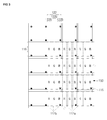
- FIG. 3 is an enlarged plan view of a panel of the liquid crystal display of FIG. 1 .
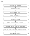
- FIG. 4 is a flowchart illustrating a method of manufacturing the liquid crystal display of FIG. 2b according to an exemplary embodiment of the present invention.
- FIGS. 5a, 5b, 5c, 5d , 5e, 5f , 5g , 5h and 5i are cross-sectional views of the liquid crystal display of FIG. 2b as manufactured in accordance with the sequence depicted in FIG. 4 .
- the X electrode driver 200 applies an electric field to a pixel 150 of the panel 100 through the first transparent electrodes X[1], X[2],... X[n] that are electrically coupled to the panel 100.
- the X electrode driver 200 may supply a voltage to the first transparent electrodes X[1], X[2],... X[n], and the Y electrode driver 300 may supply a voltage to the second transparent electrodes Y[1], Y[2],... Y[m].
- FIGS. 2a and 2b are a perspective view of the panel 100 of the liquid crystal display 1000 of FIG. 1 and a cross-sectional view of the liquid crystal display 1000 of FIG. 1 taken along a line 2b-2b, respectively, according to an exemplary embodiment of the present invention.
- the panel 100 includes a first substrate unit 110, a second substrate unit 120, and liquid crystal 130.
- the first substrate 111 is usually a glass substrate and may be formed of soda lime glass, of neutral borosilicate glass, of non-alkali glass, or an equivalent thereof according to the chemical composition of the glass.
- the present invention is not limited thereto.
- the color filter 112 is formed to cover the upper surface of the first substrate 111. Preferably, the color filter 112 is formed directly on the upper surface of the first substrate 111.
- the color filter 112 includes color photoresists 112b and black matrices 112a disposed between the color photoresists 112b.
- the color photoresists 112b include a red R photoresist, a green G photoresist, and a blue B photoresist, and are arranged in a plurality of lines of rows in the color filter 112. Each color photoresist 112b is spaced apart from its adjacent color photoresist 112b by a black matrix 112a.
- a pixel 150 of the panel 100 includes a R photoresist, a G photoresist, and a B photoresist. That is, one pixel 150 includes three photoresists.
- the black matrices 112a may be formed of resin, of chrome, of carbon black, of titanium oxide, or an equivalent thereof.
- the overcoat layer 113 is formed to cover the upper surface of the color filter 112. Preferably, the overcoat layer 113 is formed directly on the upper surface of the color filter 112. The overcoat layer 113 is provided to make steps between the black matrices 112a and the color photoresisters 112b flat when the color filter 112 is formed.
- the overcoat layer 113 may be formed of acrylic resin, of polyimide resin, or an equivalent thereof. However, the present invention is not limited thereto.
- the insulation film 114 is formed to cover the upper surface of the overcoat layer 113 in order to enhance a contact adhesion between the first transparent electrodes 116 and the overcoat layer 113 above which the first transparent electrodes 116 are formed.
- the insulation film 114 is formed directly on the upper surface of the overcoat layer 113.
- the insulation film 114 may be formed of oxide SiO 2 or an equivalent thereof. However, the present invention is not limited thereto.
- the photo spacers 115 are formed adjacent the pixels 150. However, the present invention is not limited to a number of photo spacers 115 corresponding to the number of pixels 150.
- the photo spacers 115 are formed on or above the black matrices 112a that are generated by the B photoresists that are relatively small, i.e. have a relatively small width in Fig. 2b .
- the present invention is not limited to regions where the photo spacers 115 are formed as shown in Fig. 2b . That is, the photo spacers 115 may be formed in any regions of or above the black matrices 112a as long as the cross-section of the photo spacers 115 does not overlap with the cross sections of the color photoresists 112b.
- the photo spacers 115 may be formed in a selective region using a photolithography process.
- the photo spacers 115 are formed using the photolithography process, thereby preventing degradation of a display quality of the panel 100 due to leakage of light caused by undesired spacers that are formed on the color photoresists 112b.
- the first transparent electrodes 116 are formed to cover the upper surface of the insulation film 114 and are separated from the side surface of the photo spacers 115.
- the first transparent electrodes 116 are arranged in a first direction to cover the color photoresists 112b of the color filter 112.
- the first transparent electrodes 116 may be formed in a row direction. If the first transparent electrodes 116 are formed in the row direction, the second transparent electrodes 122 are formed in the column direction. If the first transparent electrodes 116 are formed in the column direction, the second transparent electrodes 122 are formed in the row direction. That is, the first transparent electrodes 116 and the second transparent electrodes 122 are perpendicular to each other.
- the first transparent electrodes 116 may be formed of indium tin oxide (ITO), of tin oxide (SnO 2 ), or an equivalent thereof. However, the present invention is not limited thereto.
- the second substrate unit 120 includes a second substrate 121 and the second transparent electrodes 122.
- the second substrate 121 may be formed of soda lime glass, of neutral borosilicate glass, of non-alkali glass, or an equivalent thereof according to the chemical composition of the glass.
- the present invention is not limited thereto.
- the second transparent electrodes 122 are arranged between the second substrate 121 and the first transparent electrodes 116.
- the second transparent electrodes 122 are arranged in a second direction to cover the second substrate 121.
- the second transparent electrodes 122 may be formed in a column direction. If the second transparent electrodes 122 are formed in the column direction, the first transparent electrodes 116 are formed in the row direction. If the second transparent electrodes 122 are formed in the row direction, the first transparent electrodes 166 may be formed in the column direction. That is, the first transparent electrodes 116 and the second transparent electrodes 122 are perpendicular to each other.
- the first transparent electrodes 116 and the second transparent electrodes 122 are spaced apart from each other in order to apply an electric field to liquid crystal material therebetween.
- the second transparent electrodes 122 may be formed of indium tin oxide (ITO), of tin oxide (SnO 2 ), or an equivalent thereof.
- ITO indium tin oxide
- SnO 2 tin oxide
- the present invention is not limited thereto.
- the liquid crystal 130 material is provided between the first substrate unit 110 and the second substrate unit 120.
- the liquid crystal material 130 is preferably color super twisted nematic (CSTN) liquid crystal.
- CSTN liquid crystal is suitable for passive-matrix LCD since it uses a transparency that very sharply varies according to an applied voltage having a torsion angle between 240 degrees and 270 degrees.
- FIG. 3 is an enlarged plan view of a panel of the liquid crystal display of FIG. 1 according to an exemplary embodiment of the present invention.
- the panel 100 includes the color photoresists 112b, the photo spacers 115, the first transparent electrodes 116, and the second transparent electrodes 122.
- the color photoresists 112b include an R photoresist, a G photoresist, and a B photoresist, and are arranged in a plurality of lines of rows in the color filter 112.
- the black matrices 112a are disposed between the color photoresists 112b.
- a pixel 150 of the panel 100 includes the R photoresist, the G photoresist, and the B photoresist. That is, one pixel 150 includes three photoresists.
- the photo spacers 115 are formed in some of regions where the black matrices 112a are formed.
- the B photoresists are formed smaller than the R photoresists and the G photoresists.
- the photo spacers 115 are formed in the black matrices 112a that are generated by the B photoresists that are relatively small.
- the present invention is not limited to regions where the photo spacers 115 are formed. That is, the photo spacers 115 can be formed in any regions of the black matrices 112a.
- the photo spacers 115 are formed adjacent the pixels 150, respectively. However, the present invention is not limited to a number of photo spacers 115 corresponding to the number of pixels 150.
- the first transparent electrodes 116 are arranged in a first direction to cover the color photoresists 112b of the color filter 112.
- the first transparent electrodes 116 are arranged in a column direction, they may be formed in a row direction. If the first transparent electrodes 116 are formed in the row direction, the second transparent electrodes 122 are formed in the column direction. If the first transparent electrodes 116 are formed in the column direction, the second transparent electrodes 122 may be formed in the row direction. That is, the first transparent electrodes 116 and the second transparent electrodes 122 are perpendicular to each other. Areas where the first transparent electrodes 116 and the second transparent electrodes 122 cross each other are the pixels 150.
- the second transparent electrodes 122 are arranged in a second direction perpendicular to the first direction that the first transparent electrodes 116 are arranged.
- the second transparent electrodes 122 include second R transparent electrodes 122R that are arranged in the second direction to cover the upper surface of the R photoresists, second G transparent electrodes 122G that are arranged in the second direction to cover the upper surface of the G photoresists, and second B transparent electrodes 122B that are arranged in the second direction to cover the upper surface of the B photoresists.
- the second direction is a row direction
- the second transparent electrodes 122 may be formed in a column direction.
- FIG. 4 is a flowchart illustrating a method of manufacturing the liquid crystal display of FIG. 2B according to an exemplary embodiment of the present invention.
- the method includes the sequence of operations of: preparing a first substrate (S1), forming a color filter (S2), forming an overcoat layer (S3), forming an insulation film (S4), forming photo spacers (S5), forming first transparent electrodes (S6), patterning the first transparent electrodes (S7), combining a second substrate to the first substrate (S8), and injecting liquid crystal (S9).
- FIGS. 5a through 5i are cross-sectional views are cross-sectional views of the liquid crystal display of FIG. 2b as manufactured in accordance with the sequence depicted in FIG. 4 .
- the first substrate 111 in the operation of preparing a first substrate (S1), the first substrate 111, having a first surface 111 a that is approximately or wholly flat and a second surface 111 b that is an opposite to the first surface 111 a and is approximately or wholly flat, is prepared.
- the first substrate 111 may be formed of soda lime glass, of neutral borosilicate glass, of non-alkali glass, or an equivalent thereof according to the chemical composition of the glass.
- the present invention is not limited thereto.
- the black matrices 112a are formed by depositing a light blocking material on, preferably directly on, the first surface 111 a of the first substrate 111, patterning the first substrate 111 using an exposure and developing process, and hardening the first substrate 111.
- the light blocking material may be formed of resin, of chrome, of carbon black, of titanium oxide, or an equivalent thereof.
- the present invention is not limited thereto.
- the color photoresists 112b are formed by sequentially coating light reducing films including pigments expressing colors on the pixels 150 where the black matrices 112a are not formed, performing the exposure and developing process, and hardening the pixels 150, and then the color filter 112 is formed.
- the color photoresists 112b include the R photoresist, the G photoresist, and the B photoresist.
- the overcoat layer 113 is deposited on, preferably directly on, the color filter 112 to cover the color filter 112.
- the overcoat layer 113 flattens steps between the black matrices 112a and the color photoresists 112b when the color filter 112 is formed.
- the overcoat layer 113 may be formed of acrylic resin, or polyimide resin, or an equivalent thereof. However, the present invention is not limited thereto.
- the insulation film 114 is deposited on, preferably directly on, the overcoat layer 113 to cover the overcoat layer 113.
- the insulation film 114 may be formed using any one of selected from a thermal oxidation method, a chemical vapor deposition (CVD) method, an electrochemical oxidation method, or an equivalent thereof. However, the present invention is not limited thereto.
- the insulation film 114 may be formed of oxide SiO 2 or an equivalent thereof. However, the present invention is not limited thereto.
- the photo spacers 115 are formed at desired locations by photo spacer coating on, preferably directly on, the insulation film 114 to cover the insulation film 114 and performing exposure, developing, and etching processes.
- the photo spacers 115 are formed using photolithography, thereby preventing degradation of a display quality of the panel 100 due to leakage of light caused by undesired spacers formed on the color photoresists 112b.
- the photo spacers 115 are formed on or above regions of the black matrices 112a, i.e. entirely on the black matrices 112a such that the photo spacer 115 have no overlap with the color photoresists 112b.
- the first transparent electrodes 116 that are electrotype materials are formed on, preferably directly on, the insulation film 114 and the photo spacer 115 to cover the insulation film 114 and the photo spacers 115.
- the electrotype materials may be formed of indium tin oxide (ITO), of tin oxide (SnO 2 ), or an equivalent thereof.
- ITO indium tin oxide
- SnO 2 tin oxide
- the first transparent electrodes 116 may be formed using a screen printing method, an offset printing method, a photolithography method, or an equivalent method. However, the present invention is not limited thereto.
- the first transparent electrodes 116 are formed in a first direction by patterning the electrotype materials.
- the first transparent electrodes 116 formed on the upper surface and the side surface of the photo spacers 115 are removed. That is, the first transparent electrodes 116 are removed from the photo spacers 115 side surface such that the side surfaces of the first transparent electrodes 116 are spaced apart from the side surfaces of the photo spacers 115.
- the first transparent electrodes 116 are patterned using a photolithography process including photoresist coating, etching of the first transparent electrodes 116 by exposure and developing, and patterning.
- the present invention is not limited thereto.
- the second substrate unit 120 is closely combined to the first substrate unit 110 so that the first transparent electrodes 116 and the color filter 112 cross the second transparent electrodes 122 of the second substrate unit 120.
- a seal (not shown) is printed to make a frame receiving liquid crystal by adhering and fixing the first and second substrate units 110, 120.
- the first and second substrate units 110, 120 are combined using a vacuum method, a high temperature method, and a pressure method.
- the second substrate of the second substrate unit 120 may be formed of soda lime glass, of neutral borosilicate glass, of non-alkali glass, or an equivalent thereof according to the chemical composition of the glass.
- the present invention is not limited thereto.
- the second transparent electrodes 122 of the second substrate unit 120 can be formed and patterned using the same process as used to form and pattern the first transparent electrodes 116.
- the liquid crystal 130 is injected between the first substrate unit 110 and the second substrate unit 120.
- the liquid crystal 130 is filled within an empty space between the first substrate unit 110 and the second substrate unit 120.
- the liquid crystal 130 can be injected into an injection hole between the first substrate unit 110 and the second substrate 120 using a liquid crystal dispenser and then the injection hole is sealed.
- the present invention is not limited thereto.
- the method of manufacturing the liquid crystal display forms the first transparent electrodes 116 as a final process as compared to a conventional method of forming spacers after forming the first transparent electrodes 116, thereby reducing costs incurred in changing a process line for manufacturing a panel of the liquid crystal display and more stably manufacturing the panel than the conventional method.
- the photo spacers 115 are formed before the first transparent electrodes 115 are formed, i.e. the first transparent electrodes 115 are formed after the photo spacers 115, thereby forming the photo spacers 115 using a photolithography process in the same process line as the process line of forming the first substrate unit 110 before the photo spacers 115 are formed.
- the liquid crystal display and the manufacturing method thereof according to the present invention form a spacer in black matrix regions using a photolithography process, so that the spacer are not formed in color photoresist regions, thereby preventing degradation of a display quality due to leakage of light.
- the liquid crystal display and the manufacturing method thereof according to the present invention form transparent electrodes at a final process of manufacturing a panel, thereby reducing costs incurred in a change of a processing line and stably manufacturing the panel.
Landscapes
- Physics & Mathematics (AREA)
- Nonlinear Science (AREA)
- Mathematical Physics (AREA)
- Chemical & Material Sciences (AREA)
- Crystallography & Structural Chemistry (AREA)
- General Physics & Mathematics (AREA)
- Optics & Photonics (AREA)
- Geometry (AREA)
- Liquid Crystal (AREA)
- Optical Filters (AREA)
Abstract
A liquid crystal display includes a first substrate. A color filter covers the first substrate and includes black matrices and color photoresists. Photo spacers upwardly protrude from the black matrices. The photo spacers are formed using a photolithography process so that the spacers are not formed in color photoresist regions. First transparent electrodes cover the color filter on regions other than regions where the photo spacers are formed aned extend in a first direction. A second substrate faces the first substrate. Second transparent electrodes cover the second substrate, are between the second substrate and the first transparent electrodes and extend in a second direction crossing the first direction.
Description
- The present invention relates to a liquid crystal display and a manufacturing method thereof, and more particularly to, a liquid crystal display having a structure that prevents degradation of a display quality due to leakage of light.
- A liquid crystal display (LCD), which is a kind of flat panel display, applies a varying electric voltage to a layer of liquid crystal that has optical properties between those of a conventional liquid and those of a solid crystal, thereby inducing changes in its optical properties. The LCD has wide applications since it has lower power consumption than a conventional cathode ray tube (CRT), is of small volume, may be large-sized and have a fine pitch.
- LCDs are divided into active-matrix LCDs, which use switching devices and twisted nematic (TN) liquid, and passive-matrix LCDs, which use super-twisted nematic (STN) liquid.
- The active-matrix LCD uses a thin film transistor (TFT) as a switch. Whereas, the passive-matrix LCD does not need the TFT, and, as such, requires no complex circuitry.
- The passive-matrix LCD typically uses ball spacers after forming transparent electrodes. The ball spacers are fabricated by scattering spacers mixed with a solvent to a glass substrate on which the transparent electrodes are formed. Spacers are scattered on an upper portion of color photoresist regions, which degrades the display quality of panels due to leakage of light.
- Further, the transparent electrodes are formed using a different processing line from those used to manufacture panels. Therefore, conventional LCDs must change processing lines before and after forming the transparent electrodes in order to manufacture the panels, which degrades the display quality of the panels due to unstable substrates caused by a change in processing lines.
- In accordance with the present invention a liquid crystal display, and a manufacturing method thereof, is provided that forms spacers in a black matrix region using a photolithography process, so that the spacers are not formed in color photoresist regions, thereby preventing degradation of a display quality due to leakage of light.
- Also in accordance with the present invention a liquid crystal display, and a manufacturing method thereof, is provided that forms transparent electrodes as a final process of manufacturing a panel, thereby reducing costs incurred in changing a processing line and allowing for a stable manufacturing of the panel.
- According to an exemplary embodiment of the present invention, a liquid crystal display includes a first substrate. A color filter is formed to cover the first substrate and includes black matrices and color photoresists. A second substrate faces the first substrate. Photo spacers are arranged entirely on the black matrices and are formed to protrude from the black matrices of the color filter toward the second substrate to form a gap between the first and second substrates. In other words, the photo spacers are formed on the black matrices such that they have no overlap with the color photoresists. First transparent electrodes are arranged in a first direction to cover the color filter on regions other than regions where the photo spacers are formed. Second transparent electrodes are arranged in a second direction that crosses the first direction to cover the second substrate and are between the second substrate and the first transparent electrodes.
- The photo spacers may be formed on the black matrices of the cooler filter adjacent to areas where the first and second transparent electrodes cross each other.
- The first transparent electrodes may be separated from the side surfaces of the photo spacers.
- The liquid crystal display may further include an overcoat layer formed to cover the color filter between the color filter and the photo spacers.
- The liquid crystal display may further include an insulation film formed to cover the overcoat layer between the overcoat layer and the photo spacers.
- The liquid crystal display may further include liquid crystal injected between the first transparent electrodes formed on the first substrate and the second transparent electrodes formed on the second substrate.
- The liquid crystal may be color super twisted nematic (CSTN) liquid crystal.
- The color photoresists may include red photoresists, green photoresists, and blue photoresists, and may be arranged in respective rows or columns on the color filter.
- The pixels may correspond to areas where the first and second transparent electrodes cross each other and include a red photoresist, a green photoresist, and a blue photoresist.
- The first and second transparent electrodes may be perpendicular to each other and are spaced apart from each other.
- According to another exemplary embodiment of the present invention, there is provided a method of manufacturing a liquid crystal display. A first substrate is prepared. A color filter is formed to form black matrices and color photoresists to cover the first substrate. Photo spacers are arranged entirely on the black matrices (112a) and formed to upwardly protrude from the black matrices to form a gap between the first substrate and the second substrate. First transparent electrodes are formed to cover the color filter. The first transparent electrodes are patterned to remove the first transparent electrodes formed on an upper surface and side surfaces of the photo spacers and to arrange the first transparent electrodes in a first direction. A second substrate is combined to the first substrate.
- The patterning step of the first transparent electrodes may include removing the first transparent electrodes from the photo spacers such that side surfaces of the first transparent electrodes are spaced apart from side surfaces of the photo spacers.
- The color photoresists may include rows or columns of red photoresists, green photoresists, and blue photoresists on the color filter. In patterning the first transparent electrodes, the first transparent electrodes may be arranged in the first direction according to pixels that include a red photoresist, a green photoresist, and a blue photoresist.
- The method may further include after forming the color filter, forming an overcoat layer to cover the color filter.
- The method may further include after forming the overcoat layer, forming an insulation layer to cover the overcoat layer.
- The method may further include after combining the second substrate to the first substrate, injecting liquid crystal between the first substrate and the second substrate.
-
FIG. 1 is a block diagram of a liquid crystal display according to an exemplary embodiment of the present invention. -
FIGS. 2a and 2b are a perspective view of a panel of the liquid crystal display ofFIG. 1 and a cross-sectional view of the liquid crystal display ofFIG. 1 taken along aline 2b-2b, respectively. -
FIG. 3 is an enlarged plan view of a panel of the liquid crystal display ofFIG. 1 . -
FIG. 4 is a flowchart illustrating a method of manufacturing the liquid crystal display ofFIG. 2b according to an exemplary embodiment of the present invention. -
FIGS. 5a, 5b, 5c, 5d ,5e, 5f ,5g ,5h and 5i are cross-sectional views of the liquid crystal display ofFIG. 2b as manufactured in accordance with the sequence depicted inFIG. 4 . - Like reference numerals in the drawings denote like elements throughout the specification. It will be understood that when an element is referred to as being "electrically coupled" to another element, the element can be directly electrically coupled to another element or through intervening elements.
- Referring to
FIG. 1 , theliquid crystal display 1000 includes a liquid crystal panel 100 (hereinafter also referred to as a "panel), anX electrode driver 200, and aY electrode driver 300. - The
panel 100 includes a plurality of first transparent electrodes X[1], X[2],... X[n] arranged in rows, a plurality of second transparent electrodes Y[1], Y[2],... Y[m] arranged in columns, and a pixels defined by the plurality of first transparent electrodes X[1], X[2],... X[n] and the plurality of second transparent electrodes Y[1], Y[2],... Y[m]. A pixel 150 (also identified by "P" in the drawings) may be formed in an area where one of the first transparent electrodes X[1], X[2],... X[n] and one of the second transparent electrodes Y[1], Y[2],... Y[m] cross each other. - The
X electrode driver 200 applies an electric field to apixel 150 of thepanel 100 through the first transparent electrodes X[1], X[2],... X[n] that are electrically coupled to thepanel 100. - The
Y electrode driver 300 applies an electric field to apixel 150 of thepanel 100 through the second transparent electrodes Y[1], Y[2],... Y[m] that are electrically coupled to thepanel 100. - As described above, the
X electrode driver 200 may supply a voltage to the first transparent electrodes X[1], X[2],... X[n], and theY electrode driver 300 may supply a voltage to the second transparent electrodes Y[1], Y[2],... Y[m]. -
FIGS. 2a and 2b are a perspective view of thepanel 100 of theliquid crystal display 1000 ofFIG. 1 and a cross-sectional view of theliquid crystal display 1000 ofFIG. 1 taken along aline 2b-2b, respectively, according to an exemplary embodiment of the present invention. - Referring to
FIGS. 2a and 2b , thepanel 100 includes afirst substrate unit 110, asecond substrate unit 120, andliquid crystal 130. - The
first substrate unit 110 includes afirst substrate 111, acolor filter 112, anovercoat layer 113, aninsulation film 114,photo spacers 115, and firsttransparent electrodes 116. - The
first substrate 111 is usually a glass substrate and may be formed of soda lime glass, of neutral borosilicate glass, of non-alkali glass, or an equivalent thereof according to the chemical composition of the glass. However, the present invention is not limited thereto. - The
color filter 112 is formed to cover the upper surface of thefirst substrate 111. Preferably, thecolor filter 112 is formed directly on the upper surface of thefirst substrate 111. Thecolor filter 112 includescolor photoresists 112b andblack matrices 112a disposed between thecolor photoresists 112b. Thecolor photoresists 112b include a red R photoresist, a green G photoresist, and a blue B photoresist, and are arranged in a plurality of lines of rows in thecolor filter 112. Eachcolor photoresist 112b is spaced apart from itsadjacent color photoresist 112b by ablack matrix 112a. Apixel 150 of thepanel 100 includes a R photoresist, a G photoresist, and a B photoresist. That is, onepixel 150 includes three photoresists. Theblack matrices 112a may be formed of resin, of chrome, of carbon black, of titanium oxide, or an equivalent thereof. - The
overcoat layer 113 is formed to cover the upper surface of thecolor filter 112. Preferably, theovercoat layer 113 is formed directly on the upper surface of thecolor filter 112. Theovercoat layer 113 is provided to make steps between theblack matrices 112a and thecolor photoresisters 112b flat when thecolor filter 112 is formed. Theovercoat layer 113 may be formed of acrylic resin, of polyimide resin, or an equivalent thereof. However, the present invention is not limited thereto. - The
insulation film 114 is formed to cover the upper surface of theovercoat layer 113 in order to enhance a contact adhesion between the firsttransparent electrodes 116 and theovercoat layer 113 above which the firsttransparent electrodes 116 are formed. Preferably, theinsulation film 114 is formed directly on the upper surface of theovercoat layer 113. Theinsulation film 114 may be formed of oxide SiO2 or an equivalent thereof. However, the present invention is not limited thereto. - The photo spacers 115 are on, preferably directly on, the
insulation film 114 and are formed in regions entirely corresponding to regions where theblack matrices 112a of thecolor filter 112 are formed. In other words, thephoto spacers 115 are formed such that they are not formed on or above regions where thecolor photoresits 112b of thecolor filter 112 are formed. In yet other words, thephoto spacers 115 have no overlap with thecolor photoresists 112b. The photo spacers 115 are formed to control a cell gap between thefirst substrate unit 110 and thesecond substrate unit 120 in order to maintain a constant thickness of theliquid crystal 130. The photo spacers 115 have a stronger contact adhesion with thefirst substrate unit 110 than that with thesecond substrate unit 120. The photo spacers 115 are formed adjacent thepixels 150. However, the present invention is not limited to a number ofphoto spacers 115 corresponding to the number ofpixels 150. The photo spacers 115 are formed on or above theblack matrices 112a that are generated by the B photoresists that are relatively small, i.e. have a relatively small width inFig. 2b . However, the present invention is not limited to regions where thephoto spacers 115 are formed as shown inFig. 2b . That is, thephoto spacers 115 may be formed in any regions of or above theblack matrices 112a as long as the cross-section of thephoto spacers 115 does not overlap with the cross sections of thecolor photoresists 112b. The photo spacers 115 may be formed in a selective region using a photolithography process. The photo spacers 115 are formed using the photolithography process, thereby preventing degradation of a display quality of thepanel 100 due to leakage of light caused by undesired spacers that are formed on thecolor photoresists 112b. - The first
transparent electrodes 116 are formed to cover the upper surface of theinsulation film 114 and are separated from the side surface of thephoto spacers 115. The firsttransparent electrodes 116 are arranged in a first direction to cover thecolor photoresists 112b of thecolor filter 112. In the present embodiment, although the firsttransparent electrodes 116 are arranged in a column direction, they may be formed in a row direction. If the firsttransparent electrodes 116 are formed in the row direction, the secondtransparent electrodes 122 are formed in the column direction. If the firsttransparent electrodes 116 are formed in the column direction, the secondtransparent electrodes 122 are formed in the row direction. That is, the firsttransparent electrodes 116 and the secondtransparent electrodes 122 are perpendicular to each other. The firsttransparent electrodes 116 may be formed of indium tin oxide (ITO), of tin oxide (SnO2), or an equivalent thereof. However, the present invention is not limited thereto. - The
second substrate unit 120 includes asecond substrate 121 and the secondtransparent electrodes 122. - The
second substrate 121 may be formed of soda lime glass, of neutral borosilicate glass, of non-alkali glass, or an equivalent thereof according to the chemical composition of the glass. However, the present invention is not limited thereto. - The second
transparent electrodes 122 are arranged between thesecond substrate 121 and the firsttransparent electrodes 116. The secondtransparent electrodes 122 are arranged in a second direction to cover thesecond substrate 121. In the present embodiment, although the secondtransparent electrodes 122 are arranged in a row direction, they may be formed in a column direction. If the secondtransparent electrodes 122 are formed in the column direction, the firsttransparent electrodes 116 are formed in the row direction. If the secondtransparent electrodes 122 are formed in the row direction, the first transparent electrodes 166 may be formed in the column direction. That is, the firsttransparent electrodes 116 and the secondtransparent electrodes 122 are perpendicular to each other. The firsttransparent electrodes 116 and the secondtransparent electrodes 122 are spaced apart from each other in order to apply an electric field to liquid crystal material therebetween. The secondtransparent electrodes 122 may be formed of indium tin oxide (ITO), of tin oxide (SnO2), or an equivalent thereof. However, the present invention is not limited thereto. - The
liquid crystal 130 material is provided between thefirst substrate unit 110 and thesecond substrate unit 120. An electric field applied between the firsttransparent electrodes 116 and the secondtransparent electrodes 122, changes an arrangement of liquid crystal molecules. Theliquid crystal material 130 is preferably color super twisted nematic (CSTN) liquid crystal. The CSTN liquid crystal is suitable for passive-matrix LCD since it uses a transparency that very sharply varies according to an applied voltage having a torsion angle between 240 degrees and 270 degrees. -
FIG. 3 is an enlarged plan view of a panel of the liquid crystal display ofFIG. 1 according to an exemplary embodiment of the present invention. Referring toFIG. 3 , thepanel 100 includes thecolor photoresists 112b, thephoto spacers 115, the firsttransparent electrodes 116, and the secondtransparent electrodes 122. - The
color photoresists 112b include an R photoresist, a G photoresist, and a B photoresist, and are arranged in a plurality of lines of rows in thecolor filter 112. Theblack matrices 112a are disposed between thecolor photoresists 112b. Apixel 150 of thepanel 100 includes the R photoresist, the G photoresist, and the B photoresist. That is, onepixel 150 includes three photoresists. - The photo spacers 115 are formed in some of regions where the
black matrices 112a are formed. The B photoresists are formed smaller than the R photoresists and the G photoresists. The photo spacers 115 are formed in theblack matrices 112a that are generated by the B photoresists that are relatively small. However, the present invention is not limited to regions where thephoto spacers 115 are formed. That is, thephoto spacers 115 can be formed in any regions of theblack matrices 112a. The photo spacers 115 are formed adjacent thepixels 150, respectively. However, the present invention is not limited to a number ofphoto spacers 115 corresponding to the number ofpixels 150. - The first
transparent electrodes 116 are arranged in a first direction to cover thecolor photoresists 112b of thecolor filter 112. In the present exemplary embodiment, although the firsttransparent electrodes 116 are arranged in a column direction, they may be formed in a row direction. If the firsttransparent electrodes 116 are formed in the row direction, the secondtransparent electrodes 122 are formed in the column direction. If the firsttransparent electrodes 116 are formed in the column direction, the secondtransparent electrodes 122 may be formed in the row direction. That is, the firsttransparent electrodes 116 and the secondtransparent electrodes 122 are perpendicular to each other. Areas where the firsttransparent electrodes 116 and the secondtransparent electrodes 122 cross each other are thepixels 150. - The second
transparent electrodes 122 are arranged in a second direction perpendicular to the first direction that the firsttransparent electrodes 116 are arranged. The secondtransparent electrodes 122 include second Rtransparent electrodes 122R that are arranged in the second direction to cover the upper surface of the R photoresists, second G transparent electrodes 122G that are arranged in the second direction to cover the upper surface of the G photoresists, and second Btransparent electrodes 122B that are arranged in the second direction to cover the upper surface of the B photoresists. In the present exemplary embodiment, although the second direction is a row direction, the secondtransparent electrodes 122 may be formed in a column direction. If the second direction is the column direction, the firsttransparent electrodes 116 that are arranged in the first direction are formed in the column direction. Points where the firsttransparent electrodes 116 and the secondtransparent electrodes 122 cross each other are thepixels 150. If an electric field is applied between the firsttransparent electrodes 116 and the secondtransparent electrodes pixels 150 of thepanel 100 display an image according to the arrangement of liquid crystal molecules. - A method of manufacturing a liquid crystal display as described above will now be described.
-
FIG. 4 is a flowchart illustrating a method of manufacturing the liquid crystal display ofFIG. 2B according to an exemplary embodiment of the present invention. Referring toFIG. 4 , the method includes the sequence of operations of: preparing a first substrate (S1), forming a color filter (S2), forming an overcoat layer (S3), forming an insulation film (S4), forming photo spacers (S5), forming first transparent electrodes (S6), patterning the first transparent electrodes (S7), combining a second substrate to the first substrate (S8), and injecting liquid crystal (S9). -
FIGS. 5a through 5i are cross-sectional views are cross-sectional views of the liquid crystal display ofFIG. 2b as manufactured in accordance with the sequence depicted inFIG. 4 . - Referring to
FIG. 5a , in the operation of preparing a first substrate (S1), thefirst substrate 111, having afirst surface 111 a that is approximately or wholly flat and asecond surface 111 b that is an opposite to thefirst surface 111 a and is approximately or wholly flat, is prepared. Thefirst substrate 111 may be formed of soda lime glass, of neutral borosilicate glass, of non-alkali glass, or an equivalent thereof according to the chemical composition of the glass. However, the present invention is not limited thereto. - Referring to
FIG. 5b , in the operation of forming a color filter (S2), theblack matrices 112a are formed by depositing a light blocking material on, preferably directly on, thefirst surface 111 a of thefirst substrate 111, patterning thefirst substrate 111 using an exposure and developing process, and hardening thefirst substrate 111. The light blocking material may be formed of resin, of chrome, of carbon black, of titanium oxide, or an equivalent thereof. However, the present invention is not limited thereto. Thecolor photoresists 112b are formed by sequentially coating light reducing films including pigments expressing colors on thepixels 150 where theblack matrices 112a are not formed, performing the exposure and developing process, and hardening thepixels 150, and then thecolor filter 112 is formed. Thecolor photoresists 112b include the R photoresist, the G photoresist, and the B photoresist. - Referring to
FIG. 5c , in the operation of forming an overcoat layer (S3), theovercoat layer 113 is deposited on, preferably directly on, thecolor filter 112 to cover thecolor filter 112. Theovercoat layer 113 flattens steps between theblack matrices 112a and thecolor photoresists 112b when thecolor filter 112 is formed. Theovercoat layer 113 may be formed of acrylic resin, or polyimide resin, or an equivalent thereof. However, the present invention is not limited thereto. - Referring to
FIG. 5d , in the operation of forming an insulation film (S4), theinsulation film 114 is deposited on, preferably directly on, theovercoat layer 113 to cover theovercoat layer 113. Theinsulation film 114 may be formed using any one of selected from a thermal oxidation method, a chemical vapor deposition (CVD) method, an electrochemical oxidation method, or an equivalent thereof. However, the present invention is not limited thereto. Theinsulation film 114 may be formed of oxide SiO2 or an equivalent thereof. However, the present invention is not limited thereto. - Referring to
FIG. 5e , in the operation of forming photo spacers (S5), thephoto spacers 115 are formed at desired locations by photo spacer coating on, preferably directly on, theinsulation film 114 to cover theinsulation film 114 and performing exposure, developing, and etching processes. The photo spacers 115 are formed using photolithography, thereby preventing degradation of a display quality of thepanel 100 due to leakage of light caused by undesired spacers formed on thecolor photoresists 112b. The photo spacers 115 are formed on or above regions of theblack matrices 112a, i.e. entirely on theblack matrices 112a such that thephoto spacer 115 have no overlap with thecolor photoresists 112b. - Referring to
FIG. 5f , in the operation of forming first transparent electrodes (S6), the firsttransparent electrodes 116 that are electrotype materials are formed on, preferably directly on, theinsulation film 114 and thephoto spacer 115 to cover theinsulation film 114 and thephoto spacers 115. The electrotype materials may be formed of indium tin oxide (ITO), of tin oxide (SnO2), or an equivalent thereof. However, the present invention is not limited thereto. The firsttransparent electrodes 116 may be formed using a screen printing method, an offset printing method, a photolithography method, or an equivalent method. However, the present invention is not limited thereto. - Referring to
FIG. 5g , in the operation of patterning the first transparent electrodes 116 (S7), the firsttransparent electrodes 116 are formed in a first direction by patterning the electrotype materials. When patterning the electrotype materials, the firsttransparent electrodes 116 formed on the upper surface and the side surface of thephoto spacers 115 are removed. That is, the firsttransparent electrodes 116 are removed from thephoto spacers 115 side surface such that the side surfaces of the firsttransparent electrodes 116 are spaced apart from the side surfaces of thephoto spacers 115. The firsttransparent electrodes 116 are patterned using a photolithography process including photoresist coating, etching of the firsttransparent electrodes 116 by exposure and developing, and patterning. However, the present invention is not limited thereto. - Referring to
FIG. 5h , in the operation of combining a second substrate to a first substrate (S8), thesecond substrate unit 120 is closely combined to thefirst substrate unit 110 so that the firsttransparent electrodes 116 and thecolor filter 112 cross the secondtransparent electrodes 122 of thesecond substrate unit 120. A seal (not shown) is printed to make a frame receiving liquid crystal by adhering and fixing the first andsecond substrate units second substrate units second substrate unit 120 may be formed of soda lime glass, of neutral borosilicate glass, of non-alkali glass, or an equivalent thereof according to the chemical composition of the glass. However, the present invention is not limited thereto. The secondtransparent electrodes 122 of thesecond substrate unit 120 can be formed and patterned using the same process as used to form and pattern the firsttransparent electrodes 116. - Referring to
FIG. 5i , in the operation of injecting liquid crystal (S9), theliquid crystal 130 is injected between thefirst substrate unit 110 and thesecond substrate unit 120. Theliquid crystal 130 is filled within an empty space between thefirst substrate unit 110 and thesecond substrate unit 120. Theliquid crystal 130 can be injected into an injection hole between thefirst substrate unit 110 and thesecond substrate 120 using a liquid crystal dispenser and then the injection hole is sealed. However, the present invention is not limited thereto. - The method of manufacturing the liquid crystal display forms the first
transparent electrodes 116 as a final process as compared to a conventional method of forming spacers after forming the firsttransparent electrodes 116, thereby reducing costs incurred in changing a process line for manufacturing a panel of the liquid crystal display and more stably manufacturing the panel than the conventional method. According to the present invention, thephoto spacers 115 are formed before the firsttransparent electrodes 115 are formed, i.e. the firsttransparent electrodes 115 are formed after thephoto spacers 115, thereby forming thephoto spacers 115 using a photolithography process in the same process line as the process line of forming thefirst substrate unit 110 before thephoto spacers 115 are formed. - The liquid crystal display and the manufacturing method thereof according to the present invention form a spacer in black matrix regions using a photolithography process, so that the spacer are not formed in color photoresist regions, thereby preventing degradation of a display quality due to leakage of light.
- The liquid crystal display and the manufacturing method thereof according to the present invention form transparent electrodes at a final process of manufacturing a panel, thereby reducing costs incurred in a change of a processing line and stably manufacturing the panel.
- While the present invention has been particularly shown and described with reference to exemplary embodiments thereof, it will be understood by those skilled in the art that various changes in form and details may be made therein without departing from the scope of the invention as defined by the appended claims. The exemplary embodiments should be considered in a descriptive sense only and not for purposes of limitation. Therefore, the scope of the present invention is defined not by the detailed description of the invention but by the appended claims, and all differences within the scope of the present invention will be construed as being included in the present invention.
Claims (14)
- A liquid crystal display, comprising:a first substrate (111);a color filter (112) covering the first substrate (111) and including black matrices (112a) and color photoresists (112b);a second substrate (121) facing the first substrate (111);photo spacers (115) arranged entirely on the black matrices (112a) and protruding from the black matrices (112a) toward the second substrate (121) to form a gap between the first substrate (111) and the second substrate (121);first transparent electrodes (116), covering the color filter (112) on regions other than regions where the photo spacers (115) are formed, and extending in a first direction; andsecond transparent electrodes (122) covering the second substrate (121) between the second substrate (121) and the first transparent electrodes (116) and extending in a second direction crossing the first direction.
- The liquid crystal display of claim 1, wherein the photo spacers (115) are arranged on the black matrices (112a) adjacent to areas where the first transparent electrodes (116) and the second transparent electrodes (122) cross each other.
- The liquid crystal display of claim 1 or 2, wherein the first transparent electrodes (116) are arranged to be spaced apart from side surfaces of the photo spacers (115).
- The liquid crystal display of one of the previous claims, further comprising an overcoat layer (113) covering the color filter (112) between the color filter (112) and the photo spacers (115).
- The liquid crystal display of claim 4, further comprising an insulation film (114) covering the overcoat layer (113) between the overcoat layer (113) and the photo spacers (115).
- The liquid crystal display of one of the previous claims, further comprising liquid crystal material (130) provided between the first transparent electrodes (116) and the second transparent electrodes (122).
- The liquid crystal display of claim 6, wherein the liquid crystal material (130) is color super twisted nematic liquid crystal.
- The liquid crystal display of one of the previous claims, wherein the color photoresists (112b) include red photoresists, green photoresists, and blue photoresists, and are in respective rows and columns on the color filter (112).
- The liquid crystal display of claim 8, wherein pixels (150) correspond to areas where the first transparent electrodes (116) and the second transparent electrodes (122) cross each other and include ones of the red photoresists, the green photoresists, and the blue photoresists.
- The liquid crystal display of one of the previous claims, wherein the first transparent electrodes (116) and the second transparent electrodes (122) are perpendicular to and spaced apart from each other.
- A method of manufacturing a liquid crystal display, comprising:preparing a first substrate (111);forming a color filter (112) having black matrices (112a) and color photoresists (112b) covering the first substrate (111);forming photo spacers (115) entirely on the black matrices (112a) and upwardly protruding from the black matrices (112a) to form a gap between the first substrate (111) and the second substrate (121);forming first transparent electrodes (116) covering the color filter (112) and the photo spacers (115);patterning the first transparent electrodes (116) to remove the first transparent electrodes (116) formed on an upper surface and side surfaces of the photo spacers (115) and to arrange the first transparent electrodes (116) in a first direction; andcombining a second substrate (121) to the first substrate (111).
- The method of claim 11, further comprising, after forming the color filter (112), forming an overcoat layer (113) covering the color filter (112).
- The method of claim 12, further comprising, after forming the overcoat layer (113), forming an insulation layer (114) covering the overcoat layer (113).
- The method of one of the previous claims 11 to 13, further comprising, after combining the second substrate (121) to the first substrate (111), injecting liquid crystal material between the first substrate and the second substrate (121).
Applications Claiming Priority (1)
| Application Number | Priority Date | Filing Date | Title |
|---|---|---|---|
| KR1020080008689A KR100933867B1 (en) | 2008-01-28 | 2008-01-28 | Liquid crystal display device and manufacturing method thereof |
Publications (1)
| Publication Number | Publication Date |
|---|---|
| EP2083317A1 true EP2083317A1 (en) | 2009-07-29 |
Family
ID=40561733
Family Applications (1)
| Application Number | Title | Priority Date | Filing Date |
|---|---|---|---|
| EP09151321A Withdrawn EP2083317A1 (en) | 2008-01-28 | 2009-01-26 | Liquid crystal display and manufacturing method thereof |
Country Status (5)
| Country | Link |
|---|---|
| US (1) | US20090190075A1 (en) |
| EP (1) | EP2083317A1 (en) |
| JP (1) | JP2009175732A (en) |
| KR (1) | KR100933867B1 (en) |
| CN (1) | CN101498855A (en) |
Families Citing this family (3)
| Publication number | Priority date | Publication date | Assignee | Title |
|---|---|---|---|---|
| CN101458417B (en) * | 2008-12-17 | 2012-10-10 | 康佳集团股份有限公司 | Display panel |
| JP5733065B2 (en) * | 2011-07-07 | 2015-06-10 | 三菱電機株式会社 | Liquid crystal display panel and repair method |
| US12282219B2 (en) * | 2021-09-15 | 2025-04-22 | Beijing Boe Display Technology Co., Ltd. | Liquid crystal display panel and method of manufacturing the same, and display apparatus |
Citations (3)
| Publication number | Priority date | Publication date | Assignee | Title |
|---|---|---|---|---|
| EP0992841A1 (en) * | 1997-06-13 | 2000-04-12 | Sekisui Chemical Co., Ltd. | Liquid crystal display and method of manufacturing the same |
| JP2001159755A (en) * | 1999-05-10 | 2001-06-12 | Citizen Watch Co Ltd | Liquid crystal display device and method of producing the same |
| US20050110922A1 (en) * | 2003-11-24 | 2005-05-26 | Dong-Hoon Lee | Color filter panel and its fabrication method using back exposure |
Family Cites Families (13)
| Publication number | Priority date | Publication date | Assignee | Title |
|---|---|---|---|---|
| US110922A (en) * | 1871-01-10 | Improvement in street-lamps | ||
| US4448491A (en) * | 1979-08-08 | 1984-05-15 | Canon Kabushiki Kaisha | Image display apparatus |
| JPH05257014A (en) * | 1990-11-21 | 1993-10-08 | Fuji Photo Film Co Ltd | Phase difference film and liquid crystal display device using the same |
| JP3999824B2 (en) * | 1995-08-21 | 2007-10-31 | 東芝電子エンジニアリング株式会社 | Liquid crystal display element |
| JP2001183513A (en) * | 1999-12-22 | 2001-07-06 | Hitachi Ltd | Color filter and manufacturing method thereof, color liquid crystal display device |
| JP2001183648A (en) * | 1999-12-24 | 2001-07-06 | Nec Corp | Color liquid crystal display device and method of producing the same |
| JP2001296530A (en) * | 2000-04-12 | 2001-10-26 | Seiko Epson Corp | Electro-optical device and method of manufacturing the same |
| JP3824889B2 (en) * | 2000-07-14 | 2006-09-20 | セイコーエプソン株式会社 | Color filter substrate, liquid crystal device, and manufacturing method thereof |
| KR20020056711A (en) * | 2000-12-29 | 2002-07-10 | 주식회사 현대 디스플레이 테크놀로지 | Method for manufacturing lcd |
| JP4048085B2 (en) | 2002-07-24 | 2008-02-13 | 住友化学株式会社 | Color filter for liquid crystal and manufacturing method thereof |
| JP2005134543A (en) * | 2003-10-29 | 2005-05-26 | Seiko Epson Corp | A method for inspecting a substrate for an electro-optical device and a method for manufacturing a substrate for an electro-optical device. |
| JP2006267782A (en) * | 2005-03-25 | 2006-10-05 | Sanyo Epson Imaging Devices Corp | Electrooptical apparatus and electronic equipment |
| JP2007206352A (en) | 2006-02-01 | 2007-08-16 | Kyodo Printing Co Ltd | Manufacturing method of element substrate for liquid crystal display device, liquid crystal display device and manufacturing method thereof |
-
2008
- 2008-01-28 KR KR1020080008689A patent/KR100933867B1/en not_active Expired - Fee Related
- 2008-12-22 US US12/341,816 patent/US20090190075A1/en not_active Abandoned
-
2009
- 2009-01-09 JP JP2009003848A patent/JP2009175732A/en active Pending
- 2009-01-23 CN CNA2009100009772A patent/CN101498855A/en active Pending
- 2009-01-26 EP EP09151321A patent/EP2083317A1/en not_active Withdrawn
Patent Citations (3)
| Publication number | Priority date | Publication date | Assignee | Title |
|---|---|---|---|---|
| EP0992841A1 (en) * | 1997-06-13 | 2000-04-12 | Sekisui Chemical Co., Ltd. | Liquid crystal display and method of manufacturing the same |
| JP2001159755A (en) * | 1999-05-10 | 2001-06-12 | Citizen Watch Co Ltd | Liquid crystal display device and method of producing the same |
| US20050110922A1 (en) * | 2003-11-24 | 2005-05-26 | Dong-Hoon Lee | Color filter panel and its fabrication method using back exposure |
Also Published As
| Publication number | Publication date |
|---|---|
| US20090190075A1 (en) | 2009-07-30 |
| KR20090082753A (en) | 2009-07-31 |
| CN101498855A (en) | 2009-08-05 |
| KR100933867B1 (en) | 2009-12-24 |
| JP2009175732A (en) | 2009-08-06 |
Similar Documents
| Publication | Publication Date | Title |
|---|---|---|
| US7656496B2 (en) | Liquid crystal display device and method for fabricating the same | |
| US7502090B2 (en) | Liquid crystal display device and method of fabricating the same | |
| US7852450B2 (en) | Liquid crystal display device and method of fabricating the same | |
| US20090258451A1 (en) | Liquid crystal display device | |
| US7821612B2 (en) | Color filter array panel and liquid crystal display including the same | |
| KR100640216B1 (en) | Liquid crystal display panel and manufacturing method thereof | |
| JP2010039187A (en) | Display element | |
| US7248312B2 (en) | Liquid crystal display panel and fabricating method thereof | |
| US8514360B2 (en) | LCD device | |
| US5847793A (en) | Liquid crystal display apparatus and fabrication process thereof | |
| EP2083317A1 (en) | Liquid crystal display and manufacturing method thereof | |
| KR20050114123A (en) | Liquid crystal display panel and method for fabricating the same | |
| KR100603669B1 (en) | LCD and its manufacturing method | |
| KR20100049383A (en) | In-plane switching liquid crystal display device | |
| JP2002148624A (en) | Liquid crystal display device, color filter, and method for producing them | |
| KR20040012309A (en) | liquid crystal panel including patterned spacer | |
| KR100780831B1 (en) | Display device | |
| KR20070077998A (en) | Color filter substrate, manufacturing method thereof and liquid crystal display panel including the same | |
| KR20130066917A (en) | Fringe field switching liquid crystal display device having align key and method of fabricating fringe field switching liquid crystal display device using thereof | |
| KR100928483B1 (en) | Manufacturing method of multi-domain liquid crystal display | |
| KR100628273B1 (en) | Transverse electric field type liquid crystal display device and manufacturing method thereof | |
| KR20060031336A (en) | Liquid Crystal Display Device with Patterned Spacer | |
| KR100959777B1 (en) | Manufacturing method of liquid crystal display panel | |
| JP2010096809A (en) | Liquid crystal display and method for manufacturing the same | |
| KR20060093971A (en) | LCD panel and manufacturing method |
Legal Events
| Date | Code | Title | Description |
|---|---|---|---|
| PUAI | Public reference made under article 153(3) epc to a published international application that has entered the european phase |
Free format text: ORIGINAL CODE: 0009012 |
|
| 17P | Request for examination filed |
Effective date: 20090126 |
|
| AK | Designated contracting states |
Kind code of ref document: A1 Designated state(s): AT BE BG CH CY CZ DE DK EE ES FI FR GB GR HR HU IE IS IT LI LT LU LV MC MK MT NL NO PL PT RO SE SI SK TR |
|
| AX | Request for extension of the european patent |
Extension state: AL BA RS |
|
| AKX | Designation fees paid |
Designated state(s): DE FR GB |
|
| STAA | Information on the status of an ep patent application or granted ep patent |
Free format text: STATUS: THE APPLICATION IS DEEMED TO BE WITHDRAWN |
|
| 18D | Application deemed to be withdrawn |
Effective date: 20120801 |