EP2083317A1 - Flüssigkristallanzeige und Herstellungsverfahren dafür - Google Patents
Flüssigkristallanzeige und Herstellungsverfahren dafür Download PDFInfo
- Publication number
- EP2083317A1 EP2083317A1 EP09151321A EP09151321A EP2083317A1 EP 2083317 A1 EP2083317 A1 EP 2083317A1 EP 09151321 A EP09151321 A EP 09151321A EP 09151321 A EP09151321 A EP 09151321A EP 2083317 A1 EP2083317 A1 EP 2083317A1
- Authority
- EP
- European Patent Office
- Prior art keywords
- transparent electrodes
- substrate
- liquid crystal
- crystal display
- photoresists
- Prior art date
- Legal status (The legal status is an assumption and is not a legal conclusion. Google has not performed a legal analysis and makes no representation as to the accuracy of the status listed.)
- Withdrawn
Links
Images


Classifications
-
- G—PHYSICS
- G02—OPTICS
- G02F—OPTICAL DEVICES OR ARRANGEMENTS FOR THE CONTROL OF LIGHT BY MODIFICATION OF THE OPTICAL PROPERTIES OF THE MEDIA OF THE ELEMENTS INVOLVED THEREIN; NON-LINEAR OPTICS; FREQUENCY-CHANGING OF LIGHT; OPTICAL LOGIC ELEMENTS; OPTICAL ANALOGUE/DIGITAL CONVERTERS
- G02F1/00—Devices or arrangements for the control of the intensity, colour, phase, polarisation or direction of light arriving from an independent light source, e.g. switching, gating or modulating; Non-linear optics
- G02F1/01—Devices or arrangements for the control of the intensity, colour, phase, polarisation or direction of light arriving from an independent light source, e.g. switching, gating or modulating; Non-linear optics for the control of the intensity, phase, polarisation or colour
- G02F1/13—Devices or arrangements for the control of the intensity, colour, phase, polarisation or direction of light arriving from an independent light source, e.g. switching, gating or modulating; Non-linear optics for the control of the intensity, phase, polarisation or colour based on liquid crystals, e.g. single liquid crystal display cells
- G02F1/133—Constructional arrangements; Operation of liquid crystal cells; Circuit arrangements
- G02F1/1333—Constructional arrangements; Manufacturing methods
- G02F1/1339—Gaskets; Spacers; Sealing of cells
- G02F1/13394—Gaskets; Spacers; Sealing of cells spacers regularly patterned on the cell subtrate, e.g. walls, pillars
-
- G—PHYSICS
- G02—OPTICS
- G02F—OPTICAL DEVICES OR ARRANGEMENTS FOR THE CONTROL OF LIGHT BY MODIFICATION OF THE OPTICAL PROPERTIES OF THE MEDIA OF THE ELEMENTS INVOLVED THEREIN; NON-LINEAR OPTICS; FREQUENCY-CHANGING OF LIGHT; OPTICAL LOGIC ELEMENTS; OPTICAL ANALOGUE/DIGITAL CONVERTERS
- G02F1/00—Devices or arrangements for the control of the intensity, colour, phase, polarisation or direction of light arriving from an independent light source, e.g. switching, gating or modulating; Non-linear optics
- G02F1/01—Devices or arrangements for the control of the intensity, colour, phase, polarisation or direction of light arriving from an independent light source, e.g. switching, gating or modulating; Non-linear optics for the control of the intensity, phase, polarisation or colour
- G02F1/13—Devices or arrangements for the control of the intensity, colour, phase, polarisation or direction of light arriving from an independent light source, e.g. switching, gating or modulating; Non-linear optics for the control of the intensity, phase, polarisation or colour based on liquid crystals, e.g. single liquid crystal display cells
- G02F1/133—Constructional arrangements; Operation of liquid crystal cells; Circuit arrangements
- G02F1/1333—Constructional arrangements; Manufacturing methods
- G02F1/1339—Gaskets; Spacers; Sealing of cells
-
- G—PHYSICS
- G02—OPTICS
- G02F—OPTICAL DEVICES OR ARRANGEMENTS FOR THE CONTROL OF LIGHT BY MODIFICATION OF THE OPTICAL PROPERTIES OF THE MEDIA OF THE ELEMENTS INVOLVED THEREIN; NON-LINEAR OPTICS; FREQUENCY-CHANGING OF LIGHT; OPTICAL LOGIC ELEMENTS; OPTICAL ANALOGUE/DIGITAL CONVERTERS
- G02F1/00—Devices or arrangements for the control of the intensity, colour, phase, polarisation or direction of light arriving from an independent light source, e.g. switching, gating or modulating; Non-linear optics
- G02F1/01—Devices or arrangements for the control of the intensity, colour, phase, polarisation or direction of light arriving from an independent light source, e.g. switching, gating or modulating; Non-linear optics for the control of the intensity, phase, polarisation or colour
- G02F1/13—Devices or arrangements for the control of the intensity, colour, phase, polarisation or direction of light arriving from an independent light source, e.g. switching, gating or modulating; Non-linear optics for the control of the intensity, phase, polarisation or colour based on liquid crystals, e.g. single liquid crystal display cells
- G02F1/133—Constructional arrangements; Operation of liquid crystal cells; Circuit arrangements
- G02F1/1333—Constructional arrangements; Manufacturing methods
- G02F1/1335—Structural association of cells with optical devices, e.g. polarisers or reflectors
- G02F1/133509—Filters, e.g. light shielding masks
- G02F1/133512—Light shielding layers, e.g. black matrix
-
- G—PHYSICS
- G02—OPTICS
- G02F—OPTICAL DEVICES OR ARRANGEMENTS FOR THE CONTROL OF LIGHT BY MODIFICATION OF THE OPTICAL PROPERTIES OF THE MEDIA OF THE ELEMENTS INVOLVED THEREIN; NON-LINEAR OPTICS; FREQUENCY-CHANGING OF LIGHT; OPTICAL LOGIC ELEMENTS; OPTICAL ANALOGUE/DIGITAL CONVERTERS
- G02F1/00—Devices or arrangements for the control of the intensity, colour, phase, polarisation or direction of light arriving from an independent light source, e.g. switching, gating or modulating; Non-linear optics
- G02F1/01—Devices or arrangements for the control of the intensity, colour, phase, polarisation or direction of light arriving from an independent light source, e.g. switching, gating or modulating; Non-linear optics for the control of the intensity, phase, polarisation or colour
- G02F1/13—Devices or arrangements for the control of the intensity, colour, phase, polarisation or direction of light arriving from an independent light source, e.g. switching, gating or modulating; Non-linear optics for the control of the intensity, phase, polarisation or colour based on liquid crystals, e.g. single liquid crystal display cells
- G02F1/133—Constructional arrangements; Operation of liquid crystal cells; Circuit arrangements
- G02F1/1333—Constructional arrangements; Manufacturing methods
- G02F1/1343—Electrodes
- G02F1/134309—Electrodes characterised by their geometrical arrangement
- G02F1/134336—Matrix
-
- G—PHYSICS
- G02—OPTICS
- G02F—OPTICAL DEVICES OR ARRANGEMENTS FOR THE CONTROL OF LIGHT BY MODIFICATION OF THE OPTICAL PROPERTIES OF THE MEDIA OF THE ELEMENTS INVOLVED THEREIN; NON-LINEAR OPTICS; FREQUENCY-CHANGING OF LIGHT; OPTICAL LOGIC ELEMENTS; OPTICAL ANALOGUE/DIGITAL CONVERTERS
- G02F1/00—Devices or arrangements for the control of the intensity, colour, phase, polarisation or direction of light arriving from an independent light source, e.g. switching, gating or modulating; Non-linear optics
- G02F1/01—Devices or arrangements for the control of the intensity, colour, phase, polarisation or direction of light arriving from an independent light source, e.g. switching, gating or modulating; Non-linear optics for the control of the intensity, phase, polarisation or colour
- G02F1/13—Devices or arrangements for the control of the intensity, colour, phase, polarisation or direction of light arriving from an independent light source, e.g. switching, gating or modulating; Non-linear optics for the control of the intensity, phase, polarisation or colour based on liquid crystals, e.g. single liquid crystal display cells
- G02F1/137—Devices or arrangements for the control of the intensity, colour, phase, polarisation or direction of light arriving from an independent light source, e.g. switching, gating or modulating; Non-linear optics for the control of the intensity, phase, polarisation or colour based on liquid crystals, e.g. single liquid crystal display cells characterised by the electro-optical or magneto-optical effect, e.g. field-induced phase transition, orientation effect, guest-host interaction or dynamic scattering
- G02F1/139—Devices or arrangements for the control of the intensity, colour, phase, polarisation or direction of light arriving from an independent light source, e.g. switching, gating or modulating; Non-linear optics for the control of the intensity, phase, polarisation or colour based on liquid crystals, e.g. single liquid crystal display cells characterised by the electro-optical or magneto-optical effect, e.g. field-induced phase transition, orientation effect, guest-host interaction or dynamic scattering based on orientation effects in which the liquid crystal remains transparent
- G02F1/1396—Devices or arrangements for the control of the intensity, colour, phase, polarisation or direction of light arriving from an independent light source, e.g. switching, gating or modulating; Non-linear optics for the control of the intensity, phase, polarisation or colour based on liquid crystals, e.g. single liquid crystal display cells characterised by the electro-optical or magneto-optical effect, e.g. field-induced phase transition, orientation effect, guest-host interaction or dynamic scattering based on orientation effects in which the liquid crystal remains transparent the liquid crystal being selectively controlled between a twisted state and a non-twisted state, e.g. TN-LC cell
- G02F1/1397—Devices or arrangements for the control of the intensity, colour, phase, polarisation or direction of light arriving from an independent light source, e.g. switching, gating or modulating; Non-linear optics for the control of the intensity, phase, polarisation or colour based on liquid crystals, e.g. single liquid crystal display cells characterised by the electro-optical or magneto-optical effect, e.g. field-induced phase transition, orientation effect, guest-host interaction or dynamic scattering based on orientation effects in which the liquid crystal remains transparent the liquid crystal being selectively controlled between a twisted state and a non-twisted state, e.g. TN-LC cell the twist being substantially higher than 90°, e.g. STN-, SBE-, OMI-LC cells
Definitions
- the present invention relates to a liquid crystal display and a manufacturing method thereof, and more particularly to, a liquid crystal display having a structure that prevents degradation of a display quality due to leakage of light.
- a liquid crystal display which is a kind of flat panel display, applies a varying electric voltage to a layer of liquid crystal that has optical properties between those of a conventional liquid and those of a solid crystal, thereby inducing changes in its optical properties.
- the LCD has wide applications since it has lower power consumption than a conventional cathode ray tube (CRT), is of small volume, may be large-sized and have a fine pitch.
- CRT cathode ray tube
- the active-matrix LCD uses a thin film transistor (TFT) as a switch. Whereas, the passive-matrix LCD does not need the TFT, and, as such, requires no complex circuitry.
- TFT thin film transistor
- the passive-matrix LCD typically uses ball spacers after forming transparent electrodes.
- the ball spacers are fabricated by scattering spacers mixed with a solvent to a glass substrate on which the transparent electrodes are formed. Spacers are scattered on an upper portion of color photoresist regions, which degrades the display quality of panels due to leakage of light.
- a liquid crystal display and a manufacturing method thereof, is provided that forms spacers in a black matrix region using a photolithography process, so that the spacers are not formed in color photoresist regions, thereby preventing degradation of a display quality due to leakage of light.
- a liquid crystal display includes a first substrate.
- a color filter is formed to cover the first substrate and includes black matrices and color photoresists.
- a second substrate faces the first substrate.
- Photo spacers are arranged entirely on the black matrices and are formed to protrude from the black matrices of the color filter toward the second substrate to form a gap between the first and second substrates.
- the photo spacers are formed on the black matrices such that they have no overlap with the color photoresists.
- First transparent electrodes are arranged in a first direction to cover the color filter on regions other than regions where the photo spacers are formed.
- Second transparent electrodes are arranged in a second direction that crosses the first direction to cover the second substrate and are between the second substrate and the first transparent electrodes.
- the liquid crystal display may further include an overcoat layer formed to cover the color filter between the color filter and the photo spacers.
- the liquid crystal display may further include an insulation film formed to cover the overcoat layer between the overcoat layer and the photo spacers.
- the liquid crystal may be color super twisted nematic (CSTN) liquid crystal.
- CSTN color super twisted nematic
- the pixels may correspond to areas where the first and second transparent electrodes cross each other and include a red photoresist, a green photoresist, and a blue photoresist.
- the patterning step of the first transparent electrodes may include removing the first transparent electrodes from the photo spacers such that side surfaces of the first transparent electrodes are spaced apart from side surfaces of the photo spacers.
- the color photoresists may include rows or columns of red photoresists, green photoresists, and blue photoresists on the color filter.
- the first transparent electrodes may be arranged in the first direction according to pixels that include a red photoresist, a green photoresist, and a blue photoresist.
- the method may further include after forming the color filter, forming an overcoat layer to cover the color filter.
- the method may further include after forming the overcoat layer, forming an insulation layer to cover the overcoat layer.
- the method may further include after combining the second substrate to the first substrate, injecting liquid crystal between the first substrate and the second substrate.
- FIG. 1 is a block diagram of a liquid crystal display according to an exemplary embodiment of the present invention.
- FIG. 3 is an enlarged plan view of a panel of the liquid crystal display of FIG. 1 .
- FIG. 4 is a flowchart illustrating a method of manufacturing the liquid crystal display of FIG. 2b according to an exemplary embodiment of the present invention.
- FIGS. 5a, 5b, 5c, 5d , 5e, 5f , 5g , 5h and 5i are cross-sectional views of the liquid crystal display of FIG. 2b as manufactured in accordance with the sequence depicted in FIG. 4 .
- the X electrode driver 200 applies an electric field to a pixel 150 of the panel 100 through the first transparent electrodes X[1], X[2],... X[n] that are electrically coupled to the panel 100.
- the X electrode driver 200 may supply a voltage to the first transparent electrodes X[1], X[2],... X[n], and the Y electrode driver 300 may supply a voltage to the second transparent electrodes Y[1], Y[2],... Y[m].
- FIGS. 2a and 2b are a perspective view of the panel 100 of the liquid crystal display 1000 of FIG. 1 and a cross-sectional view of the liquid crystal display 1000 of FIG. 1 taken along a line 2b-2b, respectively, according to an exemplary embodiment of the present invention.
- the panel 100 includes a first substrate unit 110, a second substrate unit 120, and liquid crystal 130.
- the first substrate 111 is usually a glass substrate and may be formed of soda lime glass, of neutral borosilicate glass, of non-alkali glass, or an equivalent thereof according to the chemical composition of the glass.
- the present invention is not limited thereto.
- the color filter 112 is formed to cover the upper surface of the first substrate 111. Preferably, the color filter 112 is formed directly on the upper surface of the first substrate 111.
- the color filter 112 includes color photoresists 112b and black matrices 112a disposed between the color photoresists 112b.
- the color photoresists 112b include a red R photoresist, a green G photoresist, and a blue B photoresist, and are arranged in a plurality of lines of rows in the color filter 112. Each color photoresist 112b is spaced apart from its adjacent color photoresist 112b by a black matrix 112a.
- a pixel 150 of the panel 100 includes a R photoresist, a G photoresist, and a B photoresist. That is, one pixel 150 includes three photoresists.
- the black matrices 112a may be formed of resin, of chrome, of carbon black, of titanium oxide, or an equivalent thereof.
- the overcoat layer 113 is formed to cover the upper surface of the color filter 112. Preferably, the overcoat layer 113 is formed directly on the upper surface of the color filter 112. The overcoat layer 113 is provided to make steps between the black matrices 112a and the color photoresisters 112b flat when the color filter 112 is formed.
- the overcoat layer 113 may be formed of acrylic resin, of polyimide resin, or an equivalent thereof. However, the present invention is not limited thereto.
- the insulation film 114 is formed to cover the upper surface of the overcoat layer 113 in order to enhance a contact adhesion between the first transparent electrodes 116 and the overcoat layer 113 above which the first transparent electrodes 116 are formed.
- the insulation film 114 is formed directly on the upper surface of the overcoat layer 113.
- the insulation film 114 may be formed of oxide SiO 2 or an equivalent thereof. However, the present invention is not limited thereto.
- the photo spacers 115 are formed adjacent the pixels 150. However, the present invention is not limited to a number of photo spacers 115 corresponding to the number of pixels 150.
- the photo spacers 115 are formed on or above the black matrices 112a that are generated by the B photoresists that are relatively small, i.e. have a relatively small width in Fig. 2b .
- the present invention is not limited to regions where the photo spacers 115 are formed as shown in Fig. 2b . That is, the photo spacers 115 may be formed in any regions of or above the black matrices 112a as long as the cross-section of the photo spacers 115 does not overlap with the cross sections of the color photoresists 112b.
- the photo spacers 115 may be formed in a selective region using a photolithography process.
- the photo spacers 115 are formed using the photolithography process, thereby preventing degradation of a display quality of the panel 100 due to leakage of light caused by undesired spacers that are formed on the color photoresists 112b.
- the first transparent electrodes 116 are formed to cover the upper surface of the insulation film 114 and are separated from the side surface of the photo spacers 115.
- the first transparent electrodes 116 are arranged in a first direction to cover the color photoresists 112b of the color filter 112.
- the first transparent electrodes 116 may be formed in a row direction. If the first transparent electrodes 116 are formed in the row direction, the second transparent electrodes 122 are formed in the column direction. If the first transparent electrodes 116 are formed in the column direction, the second transparent electrodes 122 are formed in the row direction. That is, the first transparent electrodes 116 and the second transparent electrodes 122 are perpendicular to each other.
- the first transparent electrodes 116 may be formed of indium tin oxide (ITO), of tin oxide (SnO 2 ), or an equivalent thereof. However, the present invention is not limited thereto.
- the second substrate unit 120 includes a second substrate 121 and the second transparent electrodes 122.
- the second substrate 121 may be formed of soda lime glass, of neutral borosilicate glass, of non-alkali glass, or an equivalent thereof according to the chemical composition of the glass.
- the present invention is not limited thereto.
- the second transparent electrodes 122 are arranged between the second substrate 121 and the first transparent electrodes 116.
- the second transparent electrodes 122 are arranged in a second direction to cover the second substrate 121.
- the second transparent electrodes 122 may be formed in a column direction. If the second transparent electrodes 122 are formed in the column direction, the first transparent electrodes 116 are formed in the row direction. If the second transparent electrodes 122 are formed in the row direction, the first transparent electrodes 166 may be formed in the column direction. That is, the first transparent electrodes 116 and the second transparent electrodes 122 are perpendicular to each other.
- the first transparent electrodes 116 and the second transparent electrodes 122 are spaced apart from each other in order to apply an electric field to liquid crystal material therebetween.
- the second transparent electrodes 122 may be formed of indium tin oxide (ITO), of tin oxide (SnO 2 ), or an equivalent thereof.
- ITO indium tin oxide
- SnO 2 tin oxide
- the present invention is not limited thereto.
- the liquid crystal 130 material is provided between the first substrate unit 110 and the second substrate unit 120.
- the liquid crystal material 130 is preferably color super twisted nematic (CSTN) liquid crystal.
- CSTN liquid crystal is suitable for passive-matrix LCD since it uses a transparency that very sharply varies according to an applied voltage having a torsion angle between 240 degrees and 270 degrees.
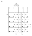
- FIG. 3 is an enlarged plan view of a panel of the liquid crystal display of FIG. 1 according to an exemplary embodiment of the present invention.
- the panel 100 includes the color photoresists 112b, the photo spacers 115, the first transparent electrodes 116, and the second transparent electrodes 122.
- the color photoresists 112b include an R photoresist, a G photoresist, and a B photoresist, and are arranged in a plurality of lines of rows in the color filter 112.
- the black matrices 112a are disposed between the color photoresists 112b.
- a pixel 150 of the panel 100 includes the R photoresist, the G photoresist, and the B photoresist. That is, one pixel 150 includes three photoresists.
- the photo spacers 115 are formed in some of regions where the black matrices 112a are formed.
- the B photoresists are formed smaller than the R photoresists and the G photoresists.
- the photo spacers 115 are formed in the black matrices 112a that are generated by the B photoresists that are relatively small.
- the present invention is not limited to regions where the photo spacers 115 are formed. That is, the photo spacers 115 can be formed in any regions of the black matrices 112a.
- the photo spacers 115 are formed adjacent the pixels 150, respectively. However, the present invention is not limited to a number of photo spacers 115 corresponding to the number of pixels 150.
- the first transparent electrodes 116 are arranged in a first direction to cover the color photoresists 112b of the color filter 112.
- the first transparent electrodes 116 are arranged in a column direction, they may be formed in a row direction. If the first transparent electrodes 116 are formed in the row direction, the second transparent electrodes 122 are formed in the column direction. If the first transparent electrodes 116 are formed in the column direction, the second transparent electrodes 122 may be formed in the row direction. That is, the first transparent electrodes 116 and the second transparent electrodes 122 are perpendicular to each other. Areas where the first transparent electrodes 116 and the second transparent electrodes 122 cross each other are the pixels 150.
- the second transparent electrodes 122 are arranged in a second direction perpendicular to the first direction that the first transparent electrodes 116 are arranged.
- the second transparent electrodes 122 include second R transparent electrodes 122R that are arranged in the second direction to cover the upper surface of the R photoresists, second G transparent electrodes 122G that are arranged in the second direction to cover the upper surface of the G photoresists, and second B transparent electrodes 122B that are arranged in the second direction to cover the upper surface of the B photoresists.
- the second direction is a row direction
- the second transparent electrodes 122 may be formed in a column direction.
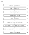
- FIG. 4 is a flowchart illustrating a method of manufacturing the liquid crystal display of FIG. 2B according to an exemplary embodiment of the present invention.
- the method includes the sequence of operations of: preparing a first substrate (S1), forming a color filter (S2), forming an overcoat layer (S3), forming an insulation film (S4), forming photo spacers (S5), forming first transparent electrodes (S6), patterning the first transparent electrodes (S7), combining a second substrate to the first substrate (S8), and injecting liquid crystal (S9).
- FIGS. 5a through 5i are cross-sectional views are cross-sectional views of the liquid crystal display of FIG. 2b as manufactured in accordance with the sequence depicted in FIG. 4 .
- the first substrate 111 in the operation of preparing a first substrate (S1), the first substrate 111, having a first surface 111 a that is approximately or wholly flat and a second surface 111 b that is an opposite to the first surface 111 a and is approximately or wholly flat, is prepared.
- the first substrate 111 may be formed of soda lime glass, of neutral borosilicate glass, of non-alkali glass, or an equivalent thereof according to the chemical composition of the glass.
- the present invention is not limited thereto.
- the black matrices 112a are formed by depositing a light blocking material on, preferably directly on, the first surface 111 a of the first substrate 111, patterning the first substrate 111 using an exposure and developing process, and hardening the first substrate 111.
- the light blocking material may be formed of resin, of chrome, of carbon black, of titanium oxide, or an equivalent thereof.
- the present invention is not limited thereto.
- the color photoresists 112b are formed by sequentially coating light reducing films including pigments expressing colors on the pixels 150 where the black matrices 112a are not formed, performing the exposure and developing process, and hardening the pixels 150, and then the color filter 112 is formed.
- the color photoresists 112b include the R photoresist, the G photoresist, and the B photoresist.
- the overcoat layer 113 is deposited on, preferably directly on, the color filter 112 to cover the color filter 112.
- the overcoat layer 113 flattens steps between the black matrices 112a and the color photoresists 112b when the color filter 112 is formed.
- the overcoat layer 113 may be formed of acrylic resin, or polyimide resin, or an equivalent thereof. However, the present invention is not limited thereto.
- the insulation film 114 is deposited on, preferably directly on, the overcoat layer 113 to cover the overcoat layer 113.
- the insulation film 114 may be formed using any one of selected from a thermal oxidation method, a chemical vapor deposition (CVD) method, an electrochemical oxidation method, or an equivalent thereof. However, the present invention is not limited thereto.
- the insulation film 114 may be formed of oxide SiO 2 or an equivalent thereof. However, the present invention is not limited thereto.
- the photo spacers 115 are formed at desired locations by photo spacer coating on, preferably directly on, the insulation film 114 to cover the insulation film 114 and performing exposure, developing, and etching processes.
- the photo spacers 115 are formed using photolithography, thereby preventing degradation of a display quality of the panel 100 due to leakage of light caused by undesired spacers formed on the color photoresists 112b.
- the photo spacers 115 are formed on or above regions of the black matrices 112a, i.e. entirely on the black matrices 112a such that the photo spacer 115 have no overlap with the color photoresists 112b.
- the first transparent electrodes 116 that are electrotype materials are formed on, preferably directly on, the insulation film 114 and the photo spacer 115 to cover the insulation film 114 and the photo spacers 115.
- the electrotype materials may be formed of indium tin oxide (ITO), of tin oxide (SnO 2 ), or an equivalent thereof.
- ITO indium tin oxide
- SnO 2 tin oxide
- the first transparent electrodes 116 may be formed using a screen printing method, an offset printing method, a photolithography method, or an equivalent method. However, the present invention is not limited thereto.
- the first transparent electrodes 116 are formed in a first direction by patterning the electrotype materials.
- the first transparent electrodes 116 formed on the upper surface and the side surface of the photo spacers 115 are removed. That is, the first transparent electrodes 116 are removed from the photo spacers 115 side surface such that the side surfaces of the first transparent electrodes 116 are spaced apart from the side surfaces of the photo spacers 115.
- the first transparent electrodes 116 are patterned using a photolithography process including photoresist coating, etching of the first transparent electrodes 116 by exposure and developing, and patterning.
- the present invention is not limited thereto.
- the second substrate unit 120 is closely combined to the first substrate unit 110 so that the first transparent electrodes 116 and the color filter 112 cross the second transparent electrodes 122 of the second substrate unit 120.
- a seal (not shown) is printed to make a frame receiving liquid crystal by adhering and fixing the first and second substrate units 110, 120.
- the first and second substrate units 110, 120 are combined using a vacuum method, a high temperature method, and a pressure method.
- the second substrate of the second substrate unit 120 may be formed of soda lime glass, of neutral borosilicate glass, of non-alkali glass, or an equivalent thereof according to the chemical composition of the glass.
- the present invention is not limited thereto.
- the second transparent electrodes 122 of the second substrate unit 120 can be formed and patterned using the same process as used to form and pattern the first transparent electrodes 116.
- the liquid crystal 130 is injected between the first substrate unit 110 and the second substrate unit 120.
- the liquid crystal 130 is filled within an empty space between the first substrate unit 110 and the second substrate unit 120.
- the liquid crystal 130 can be injected into an injection hole between the first substrate unit 110 and the second substrate 120 using a liquid crystal dispenser and then the injection hole is sealed.
- the present invention is not limited thereto.
- the method of manufacturing the liquid crystal display forms the first transparent electrodes 116 as a final process as compared to a conventional method of forming spacers after forming the first transparent electrodes 116, thereby reducing costs incurred in changing a process line for manufacturing a panel of the liquid crystal display and more stably manufacturing the panel than the conventional method.
- the photo spacers 115 are formed before the first transparent electrodes 115 are formed, i.e. the first transparent electrodes 115 are formed after the photo spacers 115, thereby forming the photo spacers 115 using a photolithography process in the same process line as the process line of forming the first substrate unit 110 before the photo spacers 115 are formed.
- the liquid crystal display and the manufacturing method thereof according to the present invention form a spacer in black matrix regions using a photolithography process, so that the spacer are not formed in color photoresist regions, thereby preventing degradation of a display quality due to leakage of light.
- the liquid crystal display and the manufacturing method thereof according to the present invention form transparent electrodes at a final process of manufacturing a panel, thereby reducing costs incurred in a change of a processing line and stably manufacturing the panel.
Landscapes
- Physics & Mathematics (AREA)
- Nonlinear Science (AREA)
- Mathematical Physics (AREA)
- Chemical & Material Sciences (AREA)
- Crystallography & Structural Chemistry (AREA)
- General Physics & Mathematics (AREA)
- Optics & Photonics (AREA)
- Geometry (AREA)
- Liquid Crystal (AREA)
- Optical Filters (AREA)
Applications Claiming Priority (1)
| Application Number | Priority Date | Filing Date | Title |
|---|---|---|---|
| KR1020080008689A KR100933867B1 (ko) | 2008-01-28 | 2008-01-28 | 액정 표시 장치 및 그의 제조 방법 |
Publications (1)
| Publication Number | Publication Date |
|---|---|
| EP2083317A1 true EP2083317A1 (de) | 2009-07-29 |
Family
ID=40561733
Family Applications (1)
| Application Number | Title | Priority Date | Filing Date |
|---|---|---|---|
| EP09151321A Withdrawn EP2083317A1 (de) | 2008-01-28 | 2009-01-26 | Flüssigkristallanzeige und Herstellungsverfahren dafür |
Country Status (5)
| Country | Link |
|---|---|
| US (1) | US20090190075A1 (de) |
| EP (1) | EP2083317A1 (de) |
| JP (1) | JP2009175732A (de) |
| KR (1) | KR100933867B1 (de) |
| CN (1) | CN101498855A (de) |
Families Citing this family (2)
| Publication number | Priority date | Publication date | Assignee | Title |
|---|---|---|---|---|
| CN101458417B (zh) * | 2008-12-17 | 2012-10-10 | 康佳集团股份有限公司 | 一种显示面板 |
| JP5733065B2 (ja) * | 2011-07-07 | 2015-06-10 | 三菱電機株式会社 | 液晶表示パネルとその修復方法 |
Citations (3)
| Publication number | Priority date | Publication date | Assignee | Title |
|---|---|---|---|---|
| EP0992841A1 (de) * | 1997-06-13 | 2000-04-12 | Sekisui Chemical Co., Ltd. | Flüssigkristallanzeige und deren herstellungsverfahren |
| JP2001159755A (ja) * | 1999-05-10 | 2001-06-12 | Citizen Watch Co Ltd | 液晶表示装置及びその製造方法 |
| US20050110922A1 (en) * | 2003-11-24 | 2005-05-26 | Dong-Hoon Lee | Color filter panel and its fabrication method using back exposure |
Family Cites Families (13)
| Publication number | Priority date | Publication date | Assignee | Title |
|---|---|---|---|---|
| US110922A (en) * | 1871-01-10 | Improvement in street-lamps | ||
| US4448491A (en) * | 1979-08-08 | 1984-05-15 | Canon Kabushiki Kaisha | Image display apparatus |
| JPH05257014A (ja) * | 1990-11-21 | 1993-10-08 | Fuji Photo Film Co Ltd | 位相差フィルム及びそれを用いた液晶表示装置 |
| JP3999824B2 (ja) * | 1995-08-21 | 2007-10-31 | 東芝電子エンジニアリング株式会社 | 液晶表示素子 |
| JP2001183513A (ja) * | 1999-12-22 | 2001-07-06 | Hitachi Ltd | カラーフィルタおよびその製造方法、カラー液晶表示装置 |
| JP2001183648A (ja) * | 1999-12-24 | 2001-07-06 | Nec Corp | カラー液晶表示装置及びその製造方法 |
| JP2001296530A (ja) * | 2000-04-12 | 2001-10-26 | Seiko Epson Corp | 電気光学装置およびその製造方法 |
| JP3824889B2 (ja) * | 2000-07-14 | 2006-09-20 | セイコーエプソン株式会社 | カラーフィルタ基板及び液晶装置、並びにこれらの製造方法 |
| KR20020056711A (ko) * | 2000-12-29 | 2002-07-10 | 주식회사 현대 디스플레이 테크놀로지 | 액정표시소자의 제조방법 |
| JP4048085B2 (ja) | 2002-07-24 | 2008-02-13 | 住友化学株式会社 | 液晶用カラーフィルター及びその製造方法 |
| JP2005134543A (ja) * | 2003-10-29 | 2005-05-26 | Seiko Epson Corp | 電気光学装置用基板の検査方法、及び電気光学装置用基板の製造方法。 |
| JP2006267782A (ja) * | 2005-03-25 | 2006-10-05 | Sanyo Epson Imaging Devices Corp | 電気光学装置及び電子機器 |
| JP2007206352A (ja) | 2006-02-01 | 2007-08-16 | Kyodo Printing Co Ltd | 液晶表示装置用素子基板の製造方法と液晶表示装置及びその製造方法 |
-
2008
- 2008-01-28 KR KR1020080008689A patent/KR100933867B1/ko not_active IP Right Cessation
- 2008-12-22 US US12/341,816 patent/US20090190075A1/en not_active Abandoned
-
2009
- 2009-01-09 JP JP2009003848A patent/JP2009175732A/ja active Pending
- 2009-01-23 CN CNA2009100009772A patent/CN101498855A/zh active Pending
- 2009-01-26 EP EP09151321A patent/EP2083317A1/de not_active Withdrawn
Patent Citations (3)
| Publication number | Priority date | Publication date | Assignee | Title |
|---|---|---|---|---|
| EP0992841A1 (de) * | 1997-06-13 | 2000-04-12 | Sekisui Chemical Co., Ltd. | Flüssigkristallanzeige und deren herstellungsverfahren |
| JP2001159755A (ja) * | 1999-05-10 | 2001-06-12 | Citizen Watch Co Ltd | 液晶表示装置及びその製造方法 |
| US20050110922A1 (en) * | 2003-11-24 | 2005-05-26 | Dong-Hoon Lee | Color filter panel and its fabrication method using back exposure |
Also Published As
| Publication number | Publication date |
|---|---|
| JP2009175732A (ja) | 2009-08-06 |
| KR100933867B1 (ko) | 2009-12-24 |
| KR20090082753A (ko) | 2009-07-31 |
| CN101498855A (zh) | 2009-08-05 |
| US20090190075A1 (en) | 2009-07-30 |
Similar Documents
| Publication | Publication Date | Title |
|---|---|---|
| US7656496B2 (en) | Liquid crystal display device and method for fabricating the same | |
| US7561245B2 (en) | Liquid crystal display device and method of fabricating the same | |
| US7821612B2 (en) | Color filter array panel and liquid crystal display including the same | |
| US7852450B2 (en) | Liquid crystal display device and method of fabricating the same | |
| US20090305444A1 (en) | Liquid crystal display device and method for fabricating the same | |
| US8514360B2 (en) | LCD device | |
| US20090258451A1 (en) | Liquid crystal display device | |
| KR100640216B1 (ko) | 액정 표시패널 및 그 제조방법 | |
| US20060170857A1 (en) | Liquid crystal display device | |
| JP2010039187A (ja) | 表示素子 | |
| US7248312B2 (en) | Liquid crystal display panel and fabricating method thereof | |
| US5847793A (en) | Liquid crystal display apparatus and fabrication process thereof | |
| EP2083317A1 (de) | Flüssigkristallanzeige und Herstellungsverfahren dafür | |
| KR100780831B1 (ko) | 표시소자 | |
| KR100603669B1 (ko) | 액정표시장치 및 그 제조방법 | |
| JP2002148624A (ja) | 液晶表示素子及びカラーフィルター及びそれらの製造方法 | |
| KR20050114123A (ko) | 액정 표시패널 및 그 제조방법 | |
| KR20040012309A (ko) | 패턴드 스페이서가 사용된 액정패널 | |
| KR20130066917A (ko) | 합착키를 구비한 프린지 필드형 액정표시장치 및 이를 이용한 프린지 필드형 액정표시장치의 제조방법 | |
| KR100928483B1 (ko) | 멀티도메인 액정표시장치의 제조 방법 | |
| KR20060093971A (ko) | 액정표시패널 및 그 제조방법 | |
| KR100628273B1 (ko) | 횡전계 방식의 액정표시장치 및 그의 제조방법 | |
| KR20060031336A (ko) | 패턴드 스페이서를 갖는 액정표시장치 | |
| KR100959777B1 (ko) | 액정 표시 패널의 제조 방법 | |
| KR19980041101A (ko) | 강유전성 액정표시장치 및 그 제조방법 |
Legal Events
| Date | Code | Title | Description |
|---|---|---|---|
| PUAI | Public reference made under article 153(3) epc to a published international application that has entered the european phase |
Free format text: ORIGINAL CODE: 0009012 |
|
| 17P | Request for examination filed |
Effective date: 20090126 |
|
| AK | Designated contracting states |
Kind code of ref document: A1 Designated state(s): AT BE BG CH CY CZ DE DK EE ES FI FR GB GR HR HU IE IS IT LI LT LU LV MC MK MT NL NO PL PT RO SE SI SK TR |
|
| AX | Request for extension of the european patent |
Extension state: AL BA RS |
|
| AKX | Designation fees paid |
Designated state(s): DE FR GB |
|
| STAA | Information on the status of an ep patent application or granted ep patent |
Free format text: STATUS: THE APPLICATION IS DEEMED TO BE WITHDRAWN |
|
| 18D | Application deemed to be withdrawn |
Effective date: 20120801 |