EP2074874B1 - Elektronisches gerät mit einer äusseren oberfläche mit zwei funktionen - Google Patents
Elektronisches gerät mit einer äusseren oberfläche mit zwei funktionen Download PDFInfo
- Publication number
- EP2074874B1 EP2074874B1 EP07735565A EP07735565A EP2074874B1 EP 2074874 B1 EP2074874 B1 EP 2074874B1 EP 07735565 A EP07735565 A EP 07735565A EP 07735565 A EP07735565 A EP 07735565A EP 2074874 B1 EP2074874 B1 EP 2074874B1
- Authority
- EP
- European Patent Office
- Prior art keywords
- areas
- electronic device
- thermally conductive
- layer
- uneven surface
- Prior art date
- Legal status (The legal status is an assumption and is not a legal conclusion. Google has not performed a legal analysis and makes no representation as to the accuracy of the status listed.)
- Ceased
Links
Images


Classifications
-
- H—ELECTRICITY
- H05—ELECTRIC TECHNIQUES NOT OTHERWISE PROVIDED FOR
- H05K—PRINTED CIRCUITS; CASINGS OR CONSTRUCTIONAL DETAILS OF ELECTRIC APPARATUS; MANUFACTURE OF ASSEMBLAGES OF ELECTRICAL COMPONENTS
- H05K5/00—Casings, cabinets or drawers for electric apparatus
- H05K5/02—Details
- H05K5/0209—Thermal insulation, e.g. for fire protection or for fire containment or for high temperature environments
-
- H—ELECTRICITY
- H05—ELECTRIC TECHNIQUES NOT OTHERWISE PROVIDED FOR
- H05K—PRINTED CIRCUITS; CASINGS OR CONSTRUCTIONAL DETAILS OF ELECTRIC APPARATUS; MANUFACTURE OF ASSEMBLAGES OF ELECTRICAL COMPONENTS
- H05K5/00—Casings, cabinets or drawers for electric apparatus
- H05K5/02—Details
-
- G—PHYSICS
- G06—COMPUTING OR CALCULATING; COUNTING
- G06F—ELECTRIC DIGITAL DATA PROCESSING
- G06F1/00—Details not covered by groups G06F3/00 - G06F13/00 and G06F21/00
- G06F1/16—Constructional details or arrangements
- G06F1/20—Cooling means
- G06F1/203—Cooling means for portable computers, e.g. for laptops
-
- H—ELECTRICITY
- H05—ELECTRIC TECHNIQUES NOT OTHERWISE PROVIDED FOR
- H05K—PRINTED CIRCUITS; CASINGS OR CONSTRUCTIONAL DETAILS OF ELECTRIC APPARATUS; MANUFACTURE OF ASSEMBLAGES OF ELECTRICAL COMPONENTS
- H05K7/00—Constructional details common to different types of electric apparatus
- H05K7/20—Modifications to facilitate cooling, ventilating, or heating
- H05K7/2039—Modifications to facilitate cooling, ventilating, or heating characterised by the heat transfer by conduction from the heat generating element to a dissipating body
- H05K7/20409—Outer radiating structures on heat dissipating housings, e.g. fins integrated with the housing
- H05K7/20418—Outer radiating structures on heat dissipating housings, e.g. fins integrated with the housing the radiating structures being additional and fastened onto the housing
Definitions
- Implementations described herein relate generally to electronic devices and, more particularly, to heat dissipating surfaces of electronic devices.
- Electronic devices such as mobile phones, media players, navigational devices, laptop computers, and hand held computers are becoming increasingly useful as technology shrinks the size and increases the computational power of such devices. All electronic devices require power to operate, some of which is given off as heat.
- Heat sinks may be used in electronic devices to help dissipate heat into the ambient atmosphere.
- the electronic devices, and in particular, the surface of the heat sink surface can become uncomfortably hot for the user.
- a device has an outer surface and includes a thermally conductive layer and second layer areas.
- the thermally conductive layer has an uneven surface and at least one other surface that is thermally coupled to a heat source.
- the uneven surface includes first areas that are higher than other areas of the uneven surface and further includes the second layer areas located on the first areas of the thermally conductive surface.
- the second layer areas of the device may be non-thermally conductive areas.
- the second layer areas of the device may include a plastic material or an elastomer.
- the thermally conductive layer may include a metal.
- the thermally conductive layer may act as a heat sink for the device.
- the uneven surface of the thermally conductive layer includes a wave like contour.
- the uneven surface of the thermally conductive includes a hill like contour or a box like contour.
- the second layer areas are formed of a material that is relatively easy to grip.
- the first areas of the uneven surface are separated from the low areas of the uneven surface by approximately 0.2 millimeters to on the order of a few millimeters.
- an electronic device in yet another aspect, includes a heat source and an outer surface portion.
- the outer surface portion includes a thermally conductive layer having an uneven surface and at least one other surface that is thermally coupled to the heat source.
- the uneven surface includes a plurality of raised areas.
- the outer surface portion includes a number of second layer areas located on the raised areas of the thermally conductive surface.
- the electronic device is a mobile terminal or a portable computer.
- the second layer areas of the electronic device include non-thermally conductive areas.
- the plurality of second layer areas of the electronic device each include a plastic material or an elastomer.
- the thermally conductive layer includes a metal.
- the uneven surface includes a wave like contour.
- the uneven surface may alternatively include a hill like contour or a box like contour.
- the plurality of second layer areas may be formed of a material that is relatively easy to grip.
- a dual function surface comprises means for dispersing heat, the means for dispersing heat having a thermally conductive uneven surface.
- the dual function surface further comprises means for insulating portions of the uneven surface with a material that is relatively non-thermally conductive.
- the means for insulating portions of the uneven surface has a high coefficient of friction and a pleasant tactile feel.
- the uneven surface has a wave contour.
- an outer portion of an electronic device is given an uneven profile, such as a wavy profile, to aid in the dissipation of heat.
- the high points in the uneven profile, such as the peaks of the wavy profile may be stamped or coated with a non-thermal conductive coating.
- the non-thermal conductive coating may be relatively pleasant to user touch. In this manner, the uneven profile portion of the electronic device functions to both dissipate heat while allowing the user to comfortably touch or hold the device.
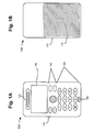
- Figs. 1A and 1B are front side and back side views, respectively, of an exemplary electronic device 100.
- electronic device 100 is a mobile terminal. More generally, it can be appreciated that electronic device 100 can be any type of electronic device.
- Device 100 may include housing 110, speaker 120, display 130, control keys 140, keypad 150, and microphone 160.
- Housing 110 may protect the components of device 100 from outside elements.
- Housing 110 may be made from thermoplastics, metals, elastomers (e.g., synthetic rubber and/or natural rubber), and/or other similar materials.
- Speaker 120 may provide audible information to a user of device 100.
- Display 130 may provide visual information to the user. For example, display 130 may provide information regarding incoming or outgoing telephone calls, games, telephone numbers, the current time, e-mail, etc.
- Control keys 140 may permit the user to interact with device 100 to cause device 100 to perform one or more operations.
- Keypad 150 may include a standard telephone keypad and may include additional keys to enable typing information into device 100.
- Microphone 160 may receive audible information from the user.
- housing 110 of device 100 may include an uneven surface portion, referred to as a dual function surface 115 herein.
- dual function surface 115 is implemented on the back side of device 100.
- Dual function surface 115 is designed to dissipate heat while having a surface that is pleasant for the user to touch.
- Dual function surface 115 may generally be implemented on any external surface of housing 110, and can be particularly useful when implemented on areas of housing 110 from which it is desirable to dissipate heat, such as over a battery charging area or over an area an covers core circuitry of device 100.
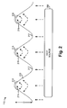
- Fig. 2 is a diagram illustrating a cross-section of an exemplary implementation of dual function surface 115.
- dual function surface 115 is shown as having a "wavy" or wave-like profile that includes peak portions 216 that are higher than valley portions 217.
- the wavy profile may be formed by thermally conductive layer 210.
- Layer 210 may be made from, for example, a thermally conductive metal or other material.
- Layer 210 may generally operate to dissipate heat into the ambient atmosphere through the surface of layer 210.
- layer 210 may operate as a heat sink in which a top surface contacts the outside atmosphere and another surface is in contact with, or thermally coupled to, a heat source 250 that is to be dissipated.
- Heat source 250 may include internal heat producing elements of device 100, such as electronic circuitry. As conceptually shown via the dashed arrows in Fig. 2 , heat generated by heat source 250 may move to the cooler outer surface of device 100 via layer 210.
- the uneven profile of the top surface of layer 210 provides a relatively large surface area for dissipating heat.
- the surface area of the top surface of layer 210 may be larger than if layer 210 was constructed as a flat surface, thus providing additional ventilation surface for heat exchange.
- the top surface of layer 210 may be stamped or coated with non-thermal conductive areas 215.
- non-thermal conductive areas 215 may be located at or near the peaks of layer 210 (i.e., near peak portions 216).
- Non-thermal conductive areas 215 may, for example, be implemented as a plastic material (e.g., a thermoplastic) or as an elastomer (e.g., rubber).
- the material may be selected as a material that is relatively non-thennally conductive and has a pleasing tactile feel and/or has a high coefficient of static or dynamic friction (i.e., it's "grippy").
- the total area covered by the non-thermal conductive areas 215 may be less, and in some implementations, significantly less than the total area covered by dual function surface 115.
- Making layer 210 uneven serves to increase the available outer surface, for improved thermal exchange, and create a relief that allows for non-thermal conductive areas 215 to be simply added.
- the amplitude of the waves of layer 210 may vary based on the design of the particular device, and may typically vary from the order of a few tenths of a millimeter to a few millimeters.
- the amplitude, shown as distance "D" in Fig. 2 may range from approximately 0.2 - 0.5 millimeters to a few millimeters or greater (e.g., 3 millimeters or more).
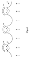
- Fig. 3 is a diagram conceptually illustrating the exemplary implementation of dual function surface 115, as shown in Fig. 2 , when in use by an operator.
- curve 320 represents an outline of a human hand touching (e.g., holding) electronic device 100 on dual function surface 115.
- the hand may tend to naturally contact non-thermal conductive areas 215, which may provide a pleasant tactile response/feel while providing shielding from the heat of layer 210.
- non-thennal conductive area 215 may be designed so that it is physically very difficult or unlikely for the operator's hand to contact layer 210. In other applications, it may be acceptable if some portion of the operator's hand comes into contact with layer 210. In other words, in some applications, non-thermal conductive area 215 may provide acceptable results without acting as a complete physical separator between the operator's hand and layer 210.
- Dual function surface 115 includes a thermally conductive layer 210 that includes uneven portions that are capped or topped by non-thermal conductive areas 215.
- the tops provided by non-thermal conductive areas 215 allow a user to hold electronic device 100 without actually contacting much or all of the heat dissipating portion of layer 210.
- waves in dual function surface 115 provide for greater ventilation than a flat thermally conductive surface.
- manufacture of dual function surface 115 may be relatively simple and cheap to implement.
- non-thermal conductive areas 215 may be stamped or pressed onto layer 210.
- layer 210 may be a single continuous layer with the peak portions (i.e., portions 216) being made from a non-thermally conductive material and the remaining portions being made from a thermally conductive material.
- Fig. 4 is a cross-section diagram illustrating an alternate exemplary implementation of dual function surface 115.
- dual function surface 115 includes a "hilly" profile.
- the hilly profile is formed by a thermally conductive layer 410.
- Thermally conductive layer 410 may be made of materials similar to and functions in a manner similar to layer 210 (described above).
- Layer 410 may be stamped or coated with non-thermal conductive areas 415.
- Non-thennal conductive areas 415 function similarly to non-thermal conductive areas 215 (described above). That is, non-thermal conductive areas 415 may be located at or near the top of layer 410 and be selected as a material that is relatively non-thermally conductive and that has a pleasing tactile feel and/or is relatively easy to grip.
- Fig. 5 is a cross-section diagram illustrating another alternate exemplary implementation of dual function surface 115.
- dual function surface 115 has a "boxy" profile.
- the boxy profile is formed by a thermally conductive layer 510.
- Thermally conductive layer 510 may be made of materials similar to and functions in a manner similar to layer 210 (described above).
- Layer 510 may be stamped or coated with non-thermal conductive areas 515.
- Non-thermal conductive areas 515 function similarly to non-thermal conductive areas 215 (described above). That is, non-thermal conductive areas 515 may be located at or near the top of layer 510 and be selected as a material that is relatively non-thermally conductive and that has a pleasing tactile feel and/or is relatively easy to grip/hold.
- dual function surface 115 is shown in Fig. 1B as being implemented in mobile terminal 100, it can be appreciated that dual function surface 115 could be implemented with any electronic device.
- Fig. 6 is a diagram illustrating another exemplary electronic device in which the dual function surface is implemented.
- a portable computer i.e., a laptop
- Portable computer 600 may include the dual function surface described above.
- Portable computer 600 may include, for example, a touch pad entry portion 601, a keyboard 602, and a display 603.
- portable computer 600 includes a dual function surface 615 (shown as the area including diagonal lines).
- Dual function surface 615 may be implemented as described above, such as the implementations shown in Figs. 2-5 .
- dual function surface 615 is located on a front portion of portable computer 600. It can be appreciated that in other implementations, dual function surface 615 may be located in other or in additional locations on portable computer 600, such as on a back or side surface of portable computer 600.
- a dual function surface acts as a heat sink to dissipate heat while also including relatively good tactile qualities.
Landscapes
- Engineering & Computer Science (AREA)
- Theoretical Computer Science (AREA)
- Physics & Mathematics (AREA)
- Human Computer Interaction (AREA)
- General Engineering & Computer Science (AREA)
- General Physics & Mathematics (AREA)
- Computer Hardware Design (AREA)
- Microelectronics & Electronic Packaging (AREA)
- Thermal Sciences (AREA)
- Cooling Or The Like Of Electrical Apparatus (AREA)
- Telephone Set Structure (AREA)
- Cooling Or The Like Of Semiconductors Or Solid State Devices (AREA)
- Switches That Are Operated By Magnetic Or Electric Fields (AREA)
- Measuring Pulse, Heart Rate, Blood Pressure Or Blood Flow (AREA)
- Steering Controls (AREA)
Claims (15)
- Äußere Oberfläche eines elektronischen Geräts (100), welche aufweist:eine wärmeleitfähige Schicht (210, 410, 510) mit einer unebenen Oberfläche und mindestens einer weiteren Oberfläche, welche thermisch mit einer Wärmequelle (250) gekoppelt ist, wobei die unebene Oberfläche mehrere erste Bereiche (216) aufweist, die höher sind als andere Bereiche der unebenen Oberfläche; undmehrere Bereiche einer zweiten Schicht (215, 415, 515), die nur auf den ersten Bereichen der unebenen Oberfläche angeordnet sind, wobei die mehreren Bereiche der zweiten Schicht (215, 415, 515) ein Kunststoffmaterial oder ein Elastomer enthalten.
- Äußere Oberfläche des elektronischen Geräts (100) nach Anspruch 1,
wobei die mehreren Bereiche (215, 415, 515) der zweiten Schicht nicht wärmeleitfähig sind. - Äußere Oberfläche des elektronischen Geräts (100) nach Anspruch 1,
wobei die wärmeleitfähige Schicht (210, 410, 510) ein Metall enthält. - Äußere Oberfläche des elektronischen Geräts (100) nach Anspruch 1,
wobei die wärmeleitfähige Schicht (210, 410, 510) als Wärmesenke für das Gerät dient. - Äußere Oberfläche des elektronischen Geräts (100) nach Anspruch 1,
wobei die Oberfläche der wärmeleitfähigen Schicht ein wellenförmiges Profil aufweist. - Äußere Oberfläche des elektronischen Geräts (100) nach Anspruch 1,
wobei die Oberfläche der wärmeleitfähigen Schicht ein hügel- oder kastenförmiges Profil aufweist. - Äußere Oberfläche des elektronischen Geräts (100) nach Anspruch 1,
wobei die ersten Bereiche (216) der unebenen Oberfläche in einem Abstand von rund 0,2 bis zu einigen Millimetern von den tiefer liegenden Bereichen der unebenen Oberfläche angeordnet sind. - Elektronisches Gerät (100), welches aufweist:eine Wärmequelle (250); undeinen äußeren Oberflächenteil (115) auseiner wärmeleitfähigen Schicht (210, 410, 510) mit einer unebenen Oberfläche und mindestens einer weiteren Oberfläche, welche thermisch mit einer Wärmequelle (250) gekoppelt ist, wobei die unebene Oberfläche mehrere erhöhte Bereiche (216) aufweist; undmehrere Bereiche einer zweiten Schicht (215, 415, 515), die nur auf den erhöhten Bereichen (216) der unebenen Oberfläche angeordnet sind, wobei die mehreren Bereiche der zweiten Schicht (215, 415, 515) jeweils ein Kunststoffmaterial oder ein Elastomer enthalten.
- Elektronisches Gerät (100) nach Anspruch 8,
wobei das elektronische Gerät (100) ein mobiles Endgerät oder ein tragbarer Computer ist. - Elektronisches Gerät (100) nach Anspruch 8,
wobei die mehreren Bereiche der zweiten Schicht (215, 415, 515) nicht wärmeleitfähige Bereiche aufweisen. - Elektronisches Gerät (100) nach Anspruch 10,
wobei die wärmeleitfähige Schicht (210, 410, 510) ein Metall enthält. - Elektronisches Gerät (100) nach Anspruch 8,
wobei die unebene Oberfläche ein wellenförmiges Profil aufweist. - Elektronisches Gerät (100) nach Anspruch 8,
wobei die unebene Oberfläche ein hügel- oder kastenförmiges Profil aufweist. - Elektronisches Gerät (100) nach Anspruch 8,
wobei die erhöhten Bereiche (216) der unebenen Oberfläche in einem Abstand von rund 0,2 bis zu einigen Millimetern von den tiefer liegenden Bereichen der unebenen Oberfläche angeordnet sind. - Doppelfunktionsoberfläche (115) eines elektronischen Geräts (100), welche aufweist:Mittel zur Wärmeabführung (210), welches eine wärmeleitfähige unebene Oberfläche mit mehreren erhöhten Bereichen aufweist; andMittel zur Isolierung nur der erhöhten Bereiche der unebenen Oberfläche (216) mittels eines Materials, das relativ nicht wärmeleitfähig ist, wo es ein Kunststoffmaterial oder ein Elastomer enthält.
Applications Claiming Priority (2)
| Application Number | Priority Date | Filing Date | Title |
|---|---|---|---|
| US11/550,915 US20080149320A1 (en) | 2006-10-19 | 2006-10-19 | Electronic device with dual function outer surface |
| PCT/IB2007/051431 WO2008047254A2 (en) | 2006-10-19 | 2007-04-19 | Electronic device with dual function outer surface |
Publications (2)
| Publication Number | Publication Date |
|---|---|
| EP2074874A2 EP2074874A2 (de) | 2009-07-01 |
| EP2074874B1 true EP2074874B1 (de) | 2010-02-03 |
Family
ID=39314422
Family Applications (1)
| Application Number | Title | Priority Date | Filing Date |
|---|---|---|---|
| EP07735565A Ceased EP2074874B1 (de) | 2006-10-19 | 2007-04-19 | Elektronisches gerät mit einer äusseren oberfläche mit zwei funktionen |
Country Status (8)
| Country | Link |
|---|---|
| US (1) | US20080149320A1 (de) |
| EP (1) | EP2074874B1 (de) |
| JP (1) | JP2010507243A (de) |
| KR (1) | KR101323975B1 (de) |
| CN (1) | CN101563965A (de) |
| AT (1) | ATE457121T1 (de) |
| DE (1) | DE602007004679D1 (de) |
| WO (1) | WO2008047254A2 (de) |
Cited By (1)
| Publication number | Priority date | Publication date | Assignee | Title |
|---|---|---|---|---|
| US12412807B2 (en) | 2019-12-06 | 2025-09-09 | 3M Innovative Properties Company | Patterned design for thermal management of two-phase immersion cooling system for electronics |
Families Citing this family (6)
| Publication number | Priority date | Publication date | Assignee | Title |
|---|---|---|---|---|
| US9165854B2 (en) * | 2012-04-12 | 2015-10-20 | Qualcomm Incorporated | Heat dissipation features, electronic devices incorporating heat dissipation features, and methods of making heat dissipation features |
| TWI472833B (zh) * | 2013-06-06 | 2015-02-11 | Innolux Corp | 顯示裝置 |
| TWI553258B (zh) * | 2013-07-15 | 2016-10-11 | 緯創資通股份有限公司 | 具有升降功能之腳墊機構及其電子裝置 |
| WO2016175779A1 (en) * | 2015-04-29 | 2016-11-03 | Hewlett-Packard Development Company, L.P. | Cover for devices |
| JP6495485B2 (ja) | 2016-02-05 | 2019-04-03 | クワントン オーピーピーオー モバイル テレコミュニケーションズ コーポレイション リミテッド | アダプター及び充電制御方法 |
| ES2829256T3 (es) * | 2016-02-05 | 2021-05-31 | Guangdong Oppo Mobile Telecommunications Corp Ltd | Método de carga y adaptador |
Family Cites Families (14)
| Publication number | Priority date | Publication date | Assignee | Title |
|---|---|---|---|---|
| US4182412A (en) * | 1978-01-09 | 1980-01-08 | Uop Inc. | Finned heat transfer tube with porous boiling surface and method for producing same |
| US4359086A (en) * | 1981-05-18 | 1982-11-16 | The Trane Company | Heat exchange surface with porous coating and subsurface cavities |
| US4819719A (en) * | 1987-01-20 | 1989-04-11 | Mcdonnell Douglas Corporation | Enhanced evaporator surface |
| US4838347A (en) * | 1987-07-02 | 1989-06-13 | American Telephone And Telegraph Company At&T Bell Laboratories | Thermal conductor assembly |
| US5263773A (en) * | 1991-11-14 | 1993-11-23 | White Consolidated Industries, Inc. | Cabinet structure and method of producing same |
| US5550326A (en) * | 1994-07-13 | 1996-08-27 | Parker-Hannifin Corporation | Heat dissipator for electronic components |
| JP3106120B2 (ja) * | 1997-05-16 | 2000-11-06 | 三菱電機株式会社 | 携帯型電子機器 |
| JPH11204949A (ja) * | 1998-01-13 | 1999-07-30 | Fujitsu Ltd | 電子機器筐体構造 |
| JP2000148306A (ja) * | 1998-11-06 | 2000-05-26 | Matsushita Electric Ind Co Ltd | 電子機器筐体構造 |
| TW553822B (en) * | 2000-11-22 | 2003-09-21 | Matsushita Electric Industrial Co Ltd | Magnesium alloy moldings and method for manufacturing thereof |
| US6519157B1 (en) * | 2001-10-23 | 2003-02-11 | Nlight Photonics Corporation | System and method for mounting a stack-up structure |
| TWI257543B (en) * | 2003-07-02 | 2006-07-01 | Delta Electronics Inc | Equalizing temperature device |
| PT2498572T (pt) * | 2004-02-05 | 2019-06-14 | Worldbest Corp | Aparelho radiador |
| JP2007042863A (ja) * | 2005-08-03 | 2007-02-15 | Matsushita Electric Ind Co Ltd | 電子機器 |
-
2006
- 2006-10-19 US US11/550,915 patent/US20080149320A1/en not_active Abandoned
-
2007
- 2007-04-19 DE DE602007004679T patent/DE602007004679D1/de active Active
- 2007-04-19 KR KR1020097010169A patent/KR101323975B1/ko not_active Expired - Fee Related
- 2007-04-19 EP EP07735565A patent/EP2074874B1/de not_active Ceased
- 2007-04-19 AT AT07735565T patent/ATE457121T1/de not_active IP Right Cessation
- 2007-04-19 JP JP2009532918A patent/JP2010507243A/ja active Pending
- 2007-04-19 CN CNA2007800474241A patent/CN101563965A/zh active Pending
- 2007-04-19 WO PCT/IB2007/051431 patent/WO2008047254A2/en not_active Ceased
Cited By (1)
| Publication number | Priority date | Publication date | Assignee | Title |
|---|---|---|---|---|
| US12412807B2 (en) | 2019-12-06 | 2025-09-09 | 3M Innovative Properties Company | Patterned design for thermal management of two-phase immersion cooling system for electronics |
Also Published As
| Publication number | Publication date |
|---|---|
| WO2008047254A3 (en) | 2008-10-30 |
| DE602007004679D1 (de) | 2010-03-25 |
| JP2010507243A (ja) | 2010-03-04 |
| KR20090071647A (ko) | 2009-07-01 |
| KR101323975B1 (ko) | 2013-10-31 |
| US20080149320A1 (en) | 2008-06-26 |
| WO2008047254A2 (en) | 2008-04-24 |
| ATE457121T1 (de) | 2010-02-15 |
| EP2074874A2 (de) | 2009-07-01 |
| CN101563965A (zh) | 2009-10-21 |
Similar Documents
| Publication | Publication Date | Title |
|---|---|---|
| EP2074874B1 (de) | Elektronisches gerät mit einer äusseren oberfläche mit zwei funktionen | |
| US6552899B2 (en) | Mobile computer | |
| US20130077233A1 (en) | Electronic device | |
| WO2007029311A1 (ja) | 電子機器 | |
| US9430006B1 (en) | Computing device with heat spreader | |
| US20140110083A1 (en) | Heat dissipating protective cover | |
| CN101657870A (zh) | 键盘、按压式开关及具备该开关的电子设备 | |
| JP2010055642A (ja) | 電子機器 | |
| US11330734B2 (en) | Case assembly and electronic device | |
| WO2007074547A1 (ja) | 押圧式スイッチ及びこれを備えた電子機器 | |
| WO2025235112A1 (en) | Computing device case | |
| TW200900902A (en) | Computer accessory device having recess for airflow | |
| TWM442684U (en) | Heat dissipation protective jacket | |
| CN222216343U (zh) | 电子设备 | |
| JP5028650B2 (ja) | 携帯電話装置 | |
| JP2010170047A (ja) | 携帯型電子機器 | |
| JP2007250725A (ja) | 携帯端末装置 | |
| TW201620368A (zh) | 具散熱之保護裝置 | |
| US20250348113A1 (en) | Computing device case | |
| CN214627766U (zh) | 散热结构和电子设备 | |
| CN212659465U (zh) | 键盘及电子设备 | |
| US20250349477A1 (en) | Computing device case | |
| US12328845B2 (en) | Thermal conduit for electronic device | |
| CN211321375U (zh) | 电子产品保护壳 | |
| KR20260005009A (ko) | 열 계면 부재 및 이를 포함하는 전자 장치 |
Legal Events
| Date | Code | Title | Description |
|---|---|---|---|
| PUAI | Public reference made under article 153(3) epc to a published international application that has entered the european phase |
Free format text: ORIGINAL CODE: 0009012 |
|
| 17P | Request for examination filed |
Effective date: 20090417 |
|
| AK | Designated contracting states |
Kind code of ref document: A2 Designated state(s): AT BE BG CH CY CZ DE DK EE ES FI FR GB GR HU IE IS IT LI LT LU LV MC MT NL PL PT RO SE SI SK TR |
|
| GRAP | Despatch of communication of intention to grant a patent |
Free format text: ORIGINAL CODE: EPIDOSNIGR1 |
|
| RIN1 | Information on inventor provided before grant (corrected) |
Inventor name: NILSSON, KRISTER Inventor name: HUGOSSON, MARIA Inventor name: KARLELID, TORBJORN Inventor name: TAKAMOTO, TARO Inventor name: RYDEN, ANDREAS Inventor name: VANTU, FLORIN |
|
| GRAS | Grant fee paid |
Free format text: ORIGINAL CODE: EPIDOSNIGR3 |
|
| GRAA | (expected) grant |
Free format text: ORIGINAL CODE: 0009210 |
|
| DAX | Request for extension of the european patent (deleted) | ||
| AK | Designated contracting states |
Kind code of ref document: B1 Designated state(s): AT BE BG CH CY CZ DE DK EE ES FI FR GB GR HU IE IS IT LI LT LU LV MC MT NL PL PT RO SE SI SK TR |
|
| REG | Reference to a national code |
Ref country code: GB Ref legal event code: FG4D |
|
| REG | Reference to a national code |
Ref country code: CH Ref legal event code: EP |
|
| REG | Reference to a national code |
Ref country code: IE Ref legal event code: FG4D |
|
| REF | Corresponds to: |
Ref document number: 602007004679 Country of ref document: DE Date of ref document: 20100325 Kind code of ref document: P |
|
| REG | Reference to a national code |
Ref country code: NL Ref legal event code: VDEP Effective date: 20100203 |
|
| LTIE | Lt: invalidation of european patent or patent extension |
Effective date: 20100203 |
|
| PG25 | Lapsed in a contracting state [announced via postgrant information from national office to epo] |
Ref country code: IS Free format text: LAPSE BECAUSE OF FAILURE TO SUBMIT A TRANSLATION OF THE DESCRIPTION OR TO PAY THE FEE WITHIN THE PRESCRIBED TIME-LIMIT Effective date: 20100603 Ref country code: LT Free format text: LAPSE BECAUSE OF FAILURE TO SUBMIT A TRANSLATION OF THE DESCRIPTION OR TO PAY THE FEE WITHIN THE PRESCRIBED TIME-LIMIT Effective date: 20100203 Ref country code: PT Free format text: LAPSE BECAUSE OF FAILURE TO SUBMIT A TRANSLATION OF THE DESCRIPTION OR TO PAY THE FEE WITHIN THE PRESCRIBED TIME-LIMIT Effective date: 20100603 Ref country code: ES Free format text: LAPSE BECAUSE OF FAILURE TO SUBMIT A TRANSLATION OF THE DESCRIPTION OR TO PAY THE FEE WITHIN THE PRESCRIBED TIME-LIMIT Effective date: 20100514 |
|
| PG25 | Lapsed in a contracting state [announced via postgrant information from national office to epo] |
Ref country code: FI Free format text: LAPSE BECAUSE OF FAILURE TO SUBMIT A TRANSLATION OF THE DESCRIPTION OR TO PAY THE FEE WITHIN THE PRESCRIBED TIME-LIMIT Effective date: 20100203 Ref country code: AT Free format text: LAPSE BECAUSE OF FAILURE TO SUBMIT A TRANSLATION OF THE DESCRIPTION OR TO PAY THE FEE WITHIN THE PRESCRIBED TIME-LIMIT Effective date: 20100203 Ref country code: LV Free format text: LAPSE BECAUSE OF FAILURE TO SUBMIT A TRANSLATION OF THE DESCRIPTION OR TO PAY THE FEE WITHIN THE PRESCRIBED TIME-LIMIT Effective date: 20100203 Ref country code: SI Free format text: LAPSE BECAUSE OF FAILURE TO SUBMIT A TRANSLATION OF THE DESCRIPTION OR TO PAY THE FEE WITHIN THE PRESCRIBED TIME-LIMIT Effective date: 20100203 Ref country code: PL Free format text: LAPSE BECAUSE OF FAILURE TO SUBMIT A TRANSLATION OF THE DESCRIPTION OR TO PAY THE FEE WITHIN THE PRESCRIBED TIME-LIMIT Effective date: 20100203 |
|
| PG25 | Lapsed in a contracting state [announced via postgrant information from national office to epo] |
Ref country code: SE Free format text: LAPSE BECAUSE OF FAILURE TO SUBMIT A TRANSLATION OF THE DESCRIPTION OR TO PAY THE FEE WITHIN THE PRESCRIBED TIME-LIMIT Effective date: 20100203 Ref country code: BE Free format text: LAPSE BECAUSE OF FAILURE TO SUBMIT A TRANSLATION OF THE DESCRIPTION OR TO PAY THE FEE WITHIN THE PRESCRIBED TIME-LIMIT Effective date: 20100203 Ref country code: CY Free format text: LAPSE BECAUSE OF FAILURE TO SUBMIT A TRANSLATION OF THE DESCRIPTION OR TO PAY THE FEE WITHIN THE PRESCRIBED TIME-LIMIT Effective date: 20100203 Ref country code: EE Free format text: LAPSE BECAUSE OF FAILURE TO SUBMIT A TRANSLATION OF THE DESCRIPTION OR TO PAY THE FEE WITHIN THE PRESCRIBED TIME-LIMIT Effective date: 20100203 Ref country code: GR Free format text: LAPSE BECAUSE OF FAILURE TO SUBMIT A TRANSLATION OF THE DESCRIPTION OR TO PAY THE FEE WITHIN THE PRESCRIBED TIME-LIMIT Effective date: 20100504 Ref country code: NL Free format text: LAPSE BECAUSE OF FAILURE TO SUBMIT A TRANSLATION OF THE DESCRIPTION OR TO PAY THE FEE WITHIN THE PRESCRIBED TIME-LIMIT Effective date: 20100203 Ref country code: RO Free format text: LAPSE BECAUSE OF FAILURE TO SUBMIT A TRANSLATION OF THE DESCRIPTION OR TO PAY THE FEE WITHIN THE PRESCRIBED TIME-LIMIT Effective date: 20100203 |
|
| PG25 | Lapsed in a contracting state [announced via postgrant information from national office to epo] |
Ref country code: CZ Free format text: LAPSE BECAUSE OF FAILURE TO SUBMIT A TRANSLATION OF THE DESCRIPTION OR TO PAY THE FEE WITHIN THE PRESCRIBED TIME-LIMIT Effective date: 20100203 Ref country code: MC Free format text: LAPSE BECAUSE OF NON-PAYMENT OF DUE FEES Effective date: 20100430 Ref country code: SK Free format text: LAPSE BECAUSE OF FAILURE TO SUBMIT A TRANSLATION OF THE DESCRIPTION OR TO PAY THE FEE WITHIN THE PRESCRIBED TIME-LIMIT Effective date: 20100203 Ref country code: BG Free format text: LAPSE BECAUSE OF FAILURE TO SUBMIT A TRANSLATION OF THE DESCRIPTION OR TO PAY THE FEE WITHIN THE PRESCRIBED TIME-LIMIT Effective date: 20100503 |
|
| PLBE | No opposition filed within time limit |
Free format text: ORIGINAL CODE: 0009261 |
|
| STAA | Information on the status of an ep patent application or granted ep patent |
Free format text: STATUS: NO OPPOSITION FILED WITHIN TIME LIMIT |
|
| 26N | No opposition filed |
Effective date: 20101104 |
|
| PG25 | Lapsed in a contracting state [announced via postgrant information from national office to epo] |
Ref country code: IE Free format text: LAPSE BECAUSE OF NON-PAYMENT OF DUE FEES Effective date: 20100419 Ref country code: DK Free format text: LAPSE BECAUSE OF FAILURE TO SUBMIT A TRANSLATION OF THE DESCRIPTION OR TO PAY THE FEE WITHIN THE PRESCRIBED TIME-LIMIT Effective date: 20100203 |
|
| PG25 | Lapsed in a contracting state [announced via postgrant information from national office to epo] |
Ref country code: IT Free format text: LAPSE BECAUSE OF FAILURE TO SUBMIT A TRANSLATION OF THE DESCRIPTION OR TO PAY THE FEE WITHIN THE PRESCRIBED TIME-LIMIT Effective date: 20100203 |
|
| PG25 | Lapsed in a contracting state [announced via postgrant information from national office to epo] |
Ref country code: MT Free format text: LAPSE BECAUSE OF FAILURE TO SUBMIT A TRANSLATION OF THE DESCRIPTION OR TO PAY THE FEE WITHIN THE PRESCRIBED TIME-LIMIT Effective date: 20100203 |
|
| REG | Reference to a national code |
Ref country code: CH Ref legal event code: PL |
|
| PG25 | Lapsed in a contracting state [announced via postgrant information from national office to epo] |
Ref country code: LI Free format text: LAPSE BECAUSE OF NON-PAYMENT OF DUE FEES Effective date: 20110430 Ref country code: CH Free format text: LAPSE BECAUSE OF NON-PAYMENT OF DUE FEES Effective date: 20110430 |
|
| PG25 | Lapsed in a contracting state [announced via postgrant information from national office to epo] |
Ref country code: HU Free format text: LAPSE BECAUSE OF FAILURE TO SUBMIT A TRANSLATION OF THE DESCRIPTION OR TO PAY THE FEE WITHIN THE PRESCRIBED TIME-LIMIT Effective date: 20100804 Ref country code: LU Free format text: LAPSE BECAUSE OF NON-PAYMENT OF DUE FEES Effective date: 20100419 |
|
| PG25 | Lapsed in a contracting state [announced via postgrant information from national office to epo] |
Ref country code: TR Free format text: LAPSE BECAUSE OF FAILURE TO SUBMIT A TRANSLATION OF THE DESCRIPTION OR TO PAY THE FEE WITHIN THE PRESCRIBED TIME-LIMIT Effective date: 20100203 |
|
| REG | Reference to a national code |
Ref country code: FR Ref legal event code: PLFP Year of fee payment: 10 |
|
| REG | Reference to a national code |
Ref country code: FR Ref legal event code: PLFP Year of fee payment: 11 |
|
| REG | Reference to a national code |
Ref country code: FR Ref legal event code: PLFP Year of fee payment: 12 |
|
| PGFP | Annual fee paid to national office [announced via postgrant information from national office to epo] |
Ref country code: GB Payment date: 20180329 Year of fee payment: 12 |
|
| PGFP | Annual fee paid to national office [announced via postgrant information from national office to epo] |
Ref country code: FR Payment date: 20180326 Year of fee payment: 12 |
|
| PGFP | Annual fee paid to national office [announced via postgrant information from national office to epo] |
Ref country code: DE Payment date: 20180404 Year of fee payment: 12 |
|
| REG | Reference to a national code |
Ref country code: DE Ref legal event code: R119 Ref document number: 602007004679 Country of ref document: DE |
|
| GBPC | Gb: european patent ceased through non-payment of renewal fee |
Effective date: 20190419 |
|
| PG25 | Lapsed in a contracting state [announced via postgrant information from national office to epo] |
Ref country code: DE Free format text: LAPSE BECAUSE OF NON-PAYMENT OF DUE FEES Effective date: 20191101 Ref country code: GB Free format text: LAPSE BECAUSE OF NON-PAYMENT OF DUE FEES Effective date: 20190419 |
|
| PG25 | Lapsed in a contracting state [announced via postgrant information from national office to epo] |
Ref country code: FR Free format text: LAPSE BECAUSE OF NON-PAYMENT OF DUE FEES Effective date: 20190430 |