EP2074626B1 - Nichtflüchtiger speicher und verfahren für lineare schätzung der eingangsprogrammierungsspannung - Google Patents
Nichtflüchtiger speicher und verfahren für lineare schätzung der eingangsprogrammierungsspannung Download PDFInfo
- Publication number
- EP2074626B1 EP2074626B1 EP07841761A EP07841761A EP2074626B1 EP 2074626 B1 EP2074626 B1 EP 2074626B1 EP 07841761 A EP07841761 A EP 07841761A EP 07841761 A EP07841761 A EP 07841761A EP 2074626 B1 EP2074626 B1 EP 2074626B1
- Authority
- EP
- European Patent Office
- Prior art keywords
- page
- programming
- memory
- programming voltage
- block
- Prior art date
- Legal status (The legal status is an assumption and is not a legal conclusion. Google has not performed a legal analysis and makes no representation as to the accuracy of the status listed.)
- Not-in-force
Links
Images


Classifications
-
- G—PHYSICS
- G11—INFORMATION STORAGE
- G11C—STATIC STORES
- G11C16/00—Erasable programmable read-only memories
- G11C16/02—Erasable programmable read-only memories electrically programmable
- G11C16/06—Auxiliary circuits, e.g. for writing into memory
- G11C16/34—Determination of programming status, e.g. threshold voltage, overprogramming or underprogramming, retention
-
- G—PHYSICS
- G11—INFORMATION STORAGE
- G11C—STATIC STORES
- G11C11/00—Digital stores characterised by the use of particular electric or magnetic storage elements; Storage elements therefor
- G11C11/56—Digital stores characterised by the use of particular electric or magnetic storage elements; Storage elements therefor using storage elements with more than two stable states represented by steps, e.g. of voltage, current, phase, frequency
- G11C11/5621—Digital stores characterised by the use of particular electric or magnetic storage elements; Storage elements therefor using storage elements with more than two stable states represented by steps, e.g. of voltage, current, phase, frequency using charge storage in a floating gate
- G11C11/5628—Programming or writing circuits; Data input circuits
-
- G—PHYSICS
- G11—INFORMATION STORAGE
- G11C—STATIC STORES
- G11C16/00—Erasable programmable read-only memories
- G11C16/02—Erasable programmable read-only memories electrically programmable
- G11C16/04—Erasable programmable read-only memories electrically programmable using variable threshold transistors, e.g. FAMOS
- G11C16/0483—Erasable programmable read-only memories electrically programmable using variable threshold transistors, e.g. FAMOS comprising cells having several storage transistors connected in series
-
- G—PHYSICS
- G11—INFORMATION STORAGE
- G11C—STATIC STORES
- G11C16/00—Erasable programmable read-only memories
- G11C16/02—Erasable programmable read-only memories electrically programmable
- G11C16/06—Auxiliary circuits, e.g. for writing into memory
- G11C16/10—Programming or data input circuits
- G11C16/12—Programming voltage switching circuits
-
- G—PHYSICS
- G11—INFORMATION STORAGE
- G11C—STATIC STORES
- G11C16/00—Erasable programmable read-only memories
- G11C16/02—Erasable programmable read-only memories electrically programmable
- G11C16/06—Auxiliary circuits, e.g. for writing into memory
- G11C16/30—Power supply circuits
-
- G—PHYSICS
- G11—INFORMATION STORAGE
- G11C—STATIC STORES
- G11C16/00—Erasable programmable read-only memories
- G11C16/02—Erasable programmable read-only memories electrically programmable
- G11C16/06—Auxiliary circuits, e.g. for writing into memory
- G11C16/34—Determination of programming status, e.g. threshold voltage, overprogramming or underprogramming, retention
- G11C16/3436—Arrangements for verifying correct programming or erasure
- G11C16/3454—Arrangements for verifying correct programming or for detecting overprogrammed cells
-
- G—PHYSICS
- G11—INFORMATION STORAGE
- G11C—STATIC STORES
- G11C29/00—Checking stores for correct operation ; Subsequent repair; Testing stores during standby or offline operation
- G11C29/02—Detection or location of defective auxiliary circuits, e.g. defective refresh counters
-
- G—PHYSICS
- G11—INFORMATION STORAGE
- G11C—STATIC STORES
- G11C29/00—Checking stores for correct operation ; Subsequent repair; Testing stores during standby or offline operation
- G11C29/02—Detection or location of defective auxiliary circuits, e.g. defective refresh counters
- G11C29/021—Detection or location of defective auxiliary circuits, e.g. defective refresh counters in voltage or current generators
-
- G—PHYSICS
- G11—INFORMATION STORAGE
- G11C—STATIC STORES
- G11C29/00—Checking stores for correct operation ; Subsequent repair; Testing stores during standby or offline operation
- G11C29/02—Detection or location of defective auxiliary circuits, e.g. defective refresh counters
- G11C29/028—Detection or location of defective auxiliary circuits, e.g. defective refresh counters with adaption or trimming of parameters
-
- G—PHYSICS
- G11—INFORMATION STORAGE
- G11C—STATIC STORES
- G11C16/00—Erasable programmable read-only memories
- G11C16/02—Erasable programmable read-only memories electrically programmable
- G11C16/04—Erasable programmable read-only memories electrically programmable using variable threshold transistors, e.g. FAMOS
-
- G—PHYSICS
- G11—INFORMATION STORAGE
- G11C—STATIC STORES
- G11C16/00—Erasable programmable read-only memories
- G11C16/02—Erasable programmable read-only memories electrically programmable
- G11C16/06—Auxiliary circuits, e.g. for writing into memory
- G11C16/10—Programming or data input circuits
Definitions
- This invention relates generally to non-volatile semiconductor memory such as electrically erasable programmable read-only memory (EEPROM) and flash EEPROM, and specifically to determining optimum initial programming voltages of various groups of memory cells.
- EEPROM electrically erasable programmable read-only memory
- flash EEPROM flash EEPROM
- Solid-state memory capable of non-volatile storage of charge, particularly in the form of EEPROM and flash EEPROM packaged as a small form factor card, has recently become the storage of choice in a variety of mobile and handheld devices, notably information appliances and consumer electronics products.
- RAM random access memory
- flash memory is non-volatile and retains its stored data even after power is turned off.
- flash memory is increasingly being used in mass storage applications.
- Conventional mass storage, based on rotating magnetic medium such as hard drives and floppy disks, is unsuitable for the mobile and handheld environment. This is because disk drives tend to be bulky, are prone to mechanical failure and have high latency and high power requirements.
- flash memory both embedded and in the form of a removable card is ideally suited in the mobile and handheld environment because of its small size, low power consumption, high speed and high reliability features.
- EEPROM and electrically programmable read-only memory are non-volatile memory that can be erased and have new data written or "programmed" into their memory cells. Both utilize a floating (unconnected) conductive gate, in a field effect transistor structure, positioned over a channel region in a semiconductor substrate, between source and drain regions. A control gate is then provided over the floating gate. The threshold voltage characteristic of the transistor is controlled by the amount of charge that is retained on the floating gate. That is, for a given level of charge on the floating gate, there is a corresponding voltage (threshold) that must be applied to the control gate before the transistor is turned “on” to permit conduction between its source and drain regions.
- threshold voltage characteristic of the transistor is controlled by the amount of charge that is retained on the floating gate. That is, for a given level of charge on the floating gate, there is a corresponding voltage (threshold) that must be applied to the control gate before the transistor is turned “on” to permit conduction between its source and drain regions.
- the floating gate can hold a range of charges and therefore can be programmed to any threshold voltage level within a threshold voltage window.
- the size of the threshold voltage window is delimited by the minimum and maximum threshold levels of the device, which in turn correspond to the range of the charges that can be programmed onto the floating gate.
- the threshold window generally depends on the memory device's characteristics, operating conditions and history. Each distinct, resolvable threshold voltage level range within the window may, in principle, be used to designate a definite memory state of the cell.
- At least one current breakpoint level is established so as to partition the conduction window into two regions.
- a cell When a cell is read by applying predetermined, fixed voltages, its source/drain current is resolved into a memory state by comparing with the breakpoint level (or reference current I REF ). If the current read is higher than that of the breakpoint level, the cell is determined to be in one logical state (e.g., a "zero" state). On the other hand, if the current is less than that of the breakpoint level, the cell is determined to be in the other logical state (e.g., a "one" state). Thus, such a two-state cell stores one bit of digital information.
- a reference current source which may be externally programmable, is often provided as part of a memory system to generate the breakpoint level current.
- flash EEPROM devices are being fabricated with higher and higher density as the state of the semiconductor technology advances.
- Another method for increasing storage capacity is to have each memory cell store more than two states.
- the conduction window is partitioned into more than two regions by more than one breakpoint such that each cell is capable of storing more than one bit of data.
- the information that a given EEPROM array can store is thus increased with the number of states that each cell can store.
- EEPROM or flash EEPROM with multi-state or multi-level memory cells have been described in U.S. Patent No. 5,172,338 .
- the transistor serving as a memory cell is typically programmed to a "programmed" state by one of two mechanisms.
- hot electron injection a high voltage applied to the drain accelerates electrons across the substrate channel region.
- control gate pulls the hot electrons through a thin gate dielectric onto the floating gate.
- tunnel injection a high voltage is applied to the control gate relative to the substrate. In this way, electrons are pulled from the substrate to the intervening floating gate.
- the memory device may be erased by a number of mechanisms.
- EPROM the memory is bulk erasable by removing the charge from the floating gate by ultraviolet radiation.
- EEPROM a memory cell is electrically erasable, by applying a high voltage to the substrate relative to the control gate so as to induce electrons in the floating gate to tunnel through a thin oxide to the substrate channel region (i.e., Fowler-Nordheim tunneling.)
- the EEPROM is erasable byte by byte.
- flash EEPROM the memory is electrically erasable either all at once or one or more blocks at a time, where a block may consist of 512 bytes or more of memory.
- the memory devices typically comprise one or more memory chips that may be mounted on a card.
- Each memory chip comprises an array of memory cells supported by peripheral circuits such as decoders and erase, write and read circuits.
- peripheral circuits such as decoders and erase, write and read circuits.
- the more sophisticated memory devices operate with an external memory controller that performs intelligent and higher level memory operations and interfacing.
- a cell When a cell is programmed to a given state, it is subject to successive programming voltage pulses, each time adding incremental charge to the floating gate. In between pulses, the cell is read back or verified to determine its source-drain current relative to the breakpoint level. Programming stops when the current state has been verified to reach the desired state.
- the programming pulse train used may have increasing period or amplitude in order to counteract the accumulating electrons programmed into the charge storage unit of the memory cell.
- Programming circuits generally apply a series of programming pulses to a selected word line. In this way, a page of memory cells whose control gates are connected to the word line can be programmed together.
- the initial programming voltage V PGM0 and the step size must be optimally chosen. If the initial programming voltage V PGM0 is chosen too low, it may require an excessive number of programming pulses to reach the target state. On the other hand if V PGM0 is chosen too high, especially in a multi-state memory, the programming may overshoot the target state in the first pulse. An optimum initial programming voltage V PGM0 would reach the target state in a few steps. The optimum V PGM0 is fairly sensitive to manufacturing variations and is traditionally determined by testing at the factory. This is a process known as V PGM0 trimming.
- V PGM0 trimmings Conventionally, before shipping from the factory, a dedicated memory tester is setup to test a number of memory chips in parallel. One of the tests is to determine optimum initial programming voltages (V PGM0 trimmings.) Conventional V PGM0 trimmings are therefore performed by memory testers that are expensive dedicated machines. Moreover, they tend to test each word line in a piece-meal manner, moving to the next word line after the testing on the current one has been completed. In this manner, a page of memory cells on a word line is programmed in a program loop to test if it is programmable to a target pattern (e.g., "0000...0" where "0" denote a given programmed state). The program loop typically uses a series of programming voltage pulses from a first starting programming voltage.
- the page is then read back in a verify operation to determine if it has been properly programmed to a target pattern. If not program-verified, the page/word line of cells is erased and reprogrammed again in the next program loop with an incremented starting programming voltage. This process is repeated until the page is program-verified. In this way, the determination can be made of the value of the starting programming voltage that enables the page to be program-verified.
- Non-volatile memory device has a limited life usage due to the endurance-related stress suffered each time the device goes through an erase/program cycle.
- the endurance of a Flash EEPROM device is its ability to withstand a given number of program/erase cycles.
- the physical phenomenon limiting the endurance of non-volatile memory devices is the trapping of electrons in the active dielectric films of the device. Referring to FIG. 2 , during programming, electrons are injected from the substrate to the charge storage unit through a dielectric interface. Similarly, during erasing, electrons are extracted from the charge storage unit through a dielectric interface. In both cases, some of the electrons are trapped by the dielectric interface.
- the trapped electrons oppose the applied electric field in subsequent program/erase cycles thereby causing the programmed threshold voltage to shift to a lower value and the erased threshold voltage to shift to a higher value. This can be seen in a gradual closure in the threshold window.
- the threshold window closure is what limits the practical endurance to approximately 10 4 program/erase cycles.
- V PGM0 trimming is also performed to cover a number of other variables.
- the word line may carry multiple physical pages as well as multiple logical pages.
- the word lines near the block boundary may have slightly different programming characteristics compared to the ones in the core region.
- EP 1 227 501 discloses a method for programming and erasing a memory array.
- the methods envisaged is adapting programming or erase pulses to a current state of the memory array.
- a non-volatile memory according to claim 2. In this way, the optimum value is weighted towards the faster programming word lines for that group since they require a lower programming voltage compared to the slower ones.
- the scheme of testing individual samples formed by selecting at least a similar page from each block also has the advantage of minimum storage requirement. After each sample is tested, a test result in the form of an average is obtained and stored. Then the next sample is tested in similar manner and its average is then compared to the first one in storage. Whichever average is the lower one will be retained in storage so that only one data need be stored as the set of samples is processed a sample at a time.
- the programming voltage trimming schemes described in other sections examine a page at a time as to whether all bits in the page are program-verified or not This implies the test results are catering to the slower programming bits, as these slower bits must also be program-verified before the whole page is deemed programs verified. The consequence is that the starting voltage may be over estimated for the faster programming bits with the danger of over-programming.
- the present sampling and statistical computational scheme allows a lowest value to be selected for the set of starting voltages that was derived from a scheme biased towards the slower programming bits.
- sample average is not as sensitive to the presence of any bad blocks where a large portion of the word lines in it may be defective.
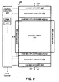
- FIG. 1 illustrates schematically the functional blocks of a non-volatile memory chip.
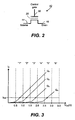
- FIG. 2 illustrates schematically a non-volatile memory cell.
- FIG. 3 illustrates the relation between the source-drain current I D and the control gate voltage V CG for four different charges Q1-Q4 that the floating gate may be selectively storing at any one time.
- FIG. 4 illustrates an example of an NOR array of memory cells.
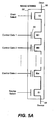
- FIG. 5A illustrates schematically a string of memory cells organized into an NAND string.
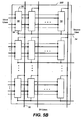
- FIG. 5B illustrates an example of an NAND array of memory cells, constituted from NAND strings such as that shown in FIG. 5A .
- FIG. 6 illustrates schematically, an example of a memory array organized in erasable blocks.
- FIG. 7 illustrates a series of programming voltage pulses in the form of a staircase waveform being applied to a selected word line.
- FIG. 8 illustrates a typical testing setup to determine optimum initial programming voltages for a number of memory chips.
- FIG. 9 illustrates schematically the function blocks of the memory tester testing one of the memory chips shown in FIG. 8 for determination of optimum initial programming voltages.
- FIG. 10 illustrates the function blocks of an alternate memory tester operating with one of the memory chips shown in FIG. 8 for determination of optimum initial programming voltages, according to a preferred embodiment.
- FIG. 11A is a flow diagram illustrating a general scheme for obtaining an estimated starting programming voltage for a given type of word lines in a memory device.
- FIG. 11B illustrates in more detail one embodiment of selecting a good block shown in FIG. 11A .
- FIG. 12 is a flow diagram illustrating a conventional implementation of the steps or determining an initial programming voltage of a page on a word lines
- FIG. 13 is a flow diagram illustrating generally an operation for estimating an optimum starting programming voltage from a sample of word lines within a block
- FIG. 14 is a flow diagram illustrating a specific implementation of the operation shown in FIG. 13 .
- FIG. 15 illustrates the staircase waveform used in the initial programming test of a page of memory cells.
- FIG. 16 is a flow diagram illustrating the determination of starting programming voltage for V PGM trimming, using the staircase waveform scan shown in FIG. 15 .
- FIG. 17 is a flow diagram illustrating a multiple pass determination of starting programming voltage for a sample of pages/word lines.
- FIG. 18 is a flow diagram illustrating the scheme of obtaining a V PGM trimmed value that is weighted toward the faster programming word lines according to an embodiment of the present invention.
- FIG.1 to FIG. 7 illustrate example memory systems in which the various aspects of the present invention may be implemented.
- FIG. 1 illustrates schematically the functional blocks of a non-volatile memory chip.
- the memory chip 100 includes a two-dimensional array of memory cells 200, control circuitry 210, and peripheral circuits such as decoders, read/write circuits and multiplexers.
- the memory array 200 is addressable by word lines (see FIG. 2 ) via row decoders 230A and 230B and by bit lines (see FIG. 2 ) via column decoders 260A and 260B.
- the read/write circuits 270A and 270B allow a page of memory cells to be read or programmed in parallel.
- a page is constituted from a contiguous row of memory cells sharing the same word line.
- block multiplexers 250A and 250B are provided to multiplex the read/write circuits 270A and 270B to the individual pages.
- the control circuitry 210 cooperates with the read/write circuits 270 to perform memory operations on the memory array 200.
- the control circuitry 210 typically includes a state machine 212 and other circuits such as an on-chip address decoder and a power control module (not shown explicitly).
- the state machine 212 provides chip level control of memory operations.
- the memory array 200 is typically organized as a two-dimensional array of memory cells arranged in rows and columns and addressable by word lines and bit lines.
- the array can be formed according to an NOR type or an NAND type architecture.
- FIG. 2 illustrates schematically a non-volatile memory cell.
- the memory cell 10 can be implemented by a field-effect transistor having a charge storage unit 20, such as a floating gate or a dielectric layer.
- the memory cell 10 also includes a source 14, a drain 16, and a control gate 30.
- non-volatile solid-state memory devices There are many commercially successful non-volatile solid-state memory devices being used today. These memory devices may employ different types of memory cells, each type having one or more charge storage element.
- Typical non-volatile memory cells include EEPROM and flash EEPROM. Examples of EEPROM cells and methods of manufacturing them are given in United States patent no. 5,595,924 . Examples of flash EEPROM cells, their uses in memory systems and methods of manufacturing them are given in United States patents nos. 5,070,032 , 5,095,344 , 5,315,541 , 5,343,063 , 5,661,053 , 5,313,421 and 6,222,762 . In particular, examples of memory devices with NAND cell structures are described in United States patent nos. 5,570,315 , 5,903,495 , 6,046,935 .
- the memory state of a cell is usually read by sensing the conduction current across the source and drain electrodes of the cell when a reference voltage is applied to the control gate.
- a corresponding conduction current with respect to a fixed reference control gate voltage may be detected.
- the range of charge programmable onto the floating gate defines a corresponding threshold voltage window or a corresponding conduction current window.
- the threshold voltage for a given memory state under test is set at the control gate and detect if the conduction current is lower or higher than a threshold current.
- the detection of the conduction current relative to a threshold current is accomplished by examining the rate the conduction current is discharging through the capacitance of the bit line.
- FIG. 3 illustrates the relation between the source-drain current I D and the control gate voltage V CG for four different charges Q1-Q4 that the floating gate may be selectively storing at any one time.
- the four solid I D versus V CG curves represent four possible charge levels that can be programmed on a floating gate of a memory cell, respectively corresponding to four possible memory states.
- the threshold voltage window of a population of cells may range from 0.5V to 3.5V.
- Six memory states may be demarcated by partitioning the threshold window into five regions in interval of 0.5V each.
- Q4 is in a memory state "5".
- FIG. 4 illustrates an example of an NOR array of memory cells.
- each row of memory cells are connected by their sources 14 and drains 16 in a daisy-chain manner. This design is sometimes referred to as a virtual ground design.
- the cells 10 in a row have their control gates 30 connected to a word line, such as word line 42.
- the cells in a column have their sources and drains respectively connected to selected bit lines, such as bit lines 34 and 36.
- FIG. 5A illustrates schematically a string of memory cells organized into an NAND string.
- a pair of select transistors S1, S2 controls the memory transistors chain's connection to the external via the NAND string's source terminal 54 and drain terminal 56 respectively.
- the source select transistor S1 when the source select transistor S1 is turned on, the source terminal is coupled to a source line (see FIG. 5B ).
- the drain select transistor S2 is turned on, the drain terminal of the NAND string is coupled to a bit line of the memory array.
- Each memory transistor in the chain has a charge storage element 20 to store a given amount of charge so as to represent an intended memory state.
- a control gate of each memory transistor provides control over read and write operations. As will be seen in FIG. 5B , the control gates of corresponding memory transistors of a row of NAND string are all connected to the same word line. Similarly, a control gate of each of the select transistors S1, S2 provides control access to the NAND string via its source terminal 54 and drain terminal 56 respectively. Likewise, the control gates of corresponding select transistors of a row of NAND string are all connected to the same select line.
- FIG. 5B illustrates an example of an NAND array of memory cells, constituted from NAND strings such as that shown in FIG. 5A .
- a bit line such as bit line 36 is coupled to the drain terminal 56 of each NAND string.
- a source line such as source line 34 is couple to the source terminals 54 of each NAND string.
- control gates along a row of cells in a bank of NAND strings are connected to a word line. An entire row of memory cells in a bank of NAND strings can be addressed by appropriate voltages on the word lines and select lines of the bank of NAND string.
- FIG. 6 illustrates schematically, an example of a memory array organized in erasable blocks.
- Programming of charge storage memory devices can only result in adding more charge to its charge storage elements. Therefore, prior to a program operation, existing charge in charge storage element of a memory cell must be removed (or erased).
- a non-volatile memory such as EEPROM is referred to as a "Flash" EEPROM when an entire array of cells, or significant groups of cells of the array, is electrically erased together (i.e., in a flash). Once erased, the group of cells can then be reprogrammed.
- the group of cells erasable together may consist of one or more addressable erase unit.
- the erase unit or block typically stores one or more pages of data, the page being the unit of programming and reading, although more than one page may be programmed or read in a single operation.
- Each page typically stores one or more sectors of data, the size of the sector being defined by the host system.
- An example is a sector of 512 bytes of user data, following a standard established with magnetic disk drives, plus some number of bytes of overhead information about the user data and/or the block in with it is stored.
- individual memory cells in the memory array 200 are accessible by word lines WL 0 -WL y and bit lines BL 0 - BL x .
- the memory is organized into erase blocks, such as erase blocks 0 , 1 , ... m.
- the NAND string 50 contains 16 memory cells, then the first bank of NAND strings in the array will be accessible by WL 0 to WL 15 .
- the erase block 0 is organized to have all the memory cells of the first bank of NAND strings erased together. In another memory architecture, more than one bank of NAND strings may be erased together.
- FIG. 7 illustrates a series of programming voltage pulses in the form of a staircase waveform being applied to a selected word line.
- a cell When a cell is programmed to a given state, it is subject to successive programming voltage pulses, each time attempting to add incremental charge to the floating gate. In between pulses, the cell is read back or verified to determine its source-drain current relative to the breakpoint level. Programming stops when the current state has been verified to reach the desired state.
- the programming pulse train used may have increasing period or amplitude in order to counteract the accumulating electrons programmed into the charge storage unit of the memory cell.
- Programming circuits generally apply a series of programming pulses to a selected word line. In this way, a page of memory cells whose control gates are connected to the word line can be programmed together.
- FIG.8 to FIG. 10 illustrate example memory testing systems in which the various aspects of the present invention may be implemented.
- the initial programming voltage V PGM0 and the step size must be optimally chosen. If the initial programming voltage V PGM0 is chosen too low, it may require an excessive number of programming pulses to reach the target state. On the other hand if V PGM0 is chosen too high, especially in a multi-state memory, the programming may overshoot the target state in the first pulse. Similar considerations apply to the step size from one pulse to the next. Generally, an optimum step size will allow adequate resolution to transverse each partitioned or demarcated region shown in FIG. 3 in a few steps. An optimum initial programming voltage V PGM0 would reach the target state in a few steps. Generally, the step size can be predetermined based on the number of partitions in the threshold window. The optimum V PGM0 is fairly sensitive to manufacturing variations and is traditionally determined by testing at the factory. This is a process known as V PGM0 trimming.
- FIG. 8 illustrates a typical testing setup to determine optimum initial programming voltages for a number of memory chips.
- a memory tester 300 typically connects to a large number of memory chips 100 for parallel testing.
- a dedicated memory tester is setup to test a number of memory chips in parallel.
- One of the tests is to determine optimum initial programming voltages (V PGM0 trimmings.)
- FIG. 9 illustrates schematically the functional blocks of the memory tester testing one of the memory chips shown in FIG. 8 for determination of optimum initial programming voltages.
- the memory tester 300 issues a series of commands to the memory chip 100 for it to perform a number of program operations using different samples of initial programming voltage.
- the non-volatile memory array 200 has a reserved area (“ROMFUSE") 202 for storing system data.
- the memory tester interacts with the on-chip memory controller 210 via a memory interface 310.
- the tester has a processor 302 that executes a test program in RAM 304 that was initially retrieved from ROM 308.
- the test program execution is facilitated by a set of tester registers 306.
- the test program is controlled by a user through inputs from a user interface 312.
- optimum initial programming voltages V PGM0 are determined for various programming variations, such as different type of word lines and pages. These trimmed values are then stored back into the ROMFUSE 202. During normal use of the memory, the data in the ROMFUSE is loaded into the controller registers 350 on power-up so that the controller 210 has ready access to them during memory operations.
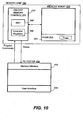
- FIG. 10 illustrate the function blocks of an alternate memory tester operating with one of the memory chips shown in FIG. 8 for determination of optimum initial programming voltages, according to a preferred embodiment.
- the on-chip memory controller 210' is further enhanced with an embedded Built-in Self Test ("BIST") module 340 and additional capacity for a set of controller registers 350.
- BIST Built-in Self Test
- various tests including the V PGM trimming operations described may be performed on-chip.
- an optimum initial programming voltage V PGM0 can be determined either on-chip or by the external tester 330. This determined value is stored back into the ROMFUSE 202.
- the data in the ROMFUSE is loaded into the controller registers 350 on power-up so that the controller 210' has ready access to them during memory operations.
- an external dedicated tester may no longer be required.
- a simple tester 310 implemented by a personal computer, will suffice for operating a large number of memory chips when they are being tested in parallel.
- the memory tester 310 interacts with the on-chip memory controller 210' via a tester memory interface 332. It receives operator inputs from a user interface 334.
- the tester 310 simply instructs each of the memory chips 100 to execute a self test and reports the status at the end of the test for each memory chip.
- the tester 310 gathers the statistics from the test results and makes statistical computations.
- the self-testing on-chip controller 210' has the advantage of doing away with an expensive dedicated tester. Furthermore, it allows the possibility of testing in the field, so that as the memory device ages, its V PGM0 values could be re-trimmed.
- FIG. 11A is a flow diagram illustrating a general scheme for obtaining an estimated starting programming voltage for a given type of word lines in a memory device. As mentioned before, this process is also referred to as programming voltage (“V PGM ”) trimming.
- V PGM programming voltage
- STEP 400 Selecting a Good Block i.
- this step is optional. It may be omitted by simply ignoring any defective word lines encountered.
- a more detailed description of determining a good block is shown in FIG. 11 B.
- group of word lines selected and the type of word lines it seeks to represent share similar programming characteristics.
- STEP 420 Determining an initial programming voltage V PGM0 (i, j) for the page on WL(i, j) such that a staircase pulsing voltage waveform starting from V PGM0 (i, j) will program the whole page to a designated state within a predetermined number of pulses.
- V PGM0 initial programming voltage
- a page of memory cells sharing the word line WL(i, j) is programmed in parallel.
- the staircase waveform increases by a step with every pulse and is budgeted to increase up to the predetermined number of pulses.
- each block may contain three types of word lines having different programming characteristics.
- the first type comprises the first two word lines at the top boundary of the block.
- the second type comprises the last two word lines at the bottom boundary of the block.
- the third type comprises the bulk of the word lines in the core region of the block. To get a better sample for any one of these three types of word lines, a bigger sample is preferably taken, involving more blocks distributed across the memory array.
- different samples of a similar type of word lines may also be formed by taking geometrically similarly located word lines from a set of blocks.
- FIG. 11B illustrates in more detail one embodiment of selecting a good block shown in FIG. 11A .
- a good block is meant to be a block where all its pages of memory cells along the word lines are programmable.
- STEP 400 shown in FIG. 11A is further articulated as follows:
- FIG. 12 is a flow diagram illustrating a conventional implementation of the steps of determining an initial programming voltage of a page on a word line.
- STEP 420 of FIG. 11A the sampled word lines in a block are tested in a piece-meal manner for expediency and efficient use of storage. The next word line will be tested after the test on the previous one has completed. Thus, after the previous word line has been tested to program successfully (or determined to be unprogrammable) will the test be repeated on the next word line.
- STEP 420 shown in FIG. 11A will be further articulated as follows:
- erasing a word line of cells multiple times would entail erasing the rest of the word lines in the same block the same number of times.
- the number of times the block is erased would go up geometrically. As much as half of a memory device's life usage could be used up before it gets to a customer.
- a non-volatile memory having an array of memory cells that are organized into blocks, each block being a block of word lines for accessing memory cells that are erasable together, and each word line containing at least one page of memory cells that are programmable together
- an optimum starting voltage for programming a page of memory cells on a word line in a block is estimated by test programming a sample of similar word lines in the block to obtain a statistical average of individual starting voltages that enable each associated page/word line to be programmable to a designated pattern. This is accomplished by a subjecting all the pages of the sample to a program loop where a series of pulses from a starting programming voltage is applied.
- the page/word line that has been program-verified is removed from further professing and its associated starting programming voltage is saved.
- the block is then erased so that the not yet verified word lines in the sample can be reprogrammed subject to the next program loop the next incremented starting voltage.
- the cycling continues until all word lines in the sample have been program-verified. A statistical average can then be obtained from the individual starting programming voltages to derive an optimum starting programming voltage for the page.
- Testing the sample of word lines in a block by the scheme described has the advantage of reducing the number of block erasures.
- the sample of word line are tested in phase with each other, so that when all the word lines are done programming in each program loop, they are then erased together to be ready for the next program : loop.
- This scheme results in reducing the number of block erasure and can result in a saving of one order of magnitude compared to a conventional scheme.
- the convention scheme shown in FIG. 11 has each word line tested independently with block erasure before every program loop without synchronization with each other. The block erasure associated with every program loop for one word line is then compound for every word line in the sample.
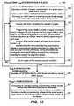
- FIG. 13 is a flow diagram illustrating generally an operation for estimating an optimum starting programming voltage from a sample of word lines within a block.
- the operation is illustrated to have three phases.
- the first phase 500 is for testing and collecting statistics of a sample of pages/word lines within a block. It includes STEP 510 to STEP 550.
- Each word line may support one or more physical page of memory cells.
- each page of memory cells may store one or more logical pages of data depending how many bits each memory cell can store. Thus, multiple logical pages may be associated with a given word line. Insofar as there are any significant variations in programming characteristics in programming the various logical pages, the programming of each logical page may have its own V PGM trimming on the same word line.
- the testing is directed to the programming of a given logical page on a given word line.
- the terminology refers to testing a page or a word line interchangeably.
- the second phase including STEP 560 , is to repeat the first phase 500 on other blocks to be sampled. The first two phases can take place concurrently if the decoding and programming circuits support operating on more than one block.
- the third phase including STEP 570 to STEP 572 , is to compute a statistical average in order to derive an estimated optimum starting Programming voltage for the type of word line under test.
- the present operation essentially cycles through the word lines in the sample by applying a programming step to each word line with an associated starting voltage and then verifying to determine if the page on the word line is programmed to a designated state within a specified program loop target. If any page/word line is program-verified, the starting voltage associated with it is saved. If the page/word line is not yet program-verified, the starting voltage associated with it is incremented. The increment information is also saved, preferably into an accumulator. The cycling through the word lines is repeated on the ones that have not been program-verified so that after a block erasure, they are subject to another programming step with associated incremented starting voltages. This process continues until all the word lines in the sample have been program-verified within the specified program loop target.
- the specified program loop target is a limit for the maximum number of increments allowed. This limit has two different implications when implemented in two different manners.
- the limit sets a relatively low increment ceiling. It sets the maximum number of programming pulses or increments from the given starting voltage before programming of the page is deemed unsuccessful or insufficient. This number is set to be similar to the number of programming steps budgeted during an actual program operation in a normal use of the memory device. For example, in a normal program operation by the user, the programming for a particular logical page is required to be completed within eight to ten programming pulses. In this way, the V PGM trimming test closely duplicates real programming conditions. In general this limit ranges from five to fifteen.
- the programming voltage is allowed to increment until a final voltage results in a programmed page.
- the final voltage is then used to estimate an optimum starting voltage by scaling back a predetermined number of steps.
- the increment of the starting programming voltage is not boundless in case a defective word line is encountered.
- the limit is set to a relative high (e.g., thirty to fifty) number to limit the increments to a maximum predetermined value in case a defective word line is encountered.
- the word line is deemed defective and its V PGM data will be excluded from the statistics.
- the whole block containing the defective word line may be excluded.
- the two embodiments described impose a limit on the program loop for different reasons.
- the first with a lower limit measures programming success from a starting voltage by providing a margin of a number of pulsing steps as in a normal program operation. Programming is deemed successful if completed within the limit. Conversely, unsuccessful programming implies that the starting voltage is set too low.
- the second embodiment with the limit set to a high ceiling is to prevent boundless increments in case a defective word line can never by programmed. Thus, when this limit is reached, it does not mean the starting voltage is too low, but the word line is simply defective.
- a lower limit is also contemplated. If the program loop is completed within the first few (e.g., one or two) steps of the staircase waveform, it will mean that the page has a very fast programming characteristics, which is not typical. Thus, in the case when a page is program-verified within a predetermined lower limit, it is deemed atypical and will also be excluded from the averaging so as not to skew the statistics.
- FIG. 14 is a flow diagram illustrating a specific implementation of the operation shown in FIG. 13 .
- the initial value of a starting programming voltage can be estimated by an initial programming test run of the page on a word line.
- a selected page on a word line is successively programmed by a series of voltage pulses of a staircase waveform with verifications in between the pulses until the page is verified to have been programmed to a designated pattern.
- the final programming voltage at the time the page is program-verified will be used to estimate a starting programming voltage by scaling back a predetermined amount.
- An average starting programming voltage is obtained by considering a sample of similar page/word lines. Any unprogrammable page/word lines in the sample can be ignored so as not to skew the statistics with atypical entries.
- the process is further refined in which the estimated starting programming voltage from a first pass is used as the initial value of the staircase waveform in a second pass.
- the starting programming voltage for a representative page can be estimated.
- the starting programming voltage is estimated by offsetting the final programming voltage negatively by a predetermined number of steps of the staircase waveform.
- the predetermined number of steps is preferably similar to the number of steps budgeted for program success in a normal program operation.
- One advantage of this scaling scheme is that a simple one- or two-pass programming test on each page/word line is sufficient to yield an estimate for the starting programming voltage for the page.
- Each page can be tested independently and does not involve multiple erase operation during the test. Therefore there is no need for management of block erase among a sample of word lines.
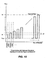
- FIG. 15 illustrates the staircase waveform used in the initial programming test of a page of memory cells.
- the staircase waveform voltage is applied to the word line supporting the page of memory cells.
- a voltage pulse at Vi is applied to perform an incremental programming. This is followed by the voltage changing to VVER suitable for reading the page to verify if the page has been programmed to a designated pattern.
- FIG. 16 is a flow diagram illustrating the determination of starting programming voltage for a given page, using the staircase waveform scan shown in FIG. 15 .
- the estimated starting programming voltage is further refined in a second pass test run where it is used as the initial value of the staircase waveform. In this way, the initial value more closely emulates normal programming operations as compared to the one used in the first pass test run.
- a sample of word lines of similar type are tested to obtain a statistically average starting programming voltage for the type.
- a statistical average is preferably performed after each test run.
- FIG. 17 is a flow diagram illustrating a multiple pass determination of starting programming voltage for a sample of pages/word lines.
- only one pass (STEP 850 to STEP 860) is sufficient to obtain an acceptable estimation of the starting programming voltage.
- a second pass STEP 870 to STEP 880 ) is optionally used to refine the result obtained from the first pass.
- the estimated starting voltage ⁇ V PGM0 > 1 or ⁇ V PGM0 > 2 may be used as input for the initial value for the VPGM trimming scheme described in FIG. 13 and FIG. 14 .
- the tests described in STEP 520 of FIG. 13 and STEP 610 of FIG. 14 require an initial value V PGM0_ 0 for the starting programming voltage. If this value is set too low, the test will have to cycle through more steps before the word line is program-verified. This will be inefficient and consuming more erase cycles of the memory device. On the other hand if the value is set too high, the word line may be over-programmed.
- a scheme for obtaining an optimum starting programming voltage of a representative page of the group includes: forming samples over a set of blocks with one or more word line from a geometrically similar location of each block of the set, obtaining a statistic estimation of a programming voltage from each sample of the set, and selecting a minimum estimation among the set to derive the optimum starting programming voltage.
- the optimum value is weighted towards the faster programming word lines for that group since they require a lower programming voltage compared to the slower ones.
- the programming voltage trimming schemes described in other sections examine a page at a time as to whether all bits in the page are program-verified or not. This implies the test results are catering to the slower programming bits, as these slower bits must also be program-verified before the whole page is deemed program-verified. The consequence is that the starting voltage may be over estimated for the faster programming bits with the danger of over-programming.
- the present sampling and statistical computational scheme allows a lowest value to be selected for the set of starting voltages that was derived from a scheme biased towards the slower programming bits.
- WL2 to WL13 form a group of word lines in the core region of an erase block with somewhat similar but not identical type of programming characteristics.
- a set of blocks is for example, from block0 to block127.
- the samples are formed by selecting a word line from a geometrically similar location of each block of the set.
- a first sample would be constituted from WL2 from block0, WL18 from block 1, WL34 from block2, ..., WL1034 from block127.
- a second sample would be constituted from WL3 from block0, WL19 from block1, WL35 from block2, ..., WL1035 from block127. All in all there will be a set of 128 samples. V PGM trimming operations can be performed on each of the samples and therefore 128 statistical results (e.g. ⁇ V PGM0 > will be obtained. The present method calls for selecting a smallest one among the 128 ⁇ V PGM0 >s.
- FIG. 18 is a flow diagram illustrating the scheme of obtaining a V PGM trimmed value that is weighted toward the faster programming word lines.
- STEP 910 Determining the starting programming voltage for the page by selecting a minimum statistical estimation among the set.
- the scheme of testing individual samples formed by selecting at least a similar page from each block also has the advantage of minimum storage requirement. After each sample is tested, a test result in the form of an average is obtained and stored. Then the next sample is tested in similar manner and its average is then compared to the first one in storage. Whichever average is the lower one will be retained in storage so that only one data need be stored as the set of samples is processed a sample at a time.
- sample average is not as sensitive to the presence of any bad blocks where a large portion of the word lines in it may be defective.
Landscapes
- Engineering & Computer Science (AREA)
- Microelectronics & Electronic Packaging (AREA)
- Computer Hardware Design (AREA)
- Read Only Memory (AREA)
Claims (2)
- Verfahren zum Bestimmen einer optimalen Ausgangsprogrammierspannung (<VpGM0>s) für eine bestimmte Seite von Speicherzellen in einem nichtflüchtigen Speicher mit einem Array (200) von Speicherzellen, das in löschbare Blöcke organisiert ist, wobei jeder löschbare Block einen Wortzeilenblock zum Zugreifen auf Speicherzellen enthält, die gemeinsam löschbar sind, und wobei jede Wortzeile zumindest eine Seite vorn Speicherzellen enthält, die gemeinsam programmierbar sind, wobei das Verfahren umfasst:Auswählen einer Gruppe von Seiten, die für die bestimmte Seite innerhalb eines Blocks repräsentativ ist;Auswählen eines Blocksatzes; Bilden eines Probensatzes durch Auswählen zumindest eines Seite aus jedem Block des Blocksatzes, wobei die Seite an einem geometrisch ähnlichen Ort jedes Blockes im Blocksatz positioniert ist;Bereitstellen einer Programmierspannung zum Programmieren jeder Seite jeder Probe des Probensatzes, wobei die Programmierspannung eine Treppenwellenform mit einem Ausgangswert aufweist;Löschen der Seiten des Probensatzes;für jede Seite in jeder Probe des Probensatzes Programmieren und Verifizieren der Seite Stufe für Stufe der Treppenwellenform, bis entweder eine maximale Anzahl von Programmierimpulsen erreicht wurde oder die Seite auf ein Zielnnuster programmiert wurde;wenn die Seite auf das Zielmuster programmiert wurde, wird eine Endprogrammierspannung als Teil einer gesammelten Statistik akkumuliert, wobei die gesammelte Statistik akkumulierte Anfangsprogrammierspannungen enthält, die mit programmierbaren Seiten aus der Probe assoziiert sind;Berechnen einer durchschnittlichen Anfangsprogrammierspannung (<VPGM0>) für jede Probe des Probensatzes aus der gesammelten Statistik;wobei der Schritt des Bestimmens einer optimalen Ausgangsprogrammierspannung für die bestimmte Seite durch Auswählen der durchschnittlichen Mindestanfangsprogrammierspannung aus dem Probensatz erfolgt.
- Nichtflüchtiger Speicher, umfassend:ein Array (200) von Speicherzellen, das in löschbare Blöcke organisiert ist, wobei jeder löschbare Block einen Wortzeilenblock zum Zugreifen auf Speicherzellen enthält, die gemeinsam löschbar sind, und wobei jede Wortzeile zumindest eine Seite von Speicherzellen enthält, die gemeinsam programmierbar sind;eine designierte Gruppe von Seiten, die für die bestimmte Seite innerhalb eines Blocks repräsentativ ist;einen Blocksatz;einen Probensatz, der durch Auswählen zumindest einer Seite aus jedem Block des Blocksatzes gebildet wird, wobei die Seite an einem geometrisch ähnlichen Ort jedes Blocks im Blocksatz positioniert ist;eine assoziierte Programmierspannung zum Programmieren jeder Seite jeder Probe des Probensatzes, wobei die assoziierte Programmierspannung eine Treppenwellenform mit einem Ausgangswert aufweist;ein integriertes Selbsttestmodul zum Bestimmen einer optimalen Ausgangsprogrammierspannung (<VPGM0>s) für eine bestimmte Seite, wobei das Modul angeordnet ist, um Speicheroperationen bereitzustellen, enthaltend:(a) Löschen der Seiten des Probensatzes;(b) für jede Seite in jeder Probe Programmieren und Verifizieren der Seite Stufe für Stufe der Treppenwellenform, bis entweder eine maximale Anzahl von Programmierimpulsen erreicht wurde oder die Seite auf ein Zielmuster programmiert wurde;wenn die Seite auf das Zielmuster programmiert wurde, Akkumulieren einer Endprogrammierspannung als Teil einer gesammelten Statistik;Bereitstellen der gesammelten Statistik zum Berechnen einer durchschnittlichen Anfangsprogrammierspannung (<VPGM0>) für jede Probe des Probensatzes;wobei die gesammelte Statistik akkumulierte Anfangsprogrammierspannungen enthält, die mit programmierbaren Seiten aus dem Probensatz assoziiert sind;Bestimmen der optimalen Ausgangsprogrammierspannung für die bestimmte Seite durch Auswählen der durchschnittlichen Mindestanfangsprogrammierspannung aus dem Probensatz.
Priority Applications (1)
| Application Number | Priority Date | Filing Date | Title |
|---|---|---|---|
| EP11175624A EP2383748A3 (de) | 2006-09-12 | 2007-08-31 | Nichtflüchtiger Speicher und Verfahren zur linearen Schätzung von anfänglichen Programmierungsspannung |
Applications Claiming Priority (3)
| Application Number | Priority Date | Filing Date | Title |
|---|---|---|---|
| US11/531,230 US7599223B2 (en) | 2006-09-12 | 2006-09-12 | Non-volatile memory with linear estimation of initial programming voltage |
| US11/531,227 US7453731B2 (en) | 2006-09-12 | 2006-09-12 | Method for non-volatile memory with linear estimation of initial programming voltage |
| PCT/US2007/077449 WO2008033693A2 (en) | 2006-09-12 | 2007-08-31 | Non-volatile memory and method for linear estimation of initial programming voltage |
Related Child Applications (1)
| Application Number | Title | Priority Date | Filing Date |
|---|---|---|---|
| EP11175624.3 Division-Into | 2011-07-27 |
Publications (2)
| Publication Number | Publication Date |
|---|---|
| EP2074626A2 EP2074626A2 (de) | 2009-07-01 |
| EP2074626B1 true EP2074626B1 (de) | 2012-11-28 |
Family
ID=39185663
Family Applications (2)
| Application Number | Title | Priority Date | Filing Date |
|---|---|---|---|
| EP11175624A Withdrawn EP2383748A3 (de) | 2006-09-12 | 2007-08-31 | Nichtflüchtiger Speicher und Verfahren zur linearen Schätzung von anfänglichen Programmierungsspannung |
| EP07841761A Not-in-force EP2074626B1 (de) | 2006-09-12 | 2007-08-31 | Nichtflüchtiger speicher und verfahren für lineare schätzung der eingangsprogrammierungsspannung |
Family Applications Before (1)
| Application Number | Title | Priority Date | Filing Date |
|---|---|---|---|
| EP11175624A Withdrawn EP2383748A3 (de) | 2006-09-12 | 2007-08-31 | Nichtflüchtiger Speicher und Verfahren zur linearen Schätzung von anfänglichen Programmierungsspannung |
Country Status (5)
| Country | Link |
|---|---|
| EP (2) | EP2383748A3 (de) |
| JP (1) | JP4819951B2 (de) |
| KR (1) | KR101410288B1 (de) |
| TW (1) | TWI457929B (de) |
| WO (1) | WO2008033693A2 (de) |
Families Citing this family (11)
| Publication number | Priority date | Publication date | Assignee | Title |
|---|---|---|---|---|
| US7453731B2 (en) | 2006-09-12 | 2008-11-18 | Sandisk Corporation | Method for non-volatile memory with linear estimation of initial programming voltage |
| US7606077B2 (en) | 2006-09-12 | 2009-10-20 | Sandisk Corporation | Non-volatile memory with reduced erase/write cycling during trimming of initial programming voltage |
| US7599223B2 (en) | 2006-09-12 | 2009-10-06 | Sandisk Corporation | Non-volatile memory with linear estimation of initial programming voltage |
| US7606091B2 (en) | 2006-09-12 | 2009-10-20 | Sandisk Corporation | Method for non-volatile memory with reduced erase/write cycling during trimming of initial programming voltage |
| JP5032290B2 (ja) * | 2007-12-14 | 2012-09-26 | 株式会社東芝 | 不揮発性半導体記憶装置 |
| KR100960479B1 (ko) * | 2007-12-24 | 2010-06-01 | 주식회사 하이닉스반도체 | 플래시 메모리 장치 및 동작 방법 |
| KR100996108B1 (ko) * | 2009-01-21 | 2010-11-22 | 주식회사 하이닉스반도체 | 불휘발성 메모리 장치의 프로그램 방법 |
| KR101616099B1 (ko) | 2009-12-03 | 2016-04-27 | 삼성전자주식회사 | 플래시 메모리 장치 및 그것의 프로그램 방법 |
| KR20190000663A (ko) * | 2017-06-23 | 2019-01-03 | 에스케이하이닉스 주식회사 | 메모리 장치 및 그 동작 방법 |
| US10818358B2 (en) | 2017-09-22 | 2020-10-27 | Toshiba Memory Corporation | Memory system including a semiconductor memory having a memory cell and a write circuit configured to write data to the memory cell |
| JP2020119618A (ja) | 2019-01-21 | 2020-08-06 | キオクシア株式会社 | メモリシステム |
Family Cites Families (30)
| Publication number | Priority date | Publication date | Assignee | Title |
|---|---|---|---|---|
| US5095344A (en) | 1988-06-08 | 1992-03-10 | Eliyahou Harari | Highly compact eprom and flash eeprom devices |
| US5070032A (en) | 1989-03-15 | 1991-12-03 | Sundisk Corporation | Method of making dense flash eeprom semiconductor memory structures |
| US5172338B1 (en) | 1989-04-13 | 1997-07-08 | Sandisk Corp | Multi-state eeprom read and write circuits and techniques |
| US5343063A (en) | 1990-12-18 | 1994-08-30 | Sundisk Corporation | Dense vertical programmable read only memory cell structure and processes for making them |
| US6222762B1 (en) | 1992-01-14 | 2001-04-24 | Sandisk Corporation | Multi-state memory |
| US5313421A (en) | 1992-01-14 | 1994-05-17 | Sundisk Corporation | EEPROM with split gate source side injection |
| TW231343B (de) * | 1992-03-17 | 1994-10-01 | Hitachi Seisakusyo Kk | |
| JPH0625083A (ja) * | 1992-07-10 | 1994-02-01 | Daicel Chem Ind Ltd | エステル又はラクトンの製造方法 |
| US5315541A (en) | 1992-07-24 | 1994-05-24 | Sundisk Corporation | Segmented column memory array |
| US5555204A (en) | 1993-06-29 | 1996-09-10 | Kabushiki Kaisha Toshiba | Non-volatile semiconductor memory device |
| KR0169267B1 (ko) | 1993-09-21 | 1999-02-01 | 사토 후미오 | 불휘발성 반도체 기억장치 |
| US5661053A (en) | 1994-05-25 | 1997-08-26 | Sandisk Corporation | Method of making dense flash EEPROM cell array and peripheral supporting circuits formed in deposited field oxide with the use of spacers |
| KR0185611B1 (ko) * | 1995-12-11 | 1999-04-15 | 김광호 | 불휘발성 반도체 메모리장치의 고전압 레벨 최적화 회로 및 그 방법 |
| US5903495A (en) | 1996-03-18 | 1999-05-11 | Kabushiki Kaisha Toshiba | Semiconductor device and memory system |
| US5768192A (en) | 1996-07-23 | 1998-06-16 | Saifun Semiconductors, Ltd. | Non-volatile semiconductor memory cell utilizing asymmetrical charge trapping |
| US6768165B1 (en) | 1997-08-01 | 2004-07-27 | Saifun Semiconductors Ltd. | Two bit non-volatile electrically erasable and programmable semiconductor memory cell utilizing asymmetrical charge trapping |
| JPH11134879A (ja) * | 1997-10-30 | 1999-05-21 | Toshiba Corp | 不揮発性半導体記憶装置 |
| US6205055B1 (en) * | 2000-02-25 | 2001-03-20 | Advanced Micro Devices, Inc. | Dynamic memory cell programming voltage |
| US6304487B1 (en) * | 2000-02-28 | 2001-10-16 | Advanced Micro Devices, Inc. | Register driven means to control programming voltages |
| US6246611B1 (en) * | 2000-02-28 | 2001-06-12 | Advanced Micro Devices, Inc. | System for erasing a memory cell |
| US6928001B2 (en) * | 2000-12-07 | 2005-08-09 | Saifun Semiconductors Ltd. | Programming and erasing methods for a non-volatile memory cell |
| JP3866627B2 (ja) * | 2002-07-12 | 2007-01-10 | 株式会社東芝 | 不揮発性半導体メモリ |
| KR100541819B1 (ko) * | 2003-12-30 | 2006-01-10 | 삼성전자주식회사 | 스타트 프로그램 전압을 차등적으로 사용하는 불휘발성반도체 메모리 장치 및 그에 따른 프로그램 방법 |
| TWI267864B (en) * | 2004-05-06 | 2006-12-01 | Samsung Electronics Co Ltd | Method and device for programming control information |
| US7251158B2 (en) * | 2004-06-10 | 2007-07-31 | Spansion Llc | Erase algorithm for multi-level bit flash memory |
| US7092290B2 (en) * | 2004-11-16 | 2006-08-15 | Sandisk Corporation | High speed programming system with reduced over programming |
| JP4909670B2 (ja) * | 2006-01-24 | 2012-04-04 | 株式会社東芝 | 不揮発性半導体記憶装置及びそれを用いた不揮発性メモリシステム |
| WO2008033679A2 (en) * | 2006-09-12 | 2008-03-20 | Sandisk Corporation | Non-volatile memory and method for reduced erase/write cycling during trimming of initial programming voltage |
| KR100780773B1 (ko) * | 2006-11-03 | 2007-11-30 | 주식회사 하이닉스반도체 | 플래시 메모리소자의 프로그램 시작 바이어스 설정방법 및이를 이용한 프로그램 방법 |
| JP2008262623A (ja) * | 2007-04-11 | 2008-10-30 | Toshiba Corp | 不揮発性半導体記憶装置 |
-
2007
- 2007-08-31 JP JP2009528389A patent/JP4819951B2/ja not_active Expired - Fee Related
- 2007-08-31 EP EP11175624A patent/EP2383748A3/de not_active Withdrawn
- 2007-08-31 WO PCT/US2007/077449 patent/WO2008033693A2/en active Application Filing
- 2007-08-31 EP EP07841761A patent/EP2074626B1/de not_active Not-in-force
- 2007-08-31 KR KR1020097005158A patent/KR101410288B1/ko active IP Right Grant
- 2007-09-12 TW TW096134052A patent/TWI457929B/zh not_active IP Right Cessation
Also Published As
| Publication number | Publication date |
|---|---|
| JP2010503946A (ja) | 2010-02-04 |
| EP2383748A2 (de) | 2011-11-02 |
| WO2008033693A2 (en) | 2008-03-20 |
| KR101410288B1 (ko) | 2014-06-20 |
| JP4819951B2 (ja) | 2011-11-24 |
| KR20090074735A (ko) | 2009-07-07 |
| TW200837755A (en) | 2008-09-16 |
| EP2383748A3 (de) | 2012-03-28 |
| WO2008033693A3 (en) | 2008-08-07 |
| EP2074626A2 (de) | 2009-07-01 |
| TWI457929B (zh) | 2014-10-21 |
Similar Documents
| Publication | Publication Date | Title |
|---|---|---|
| US7599223B2 (en) | Non-volatile memory with linear estimation of initial programming voltage | |
| US7453731B2 (en) | Method for non-volatile memory with linear estimation of initial programming voltage | |
| US7606091B2 (en) | Method for non-volatile memory with reduced erase/write cycling during trimming of initial programming voltage | |
| EP2062265B1 (de) | Nichtflüchtiger speicher und verfahren für reduzierten lösch-/schreibzyklus während des abgleichs von eiingangsprogrammierungsspannung | |
| EP2074626B1 (de) | Nichtflüchtiger speicher und verfahren für lineare schätzung der eingangsprogrammierungsspannung | |
| US7606077B2 (en) | Non-volatile memory with reduced erase/write cycling during trimming of initial programming voltage | |
| EP1894206B1 (de) | Speicherblocklöschung in einer flash-speicher-vorrichtung | |
| US7965562B2 (en) | Predictive programming in non-volatile memory | |
| US8971121B2 (en) | Method and devices for memory cell erasure with a programming monitor of reference cells | |
| WO2008124760A2 (en) | Non-volatile memory and method for predictive programming | |
| US20080253193A1 (en) | Non-Volatile Memory with Predictive Programming | |
| US9442842B2 (en) | Memory system performance configuration | |
| Martirosyan et al. | An efficient testing methodology for embedded flash memories |
Legal Events
| Date | Code | Title | Description |
|---|---|---|---|
| PUAI | Public reference made under article 153(3) epc to a published international application that has entered the european phase |
Free format text: ORIGINAL CODE: 0009012 |
|
| 17P | Request for examination filed |
Effective date: 20090218 |
|
| AK | Designated contracting states |
Kind code of ref document: A2 Designated state(s): AT BE BG CH CY CZ DE DK EE ES FI FR GB GR HU IE IS IT LI LT LU LV MC MT NL PL PT RO SE SI SK TR |
|
| AX | Request for extension of the european patent |
Extension state: AL BA HR MK RS |
|
| 17Q | First examination report despatched |
Effective date: 20090818 |
|
| DAX | Request for extension of the european patent (deleted) | ||
| GRAP | Despatch of communication of intention to grant a patent |
Free format text: ORIGINAL CODE: EPIDOSNIGR1 |
|
| RAP1 | Party data changed (applicant data changed or rights of an application transferred) |
Owner name: SANDISK TECHNOLOGIES INC. |
|
| GRAS | Grant fee paid |
Free format text: ORIGINAL CODE: EPIDOSNIGR3 |
|
| RIN1 | Information on inventor provided before grant (corrected) |
Inventor name: LI, YAN Inventor name: TU, LOC Inventor name: HOOK, CHARLES MOANA |
|
| GRAA | (expected) grant |
Free format text: ORIGINAL CODE: 0009210 |
|
| AK | Designated contracting states |
Kind code of ref document: B1 Designated state(s): AT BE BG CH CY CZ DE DK EE ES FI FR GB GR HU IE IS IT LI LT LU LV MC MT NL PL PT RO SE SI SK TR |
|
| REG | Reference to a national code |
Ref country code: GB Ref legal event code: FG4D |
|
| REG | Reference to a national code |
Ref country code: CH Ref legal event code: EP |
|
| REG | Reference to a national code |
Ref country code: AT Ref legal event code: REF Ref document number: 586538 Country of ref document: AT Kind code of ref document: T Effective date: 20121215 |
|
| REG | Reference to a national code |
Ref country code: IE Ref legal event code: FG4D |
|
| REG | Reference to a national code |
Ref country code: DE Ref legal event code: R096 Ref document number: 602007027038 Country of ref document: DE Effective date: 20130117 |
|
| REG | Reference to a national code |
Ref country code: NL Ref legal event code: T3 |
|
| REG | Reference to a national code |
Ref country code: AT Ref legal event code: MK05 Ref document number: 586538 Country of ref document: AT Kind code of ref document: T Effective date: 20121128 |
|
| REG | Reference to a national code |
Ref country code: LT Ref legal event code: MG4D |
|
| PG25 | Lapsed in a contracting state [announced via postgrant information from national office to epo] |
Ref country code: FI Free format text: LAPSE BECAUSE OF FAILURE TO SUBMIT A TRANSLATION OF THE DESCRIPTION OR TO PAY THE FEE WITHIN THE PRESCRIBED TIME-LIMIT Effective date: 20121128 Ref country code: ES Free format text: LAPSE BECAUSE OF FAILURE TO SUBMIT A TRANSLATION OF THE DESCRIPTION OR TO PAY THE FEE WITHIN THE PRESCRIBED TIME-LIMIT Effective date: 20130311 Ref country code: LT Free format text: LAPSE BECAUSE OF FAILURE TO SUBMIT A TRANSLATION OF THE DESCRIPTION OR TO PAY THE FEE WITHIN THE PRESCRIBED TIME-LIMIT Effective date: 20121128 Ref country code: SE Free format text: LAPSE BECAUSE OF FAILURE TO SUBMIT A TRANSLATION OF THE DESCRIPTION OR TO PAY THE FEE WITHIN THE PRESCRIBED TIME-LIMIT Effective date: 20121128 |
|
| PG25 | Lapsed in a contracting state [announced via postgrant information from national office to epo] |
Ref country code: SI Free format text: LAPSE BECAUSE OF FAILURE TO SUBMIT A TRANSLATION OF THE DESCRIPTION OR TO PAY THE FEE WITHIN THE PRESCRIBED TIME-LIMIT Effective date: 20121128 Ref country code: BE Free format text: LAPSE BECAUSE OF FAILURE TO SUBMIT A TRANSLATION OF THE DESCRIPTION OR TO PAY THE FEE WITHIN THE PRESCRIBED TIME-LIMIT Effective date: 20121128 Ref country code: LV Free format text: LAPSE BECAUSE OF FAILURE TO SUBMIT A TRANSLATION OF THE DESCRIPTION OR TO PAY THE FEE WITHIN THE PRESCRIBED TIME-LIMIT Effective date: 20121128 Ref country code: GR Free format text: LAPSE BECAUSE OF FAILURE TO SUBMIT A TRANSLATION OF THE DESCRIPTION OR TO PAY THE FEE WITHIN THE PRESCRIBED TIME-LIMIT Effective date: 20130301 Ref country code: PL Free format text: LAPSE BECAUSE OF FAILURE TO SUBMIT A TRANSLATION OF THE DESCRIPTION OR TO PAY THE FEE WITHIN THE PRESCRIBED TIME-LIMIT Effective date: 20121128 Ref country code: PT Free format text: LAPSE BECAUSE OF FAILURE TO SUBMIT A TRANSLATION OF THE DESCRIPTION OR TO PAY THE FEE WITHIN THE PRESCRIBED TIME-LIMIT Effective date: 20130328 |
|
| PG25 | Lapsed in a contracting state [announced via postgrant information from national office to epo] |
Ref country code: AT Free format text: LAPSE BECAUSE OF FAILURE TO SUBMIT A TRANSLATION OF THE DESCRIPTION OR TO PAY THE FEE WITHIN THE PRESCRIBED TIME-LIMIT Effective date: 20121128 |
|
| PG25 | Lapsed in a contracting state [announced via postgrant information from national office to epo] |
Ref country code: SK Free format text: LAPSE BECAUSE OF FAILURE TO SUBMIT A TRANSLATION OF THE DESCRIPTION OR TO PAY THE FEE WITHIN THE PRESCRIBED TIME-LIMIT Effective date: 20121128 Ref country code: CZ Free format text: LAPSE BECAUSE OF FAILURE TO SUBMIT A TRANSLATION OF THE DESCRIPTION OR TO PAY THE FEE WITHIN THE PRESCRIBED TIME-LIMIT Effective date: 20121128 Ref country code: DK Free format text: LAPSE BECAUSE OF FAILURE TO SUBMIT A TRANSLATION OF THE DESCRIPTION OR TO PAY THE FEE WITHIN THE PRESCRIBED TIME-LIMIT Effective date: 20121128 Ref country code: EE Free format text: LAPSE BECAUSE OF FAILURE TO SUBMIT A TRANSLATION OF THE DESCRIPTION OR TO PAY THE FEE WITHIN THE PRESCRIBED TIME-LIMIT Effective date: 20121128 Ref country code: BG Free format text: LAPSE BECAUSE OF FAILURE TO SUBMIT A TRANSLATION OF THE DESCRIPTION OR TO PAY THE FEE WITHIN THE PRESCRIBED TIME-LIMIT Effective date: 20130228 |
|
| PG25 | Lapsed in a contracting state [announced via postgrant information from national office to epo] |
Ref country code: RO Free format text: LAPSE BECAUSE OF FAILURE TO SUBMIT A TRANSLATION OF THE DESCRIPTION OR TO PAY THE FEE WITHIN THE PRESCRIBED TIME-LIMIT Effective date: 20121128 Ref country code: IT Free format text: LAPSE BECAUSE OF FAILURE TO SUBMIT A TRANSLATION OF THE DESCRIPTION OR TO PAY THE FEE WITHIN THE PRESCRIBED TIME-LIMIT Effective date: 20121128 |
|
| PLBE | No opposition filed within time limit |
Free format text: ORIGINAL CODE: 0009261 |
|
| STAA | Information on the status of an ep patent application or granted ep patent |
Free format text: STATUS: NO OPPOSITION FILED WITHIN TIME LIMIT |
|
| PGFP | Annual fee paid to national office [announced via postgrant information from national office to epo] |
Ref country code: NL Payment date: 20130810 Year of fee payment: 7 |
|
| 26N | No opposition filed |
Effective date: 20130829 |
|
| PG25 | Lapsed in a contracting state [announced via postgrant information from national office to epo] |
Ref country code: CY Free format text: LAPSE BECAUSE OF FAILURE TO SUBMIT A TRANSLATION OF THE DESCRIPTION OR TO PAY THE FEE WITHIN THE PRESCRIBED TIME-LIMIT Effective date: 20121128 |
|
| PGFP | Annual fee paid to national office [announced via postgrant information from national office to epo] |
Ref country code: FR Payment date: 20130808 Year of fee payment: 7 |
|
| REG | Reference to a national code |
Ref country code: DE Ref legal event code: R097 Ref document number: 602007027038 Country of ref document: DE Effective date: 20130829 |
|
| REG | Reference to a national code |
Ref country code: CH Ref legal event code: PL |
|
| PG25 | Lapsed in a contracting state [announced via postgrant information from national office to epo] |
Ref country code: CH Free format text: LAPSE BECAUSE OF NON-PAYMENT OF DUE FEES Effective date: 20130831 Ref country code: LI Free format text: LAPSE BECAUSE OF NON-PAYMENT OF DUE FEES Effective date: 20130831 Ref country code: MC Free format text: LAPSE BECAUSE OF FAILURE TO SUBMIT A TRANSLATION OF THE DESCRIPTION OR TO PAY THE FEE WITHIN THE PRESCRIBED TIME-LIMIT Effective date: 20121128 |
|
| REG | Reference to a national code |
Ref country code: IE Ref legal event code: MM4A |
|
| PG25 | Lapsed in a contracting state [announced via postgrant information from national office to epo] |
Ref country code: IE Free format text: LAPSE BECAUSE OF NON-PAYMENT OF DUE FEES Effective date: 20130831 |
|
| REG | Reference to a national code |
Ref country code: NL Ref legal event code: V1 Effective date: 20150301 |
|
| PG25 | Lapsed in a contracting state [announced via postgrant information from national office to epo] |
Ref country code: NL Free format text: LAPSE BECAUSE OF NON-PAYMENT OF DUE FEES Effective date: 20150301 |
|
| REG | Reference to a national code |
Ref country code: FR Ref legal event code: ST Effective date: 20150430 |
|
| PG25 | Lapsed in a contracting state [announced via postgrant information from national office to epo] |
Ref country code: MT Free format text: LAPSE BECAUSE OF FAILURE TO SUBMIT A TRANSLATION OF THE DESCRIPTION OR TO PAY THE FEE WITHIN THE PRESCRIBED TIME-LIMIT Effective date: 20121128 Ref country code: TR Free format text: LAPSE BECAUSE OF FAILURE TO SUBMIT A TRANSLATION OF THE DESCRIPTION OR TO PAY THE FEE WITHIN THE PRESCRIBED TIME-LIMIT Effective date: 20121128 |
|
| PG25 | Lapsed in a contracting state [announced via postgrant information from national office to epo] |
Ref country code: HU Free format text: LAPSE BECAUSE OF FAILURE TO SUBMIT A TRANSLATION OF THE DESCRIPTION OR TO PAY THE FEE WITHIN THE PRESCRIBED TIME-LIMIT; INVALID AB INITIO Effective date: 20070831 Ref country code: LU Free format text: LAPSE BECAUSE OF NON-PAYMENT OF DUE FEES Effective date: 20130831 |
|
| PG25 | Lapsed in a contracting state [announced via postgrant information from national office to epo] |
Ref country code: FR Free format text: LAPSE BECAUSE OF NON-PAYMENT OF DUE FEES Effective date: 20140901 |
|
| PG25 | Lapsed in a contracting state [announced via postgrant information from national office to epo] |
Ref country code: IS Free format text: LAPSE BECAUSE OF FAILURE TO SUBMIT A TRANSLATION OF THE DESCRIPTION OR TO PAY THE FEE WITHIN THE PRESCRIBED TIME-LIMIT Effective date: 20121128 |
|
| REG | Reference to a national code |
Ref country code: DE Ref legal event code: R082 Ref document number: 602007027038 Country of ref document: DE Representative=s name: MARKS & CLERK (LUXEMBOURG) LLP, LU Ref country code: DE Ref legal event code: R081 Ref document number: 602007027038 Country of ref document: DE Owner name: SANDISK TECHNOLOGIES LLC, PLANO, US Free format text: FORMER OWNER: SANDISK TECHNOLOGIES INC., PLANO, TEX., US |
|
| PGFP | Annual fee paid to national office [announced via postgrant information from national office to epo] |
Ref country code: DE Payment date: 20180821 Year of fee payment: 12 |
|
| PGFP | Annual fee paid to national office [announced via postgrant information from national office to epo] |
Ref country code: GB Payment date: 20180829 Year of fee payment: 12 |
|
| REG | Reference to a national code |
Ref country code: DE Ref legal event code: R119 Ref document number: 602007027038 Country of ref document: DE |
|
| GBPC | Gb: european patent ceased through non-payment of renewal fee |
Effective date: 20190831 |
|
| PG25 | Lapsed in a contracting state [announced via postgrant information from national office to epo] |
Ref country code: DE Free format text: LAPSE BECAUSE OF NON-PAYMENT OF DUE FEES Effective date: 20200303 |
|
| PG25 | Lapsed in a contracting state [announced via postgrant information from national office to epo] |
Ref country code: GB Free format text: LAPSE BECAUSE OF NON-PAYMENT OF DUE FEES Effective date: 20190831 |