EP2073236B1 - MEMS-Mikroschalter mit leitfähigem Mechanikstopp - Google Patents
MEMS-Mikroschalter mit leitfähigem Mechanikstopp Download PDFInfo
- Publication number
- EP2073236B1 EP2073236B1 EP08171380A EP08171380A EP2073236B1 EP 2073236 B1 EP2073236 B1 EP 2073236B1 EP 08171380 A EP08171380 A EP 08171380A EP 08171380 A EP08171380 A EP 08171380A EP 2073236 B1 EP2073236 B1 EP 2073236B1
- Authority
- EP
- European Patent Office
- Prior art keywords
- substrate
- conductive
- movable actuator
- contact
- movable
- Prior art date
- Legal status (The legal status is an assumption and is not a legal conclusion. Google has not performed a legal analysis and makes no representation as to the accuracy of the status listed.)
- Active
Links
- 239000000758 substrate Substances 0.000 claims description 151
- 238000002955 isolation Methods 0.000 claims description 9
- 239000004020 conductor Substances 0.000 description 6
- 238000000034 method Methods 0.000 description 5
- 239000000463 material Substances 0.000 description 4
- 229910001020 Au alloy Inorganic materials 0.000 description 3
- 229910045601 alloy Inorganic materials 0.000 description 3
- 239000000956 alloy Substances 0.000 description 3
- PCHJSUWPFVWCPO-UHFFFAOYSA-N gold Chemical compound [Au] PCHJSUWPFVWCPO-UHFFFAOYSA-N 0.000 description 3
- 239000010931 gold Substances 0.000 description 3
- 229910052737 gold Inorganic materials 0.000 description 3
- 239000003353 gold alloy Substances 0.000 description 3
- 239000000203 mixture Substances 0.000 description 3
- 230000008859 change Effects 0.000 description 2
- 239000012212 insulator Substances 0.000 description 2
- BASFCYQUMIYNBI-UHFFFAOYSA-N platinum Chemical compound [Pt] BASFCYQUMIYNBI-UHFFFAOYSA-N 0.000 description 2
- 230000008569 process Effects 0.000 description 2
- 229910000838 Al alloy Inorganic materials 0.000 description 1
- 229910001260 Pt alloy Inorganic materials 0.000 description 1
- 229910052581 Si3N4 Inorganic materials 0.000 description 1
- VYPSYNLAJGMNEJ-UHFFFAOYSA-N Silicium dioxide Chemical compound O=[Si]=O VYPSYNLAJGMNEJ-UHFFFAOYSA-N 0.000 description 1
- 238000009825 accumulation Methods 0.000 description 1
- XAGFODPZIPBFFR-UHFFFAOYSA-N aluminium Chemical compound [Al] XAGFODPZIPBFFR-UHFFFAOYSA-N 0.000 description 1
- QRJOYPHTNNOAOJ-UHFFFAOYSA-N copper gold Chemical compound [Cu].[Au] QRJOYPHTNNOAOJ-UHFFFAOYSA-N 0.000 description 1
- 230000008878 coupling Effects 0.000 description 1
- 238000010168 coupling process Methods 0.000 description 1
- 238000005859 coupling reaction Methods 0.000 description 1
- 230000001419 dependent effect Effects 0.000 description 1
- 238000005516 engineering process Methods 0.000 description 1
- 229910052732 germanium Inorganic materials 0.000 description 1
- GNPVGFCGXDBREM-UHFFFAOYSA-N germanium atom Chemical compound [Ge] GNPVGFCGXDBREM-UHFFFAOYSA-N 0.000 description 1
- 238000009413 insulation Methods 0.000 description 1
- 230000007257 malfunction Effects 0.000 description 1
- 229910001092 metal group alloy Inorganic materials 0.000 description 1
- TWNQGVIAIRXVLR-UHFFFAOYSA-N oxo(oxoalumanyloxy)alumane Chemical compound O=[Al]O[Al]=O TWNQGVIAIRXVLR-UHFFFAOYSA-N 0.000 description 1
- 230000004044 response Effects 0.000 description 1
- 229910052710 silicon Inorganic materials 0.000 description 1
- 239000010703 silicon Substances 0.000 description 1
- HQVNEWCFYHHQES-UHFFFAOYSA-N silicon nitride Chemical compound N12[Si]34N5[Si]62N3[Si]51N64 HQVNEWCFYHHQES-UHFFFAOYSA-N 0.000 description 1
- 229910052814 silicon oxide Inorganic materials 0.000 description 1
Images
Classifications
-
- H—ELECTRICITY
- H01—ELECTRIC ELEMENTS
- H01H—ELECTRIC SWITCHES; RELAYS; SELECTORS; EMERGENCY PROTECTIVE DEVICES
- H01H59/00—Electrostatic relays; Electro-adhesion relays
- H01H59/0009—Electrostatic relays; Electro-adhesion relays making use of micromechanics
-
- B—PERFORMING OPERATIONS; TRANSPORTING
- B81—MICROSTRUCTURAL TECHNOLOGY
- B81B—MICROSTRUCTURAL DEVICES OR SYSTEMS, e.g. MICROMECHANICAL DEVICES
- B81B7/00—Microstructural systems; Auxiliary parts of microstructural devices or systems
- B81B7/02—Microstructural systems; Auxiliary parts of microstructural devices or systems containing distinct electrical or optical devices of particular relevance for their function, e.g. microelectro-mechanical systems [MEMS]
-
- B—PERFORMING OPERATIONS; TRANSPORTING
- B81—MICROSTRUCTURAL TECHNOLOGY
- B81B—MICROSTRUCTURAL DEVICES OR SYSTEMS, e.g. MICROMECHANICAL DEVICES
- B81B7/00—Microstructural systems; Auxiliary parts of microstructural devices or systems
-
- H—ELECTRICITY
- H01—ELECTRIC ELEMENTS
- H01H—ELECTRIC SWITCHES; RELAYS; SELECTORS; EMERGENCY PROTECTIVE DEVICES
- H01H59/00—Electrostatic relays; Electro-adhesion relays
-
- H—ELECTRICITY
- H01—ELECTRIC ELEMENTS
- H01H—ELECTRIC SWITCHES; RELAYS; SELECTORS; EMERGENCY PROTECTIVE DEVICES
- H01H59/00—Electrostatic relays; Electro-adhesion relays
- H01H59/0009—Electrostatic relays; Electro-adhesion relays making use of micromechanics
- H01H2059/0072—Electrostatic relays; Electro-adhesion relays making use of micromechanics with stoppers or protrusions for maintaining a gap, reducing the contact area or for preventing stiction between the movable and the fixed electrode in the attracted position
Landscapes
- Engineering & Computer Science (AREA)
- Computer Hardware Design (AREA)
- Microelectronics & Electronic Packaging (AREA)
- Micromachines (AREA)
Claims (10)
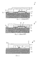
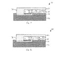
- MEMS-Schalter (30, 50, 60, 70, 80), aufweisend:ein Substrat (32);ein bewegliches Schaltelement (33, 63, 83), das mit dem Substrat (32) gekoppelt ist;einen Substratkontakt (35, 85);eine Substratelektrode (36, 56, 86); undeinen leitenden Anschlag (39, 59, 69, 79), der so aufgebaut ist, dass er eine Kontaktherstellung des beweglichen Schaltelementes (33, 63, 83) zu der Substratelektrode (36, 56, 86) verhindert, während er gleichzeitig eine Kontaktherstellung des beweglichen Schaltelementes (33, 63, 83) zu dem Substratkontakt (35, 85) zulässt; dadurch gekennzeichnet, dassder leitende Anschlag elektrisch mit dem beweglichen Schaltelement (33, 63, 83) gekoppelt ist.
- MEMS-Schalter nach Anspruch 1, wobei das bewegliche Schaltelement (33, 63, 83) und die Substratelektrode (36, 56, 86) elektrisch von dem Substrat (32) isoliert sind.
- MEMS-Schalter nach Anspruch 1 oder Anspruch 2, wobei das bewegliche Schaltelement (33, 63, 83) einen leitenden Balken aufweist.
- MEMS-Schalter nach Anspruch 3, wobei der leitende Anschlag (39, 59) einen höheren spezifischen Widerstand als der leitende Balken hat.
- MEMS-Schalter nach einem der vorstehenden Ansprüche, wobei sich der leitende Anschlag (39) auf dem Substrat (32) befindet und sich die Substratelektrode (36) zwischen dem leitenden Anschlag (39) und dem Substratkontakt (35) befindet.
- MEMS-Schalter nach Anspruch 5, wobei der leitende Anschlag (39, 59) so aufgebaut ist, sodass das bewegliche Schaltelement (33) zu dem leitenden Anschlag (39, 59) einen Kontakt herstellt, bevor es zu dem Substratkontakt (35) einen Kontakt herstellt.
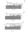
- MEMS-Schalter nach einem der vorstehenden Ansprüche, der ferner eine Leiterbahn (31, 61, 71) aufweist, die elektrisch mit dem beweglichen Schaltelement (33, 63, 83) gekoppelt ist und sich auf dem Substrat (32) wenigstens teilweise unter dem beweglichen Schaltelement (33, 63, 83) befindet.
- MEMS-Schalter nach Anspruch 7, der ferner eine Isolationsschicht (34) zwischen dem Substrat (32) und der Substratelektrode (36, 56, 86) aufweist, wobei sich die Leiterbahn (31, 61, 71) zwischen dem Substrat (32) und der Isolationsschicht (34) befindet.
- MEMS-Schalter nach Anspruch 7, wobei der leitende Anschlag (69) in das bewegliche Schaltelement (63) integriert ist, sodass, wenn das bewegliche Schaltelement (63) betätigt wird, der leitende Anschlag (69) mit der Leiterbahn (61) in Kontakt kommt.
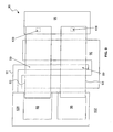
- MEMS-Schalteranordnung (90), die auf einem gemeinsamen Substrat (102) ausgebildet ist, aufweisend:ein erstes bewegliches Schaltelement (93), das mit dem Substrat (102) gekoppelt ist;ein zweites bewegliches Schaltelement (93), das mit dem Substrat (102) gekoppelt ist;eine Substratelektrode (96), die sich auf dem Substrat (102) wenigstens teilweise unter den ersten und zweiten beweglichen Schaltelementen (93) befindet;einen Substratkontakt (95), der sich auf dem Substrat (102) wenigstens teilweise unter den ersten und zweiten beweglichen Schaltelementen (93) befindet, sodass die ersten und zweiten beweglichen Schaltelemente (93) einen elektrischen Kontakt zu dem Substratkontakt (95) auf der Basis eines Zustandes der Substratelektrode (96) herstellen; undwenigstens einen leitenden Anschlag (99), der elektrisch mit den beweglichen Schaltelementen (93) gekoppelt ist und der so aufgebaut ist, dass er eine Kontaktherstellung der beweglichen Schaltelemente (93) zu der Substratelektrode (96) verhindert, während er gleichzeitig eine Kontaktherstellung der beweglichen Schaltelemente (93) zu dem Substratkontakt (95) zulässt.
Applications Claiming Priority (1)
| Application Number | Priority Date | Filing Date | Title |
|---|---|---|---|
| US11/961,767 US7609136B2 (en) | 2007-12-20 | 2007-12-20 | MEMS microswitch having a conductive mechanical stop |
Publications (2)
| Publication Number | Publication Date |
|---|---|
| EP2073236A1 EP2073236A1 (de) | 2009-06-24 |
| EP2073236B1 true EP2073236B1 (de) | 2011-03-02 |
Family
ID=40499615
Family Applications (1)
| Application Number | Title | Priority Date | Filing Date |
|---|---|---|---|
| EP08171380A Active EP2073236B1 (de) | 2007-12-20 | 2008-12-11 | MEMS-Mikroschalter mit leitfähigem Mechanikstopp |
Country Status (7)
| Country | Link |
|---|---|
| US (1) | US7609136B2 (de) |
| EP (1) | EP2073236B1 (de) |
| JP (1) | JP5449756B2 (de) |
| KR (1) | KR101538169B1 (de) |
| CN (1) | CN101533740B (de) |
| CA (1) | CA2645834A1 (de) |
| DE (1) | DE602008005244D1 (de) |
Families Citing this family (29)
| Publication number | Priority date | Publication date | Assignee | Title |
|---|---|---|---|---|
| US7754986B1 (en) * | 2007-02-27 | 2010-07-13 | National Semiconductor Corporation | Mechanical switch that reduces the effect of contact resistance |
| KR101303579B1 (ko) * | 2007-07-19 | 2013-09-09 | 삼성전자주식회사 | 전기기계적 스위치 및 그 제조방법 |
| JP4492677B2 (ja) * | 2007-11-09 | 2010-06-30 | セイコーエプソン株式会社 | アクティブマトリクス装置、電気光学表示装置、および電子機器 |
| US8779886B2 (en) * | 2009-11-30 | 2014-07-15 | General Electric Company | Switch structures |
| US8354899B2 (en) * | 2009-09-23 | 2013-01-15 | General Electric Company | Switch structure and method |
| US8576029B2 (en) | 2010-06-17 | 2013-11-05 | General Electric Company | MEMS switching array having a substrate arranged to conduct switching current |
| KR20120009574A (ko) * | 2010-07-19 | 2012-02-02 | 주식회사 코미코 | 멤스 스위치 및 이의 제조 방법 |
| FR2963784B1 (fr) * | 2010-08-11 | 2012-08-31 | Univ Limoges | Microsystemes electromecaniques a gaps d'air. |
| US8797127B2 (en) * | 2010-11-22 | 2014-08-05 | Taiwan Semiconductor Manufacturing Company, Ltd. | MEMS switch with reduced dielectric charging effect |
| JP2012196727A (ja) * | 2011-03-18 | 2012-10-18 | Fujitsu Ltd | Mems素子 |
| US9120667B2 (en) | 2011-06-20 | 2015-09-01 | International Business Machines Corporation | Micro-electro-mechanical system (MEMS) and related actuator bumps, methods of manufacture and design structures |
| WO2013011864A1 (ja) | 2011-07-15 | 2013-01-24 | 株式会社村田製作所 | 薄膜デバイスおよび薄膜デバイスの製造方法 |
| KR101273700B1 (ko) * | 2011-09-15 | 2013-06-12 | 삼성전기주식회사 | Mems 소자 |
| US9829550B2 (en) | 2012-12-27 | 2017-11-28 | General Electric Company | Multi-nuclear receiving coils for magnetic resonance imaging (MRI) |
| US20140264655A1 (en) * | 2013-03-13 | 2014-09-18 | Invensense, Inc. | Surface roughening to reduce adhesion in an integrated mems device |
| JP2016519831A (ja) * | 2013-03-14 | 2016-07-07 | インテル・コーポレーション | ナノワイヤベースのメカニカルスイッチングデバイス |
| US9136165B2 (en) * | 2013-06-04 | 2015-09-15 | Invensense, Inc. | Methods for stiction reduction in MEMS sensors |
| US9475093B2 (en) * | 2013-10-03 | 2016-10-25 | Fujifilm Dimatix, Inc. | Piezoelectric ultrasonic transducer array with switched operational modes |
| US9525119B2 (en) | 2013-12-11 | 2016-12-20 | Fujifilm Dimatix, Inc. | Flexible micromachined transducer device and method for fabricating same |
| US9748048B2 (en) * | 2014-04-25 | 2017-08-29 | Analog Devices Global | MEMS switch |
| US20160099112A1 (en) * | 2014-10-03 | 2016-04-07 | wiSpry, Inc. . | Systems, devices, and methods to reduce dielectric charging in micro-electro-mechanical systems devices |
| US9708176B2 (en) * | 2015-05-28 | 2017-07-18 | Invensense, Inc. | MEMS sensor with high voltage switch |
| JP2017073227A (ja) * | 2015-10-05 | 2017-04-13 | アルプス電気株式会社 | 磁気リードスイッチ |
| JP2017073228A (ja) * | 2015-10-05 | 2017-04-13 | アルプス電気株式会社 | 磁気リードスイッチ |
| EP3378085B1 (de) * | 2015-11-16 | 2022-11-02 | Qorvo US, Inc. | Wärmeverwaltung bei hochleistungs-rf-mems-schaltern |
| CN105702527B (zh) * | 2016-05-03 | 2018-09-21 | 北京邮电大学 | 一种微机电系统开关 |
| WO2017206149A1 (en) * | 2016-06-02 | 2017-12-07 | Goertek.Inc | Mems device and electronic apparatus |
| WO2018063814A1 (en) * | 2016-09-29 | 2018-04-05 | Cavendish Kinetics, Inc | Mems rf-switch with near-zero impact landing |
| US10416524B1 (en) * | 2017-04-25 | 2019-09-17 | University Of South Florida | Chromatic devices comprising a salt-based electrolyte |
Family Cites Families (20)
| Publication number | Priority date | Publication date | Assignee | Title |
|---|---|---|---|---|
| US6307169B1 (en) * | 2000-02-01 | 2001-10-23 | Motorola Inc. | Micro-electromechanical switch |
| US6384353B1 (en) * | 2000-02-01 | 2002-05-07 | Motorola, Inc. | Micro-electromechanical system device |
| KR100738064B1 (ko) * | 2001-02-27 | 2007-07-12 | 삼성전자주식회사 | 비선형적 복원력의 스프링을 가지는 mems 소자 |
| US6657832B2 (en) * | 2001-04-26 | 2003-12-02 | Texas Instruments Incorporated | Mechanically assisted restoring force support for micromachined membranes |
| US6646215B1 (en) * | 2001-06-29 | 2003-11-11 | Teravicin Technologies, Inc. | Device adapted to pull a cantilever away from a contact structure |
| WO2003028059A1 (en) * | 2001-09-21 | 2003-04-03 | Hrl Laboratories, Llc | Mems switches and methods of making same |
| EP1717195B1 (de) * | 2001-11-09 | 2011-09-14 | WiSpry, Inc. | MEMS-Schalter mit dreischichtigem Biegebalken und diesbezügliche Verfahren |
| US6608268B1 (en) * | 2002-02-05 | 2003-08-19 | Memtronics, A Division Of Cogent Solutions, Inc. | Proximity micro-electro-mechanical system |
| US6876282B2 (en) * | 2002-05-17 | 2005-04-05 | International Business Machines Corporation | Micro-electro-mechanical RF switch |
| US6657525B1 (en) * | 2002-05-31 | 2003-12-02 | Northrop Grumman Corporation | Microelectromechanical RF switch |
| US6686820B1 (en) * | 2002-07-11 | 2004-02-03 | Intel Corporation | Microelectromechanical (MEMS) switching apparatus |
| US6998946B2 (en) * | 2002-09-17 | 2006-02-14 | The Board Of Trustees Of The University Of Illinois | High cycle deflection beam MEMS devices |
| CN1252771C (zh) * | 2003-09-29 | 2006-04-19 | 中国科学院上海微系统与信息技术研究所 | 一种微型扭转式单刀双置射频开关结构及制作方法 |
| US7283024B2 (en) * | 2003-12-18 | 2007-10-16 | Intel Corporation | MEMS switch stopper bumps with adjustable height |
| US7352266B2 (en) * | 2004-02-20 | 2008-04-01 | Wireless Mems, Inc. | Head electrode region for a reliable metal-to-metal contact micro-relay MEMS switch |
| US20050248424A1 (en) * | 2004-05-07 | 2005-11-10 | Tsung-Kuan Chou | Composite beam microelectromechanical system switch |
| JP4504237B2 (ja) * | 2005-03-18 | 2010-07-14 | 富士通株式会社 | ウエットエッチング方法、マイクロ可動素子製造方法、およびマイクロ可動素子 |
| CN1716492A (zh) * | 2005-06-07 | 2006-01-04 | 北京邮电大学 | 集成方式的rf mems开关 |
| US7385744B2 (en) * | 2006-06-28 | 2008-06-10 | Qualcomm Mems Technologies, Inc. | Support structure for free-standing MEMS device and methods for forming the same |
| JP2008238330A (ja) * | 2007-03-27 | 2008-10-09 | Toshiba Corp | Mems装置およびこのmems装置を有する携帯通信端末 |
-
2007
- 2007-12-20 US US11/961,767 patent/US7609136B2/en active Active
-
2008
- 2008-12-04 CA CA002645834A patent/CA2645834A1/en not_active Abandoned
- 2008-12-11 DE DE602008005244T patent/DE602008005244D1/de active Active
- 2008-12-11 EP EP08171380A patent/EP2073236B1/de active Active
- 2008-12-12 JP JP2008316853A patent/JP5449756B2/ja active Active
- 2008-12-18 KR KR1020080129356A patent/KR101538169B1/ko active IP Right Grant
- 2008-12-22 CN CN200810188424XA patent/CN101533740B/zh active Active
Also Published As
| Publication number | Publication date |
|---|---|
| JP2009152194A (ja) | 2009-07-09 |
| CA2645834A1 (en) | 2009-06-20 |
| EP2073236A1 (de) | 2009-06-24 |
| DE602008005244D1 (de) | 2011-04-14 |
| KR101538169B1 (ko) | 2015-07-20 |
| US7609136B2 (en) | 2009-10-27 |
| CN101533740B (zh) | 2013-11-13 |
| CN101533740A (zh) | 2009-09-16 |
| JP5449756B2 (ja) | 2014-03-19 |
| KR20090067080A (ko) | 2009-06-24 |
| US20090159410A1 (en) | 2009-06-25 |
Similar Documents
| Publication | Publication Date | Title |
|---|---|---|
| EP2073236B1 (de) | MEMS-Mikroschalter mit leitfähigem Mechanikstopp | |
| US7692519B2 (en) | MEMS switch with improved standoff voltage control | |
| US8093971B2 (en) | Micro-electromechanical system switch | |
| EP2073237B1 (de) | MEMS-Mikroschalter mit Doppelbetätigung und gemeinsamen Zugang | |
| US8570705B2 (en) | MEMS sprung cantilever tunable capacitors and methods | |
| KR20010030305A (ko) | 접이식 스프링을 구비한 초소형 전기 기계 고주파 스위치및 그 제조 방법 | |
| US7928333B2 (en) | Switch structures | |
| US20030082917A1 (en) | Method of fabricating vertical actuation comb drives | |
| KR20040053127A (ko) | 미소기계 스위치 및 그 제조 방법 | |
| KR100977917B1 (ko) | 마이크로-전자기계 시스템을 갖춘 마이크로스위치 | |
| JP2003323840A (ja) | リレー |
Legal Events
| Date | Code | Title | Description |
|---|---|---|---|
| PUAI | Public reference made under article 153(3) epc to a published international application that has entered the european phase |
Free format text: ORIGINAL CODE: 0009012 |
|
| AK | Designated contracting states |
Kind code of ref document: A1 Designated state(s): AT BE BG CH CY CZ DE DK EE ES FI FR GB GR HR HU IE IS IT LI LT LU LV MC MT NL NO PL PT RO SE SI SK TR |
|
| AX | Request for extension of the european patent |
Extension state: AL BA MK RS |
|
| RIN1 | Information on inventor provided before grant (corrected) |
Inventor name: BOOMHOWER, OLIVER CHARLES Inventor name: CLAYDON, GLENN SCOTT Inventor name: SUBRAMANIAN, KANAKASABAPATHI Inventor name: THAKRE, PARAG Inventor name: WANG, XUEFENG Inventor name: KEIMEL, CHRISTOPHER FRED Inventor name: KISHORE, KUNA VENKAT SATYA RAMA Inventor name: AIMI, MARCO FRANCESCO |
|
| 17P | Request for examination filed |
Effective date: 20091228 |
|
| AKX | Designation fees paid |
Designated state(s): DE FR GB IT |
|
| GRAP | Despatch of communication of intention to grant a patent |
Free format text: ORIGINAL CODE: EPIDOSNIGR1 |
|
| GRAS | Grant fee paid |
Free format text: ORIGINAL CODE: EPIDOSNIGR3 |
|
| GRAA | (expected) grant |
Free format text: ORIGINAL CODE: 0009210 |
|
| AK | Designated contracting states |
Kind code of ref document: B1 Designated state(s): DE FR GB IT |
|
| REG | Reference to a national code |
Ref country code: GB Ref legal event code: FG4D |
|
| REF | Corresponds to: |
Ref document number: 602008005244 Country of ref document: DE Date of ref document: 20110414 Kind code of ref document: P |
|
| REG | Reference to a national code |
Ref country code: DE Ref legal event code: R096 Ref document number: 602008005244 Country of ref document: DE Effective date: 20110414 |
|
| PLBE | No opposition filed within time limit |
Free format text: ORIGINAL CODE: 0009261 |
|
| STAA | Information on the status of an ep patent application or granted ep patent |
Free format text: STATUS: NO OPPOSITION FILED WITHIN TIME LIMIT |
|
| 26N | No opposition filed |
Effective date: 20111205 |
|
| REG | Reference to a national code |
Ref country code: DE Ref legal event code: R097 Ref document number: 602008005244 Country of ref document: DE Effective date: 20111205 |
|
| PGFP | Annual fee paid to national office [announced via postgrant information from national office to epo] |
Ref country code: DE Payment date: 20131230 Year of fee payment: 6 Ref country code: GB Payment date: 20131227 Year of fee payment: 6 |
|
| REG | Reference to a national code |
Ref country code: DE Ref legal event code: R119 Ref document number: 602008005244 Country of ref document: DE |
|
| GBPC | Gb: european patent ceased through non-payment of renewal fee |
Effective date: 20141211 |
|
| PG25 | Lapsed in a contracting state [announced via postgrant information from national office to epo] |
Ref country code: GB Free format text: LAPSE BECAUSE OF NON-PAYMENT OF DUE FEES Effective date: 20141211 Ref country code: DE Free format text: LAPSE BECAUSE OF NON-PAYMENT OF DUE FEES Effective date: 20150701 |
|
| REG | Reference to a national code |
Ref country code: FR Ref legal event code: PLFP Year of fee payment: 8 |
|
| REG | Reference to a national code |
Ref country code: FR Ref legal event code: PLFP Year of fee payment: 9 |
|
| PG25 | Lapsed in a contracting state [announced via postgrant information from national office to epo] |
Ref country code: IT Free format text: LAPSE BECAUSE OF NON-PAYMENT OF DUE FEES Effective date: 20151211 |
|
| PG25 | Lapsed in a contracting state [announced via postgrant information from national office to epo] |
Ref country code: IT Free format text: LAPSE BECAUSE OF NON-PAYMENT OF DUE FEES Effective date: 20151211 |
|
| PGRI | Patent reinstated in contracting state [announced from national office to epo] |
Ref country code: IT Effective date: 20170710 |
|
| REG | Reference to a national code |
Ref country code: FR Ref legal event code: PLFP Year of fee payment: 10 |
|
| PGFP | Annual fee paid to national office [announced via postgrant information from national office to epo] |
Ref country code: IT Payment date: 20221122 Year of fee payment: 15 |
|
| PGFP | Annual fee paid to national office [announced via postgrant information from national office to epo] |
Ref country code: FR Payment date: 20231122 Year of fee payment: 16 |