EP2073236B1 - MEMS Microswitch having a conductive mechanical stop - Google Patents
MEMS Microswitch having a conductive mechanical stop Download PDFInfo
- Publication number
- EP2073236B1 EP2073236B1 EP08171380A EP08171380A EP2073236B1 EP 2073236 B1 EP2073236 B1 EP 2073236B1 EP 08171380 A EP08171380 A EP 08171380A EP 08171380 A EP08171380 A EP 08171380A EP 2073236 B1 EP2073236 B1 EP 2073236B1
- Authority
- EP
- European Patent Office
- Prior art keywords
- substrate
- conductive
- movable actuator
- contact
- movable
- Prior art date
- Legal status (The legal status is an assumption and is not a legal conclusion. Google has not performed a legal analysis and makes no representation as to the accuracy of the status listed.)
- Active
Links
- 239000000758 substrate Substances 0.000 claims description 151
- 238000002955 isolation Methods 0.000 claims description 9
- 239000004020 conductor Substances 0.000 description 6
- 238000000034 method Methods 0.000 description 5
- 239000000463 material Substances 0.000 description 4
- 229910001020 Au alloy Inorganic materials 0.000 description 3
- 229910045601 alloy Inorganic materials 0.000 description 3
- 239000000956 alloy Substances 0.000 description 3
- PCHJSUWPFVWCPO-UHFFFAOYSA-N gold Chemical compound [Au] PCHJSUWPFVWCPO-UHFFFAOYSA-N 0.000 description 3
- 239000010931 gold Substances 0.000 description 3
- 229910052737 gold Inorganic materials 0.000 description 3
- 239000003353 gold alloy Substances 0.000 description 3
- 239000000203 mixture Substances 0.000 description 3
- 230000008859 change Effects 0.000 description 2
- 239000012212 insulator Substances 0.000 description 2
- BASFCYQUMIYNBI-UHFFFAOYSA-N platinum Chemical compound [Pt] BASFCYQUMIYNBI-UHFFFAOYSA-N 0.000 description 2
- 230000008569 process Effects 0.000 description 2
- 229910000838 Al alloy Inorganic materials 0.000 description 1
- 229910001260 Pt alloy Inorganic materials 0.000 description 1
- 229910052581 Si3N4 Inorganic materials 0.000 description 1
- VYPSYNLAJGMNEJ-UHFFFAOYSA-N Silicium dioxide Chemical compound O=[Si]=O VYPSYNLAJGMNEJ-UHFFFAOYSA-N 0.000 description 1
- 238000009825 accumulation Methods 0.000 description 1
- XAGFODPZIPBFFR-UHFFFAOYSA-N aluminium Chemical compound [Al] XAGFODPZIPBFFR-UHFFFAOYSA-N 0.000 description 1
- QRJOYPHTNNOAOJ-UHFFFAOYSA-N copper gold Chemical compound [Cu].[Au] QRJOYPHTNNOAOJ-UHFFFAOYSA-N 0.000 description 1
- 230000008878 coupling Effects 0.000 description 1
- 238000010168 coupling process Methods 0.000 description 1
- 238000005859 coupling reaction Methods 0.000 description 1
- 230000001419 dependent effect Effects 0.000 description 1
- 238000005516 engineering process Methods 0.000 description 1
- 229910052732 germanium Inorganic materials 0.000 description 1
- GNPVGFCGXDBREM-UHFFFAOYSA-N germanium atom Chemical compound [Ge] GNPVGFCGXDBREM-UHFFFAOYSA-N 0.000 description 1
- 238000009413 insulation Methods 0.000 description 1
- 230000007257 malfunction Effects 0.000 description 1
- 229910001092 metal group alloy Inorganic materials 0.000 description 1
- TWNQGVIAIRXVLR-UHFFFAOYSA-N oxo(oxoalumanyloxy)alumane Chemical compound O=[Al]O[Al]=O TWNQGVIAIRXVLR-UHFFFAOYSA-N 0.000 description 1
- 230000004044 response Effects 0.000 description 1
- 229910052710 silicon Inorganic materials 0.000 description 1
- 239000010703 silicon Substances 0.000 description 1
- HQVNEWCFYHHQES-UHFFFAOYSA-N silicon nitride Chemical compound N12[Si]34N5[Si]62N3[Si]51N64 HQVNEWCFYHHQES-UHFFFAOYSA-N 0.000 description 1
- 229910052814 silicon oxide Inorganic materials 0.000 description 1
Images
Classifications
-
- H—ELECTRICITY
- H01—ELECTRIC ELEMENTS
- H01H—ELECTRIC SWITCHES; RELAYS; SELECTORS; EMERGENCY PROTECTIVE DEVICES
- H01H59/00—Electrostatic relays; Electro-adhesion relays
- H01H59/0009—Electrostatic relays; Electro-adhesion relays making use of micromechanics
-
- B—PERFORMING OPERATIONS; TRANSPORTING
- B81—MICROSTRUCTURAL TECHNOLOGY
- B81B—MICROSTRUCTURAL DEVICES OR SYSTEMS, e.g. MICROMECHANICAL DEVICES
- B81B7/00—Microstructural systems; Auxiliary parts of microstructural devices or systems
- B81B7/02—Microstructural systems; Auxiliary parts of microstructural devices or systems containing distinct electrical or optical devices of particular relevance for their function, e.g. microelectro-mechanical systems [MEMS]
-
- B—PERFORMING OPERATIONS; TRANSPORTING
- B81—MICROSTRUCTURAL TECHNOLOGY
- B81B—MICROSTRUCTURAL DEVICES OR SYSTEMS, e.g. MICROMECHANICAL DEVICES
- B81B7/00—Microstructural systems; Auxiliary parts of microstructural devices or systems
-
- H—ELECTRICITY
- H01—ELECTRIC ELEMENTS
- H01H—ELECTRIC SWITCHES; RELAYS; SELECTORS; EMERGENCY PROTECTIVE DEVICES
- H01H59/00—Electrostatic relays; Electro-adhesion relays
-
- H—ELECTRICITY
- H01—ELECTRIC ELEMENTS
- H01H—ELECTRIC SWITCHES; RELAYS; SELECTORS; EMERGENCY PROTECTIVE DEVICES
- H01H59/00—Electrostatic relays; Electro-adhesion relays
- H01H59/0009—Electrostatic relays; Electro-adhesion relays making use of micromechanics
- H01H2059/0072—Electrostatic relays; Electro-adhesion relays making use of micromechanics with stoppers or protrusions for maintaining a gap, reducing the contact area or for preventing stiction between the movable and the fixed electrode in the attracted position
Description
- Embodiments of the invention relate generally to a micro-electromechanical system (MEMS) switch having a conductive mechanical stop.
- Microelectromechanical systems (MEMS) are electromechanical devices that generally range in size from a micrometer to a millimeter in a miniature sealed package. A MEMS device in the form of a microswitch has a movable actuator, also referred to as a beam, that is moved toward a stationary electrical contact by the influence of a gate or substrate electrode positioned on a substrate below or otherwise near the movable actuator. The movable actuator may be a flexible beam that bends under applied forces such as electrostatic attraction, magnetic attraction and repulsion, or thermally induced differential expansion, that closes a gap between a free end of the beam and the stationary contact.
-
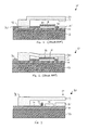
FIG. 1 illustrates a cross-sectional representation of a MEMS switch in an open or non-conducting state according to the prior art. TheMEMS switch 10 includes asubstrate 12, aninsulating layer 14 disposed over thesubstrate 12 and amovable actuator 23 mechanically coupled or anchored to asource electrode 18 as shown. Themovable actuator 23 includes a movable contact 17, which upon deflection of themovable actuator 23 makes contact with asubstrate contact 15 disposed on but electrically isolated from thesubstrate 12. Thesubstrate electrode 16 is positioned below themovable actuator 23 such that when an actuation voltage is applied to thesubstrate electrode 16, themovable actuator 23 deflects such that contact is made between the movable and stationary (e.g., substrate) contacts to allow current to flow. In order to keep the conductivemovable actuator 23 from contacting thesubstrate electrode 16 and electrically shorting the switch when in such a conducting state, adielectric layer 20 is typically coated over thesubstrate electrode 16 as illustrated inFIG. 2 . This dielectric layer is often disposed over thesubstrate electrode 16 but it may instead be coated on the underside of themovable actuator 23. - However, such a dielectric insulation layer can trap charge over time and negatively affect the operation of the actuator such as causing it to malfunction (e.g., cause stiction of the electrode), change the actuation and stand-off voltages, change the response time of the switch, shorten its operating lifetime, and so forth. This can be especially problematic in power conduction applications where inadvertent actuation can cause undesirable conduction modes and/or switch damage.
- Document
US6307169 discloses a device according to the preamble ofclaim 1. - In one embodiment, a MEMS switch includes a substrate, a movable actuator coupled to the substrate, a substrate contact, a substrate electrode; and a conductive stopper electrically coupled to the movable actuator and structured to prevent the movable actuator from contacting the substrate electrode while allowing the movable actuator to make contact with the substrate contact.
- In another embodiment, a MEMS switch includes a substrate, a movable actuator coupled to the substrate, a substrate contact, a substrate electrode, and a conductive stopper located on the substrate and electrically coupled to the movable actuator such that the conductive stopper and the movable actuator maintain the same electrical potential.
- In a further embodiment, a MEMS switch includes a substrate, a movable actuator coupled to the substrate and comprising a conductive stopper, a substrate contact, a substrate electrode, and a conductive trace electrically coupled to the movable actuator and located on the substrate at least partially below the movable actuator such that the conductive stopper makes electrical contact with the conductive trace and the movable actuator makes electrical contact with the substrate contact when the switch is actuated.
- In yet a further embodiment, a MEMS switch array formed on a shared substrate is provided. The switch array includes a first movable actuator coupled to the substrate, a second movable actuator coupled to the substrate, a substrate electrode located on the substrate at least partially below the first and second movable actuators, and a substrate contact located on the substrate at least partially below the first and second movable actuators such that the first and second movable actuators make electrical contact with the substrate contact based upon a state of the substrate electrode. The switch array further includes at least one conductive stopper electrically coupled to the movable actuators and structured to prevent the movable actuators from contacting the substrate electrode while allowing the movable actuators to make contact with the substrate contact.
- These and other features, aspects, and advantages of the present invention will become better understood when the following detailed description is read with reference to the accompanying drawings in which like characters represent like parts throughout the drawings, wherein:
-
FIG. 1 illustrates a cross-sectional representation of a MEMS switch in an open or non-conducting state according to the prior art; -
FIG. 2 illustrates a cross-sectional representation of aMEMS switch 10 in an actuated state according to the prior art; -
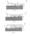
FIG. 3 illustrates a cross-sectional representation of aMEMS switch 30 including a conductive mechanical stop in an open state, in accordance with one embodiment of the invention; -
FIG. 4 illustrates a cross-sectional representation of theMEMS switch 30 including a conductive mechanical stop in an actuated state, in accordance with one embodiment of the invention; -
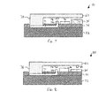
FIG. 5 illustrates a cross-sectional representation of a MEMS switch including more than one conductive mechanical stop, in accordance with one embodiment of the invention; -
FIG. 6 illustrates a cross-sectional representation of a MEMS switch including a movable actuator having a conductive stopper, in accordance with one embodiment of the invention; -
FIG. 7 illustrates a cross-sectional representation of a MEMS switch having a split conductive stopper, in accordance with one embodiment of the invention; -
FIG. 8 illustrates a cross-sectional representation of a MEMS switch having a split conductive stopper and a conductive contact bump, in accordance with one embodiment of the invention; and -
FIG. 9 illustrates one embodiment of a MEMS switch array including at least two MEMS switches with at least one conductive stopper. - In accordance with embodiments of the invention, a MEMS switch and switch array are described wherein the conventional dielectric insulator that traditionally separates the substrate electrode from the movable actuator is removed. In accordance with various embodiments of the invention, a conductive stopper is provided that is electrically coupled to the movable actuator and structured to prevent the movable actuator from contacting the substrate electrode while allowing the movable actuator to make contact with the substrate contact. Since the conductive stopper prevents the movable actuator from making contact with the substrate electrode, the dielectric insulator used in conventional MEMS switches can be removed thereby eliminating a source of undesirable charge accumulation and increasing the standoff voltage of the MEMS switch described herein. Furthermore, by electrically coupling the movable actuator and the conductive stopper, they can be maintained at the same electrical potential thereby minimizing chances of arcing between the movable actuator and the conductive stopper to which convention MEMS switches are susceptible.
- In the following detailed description, numerous specific details are set forth in order to provide a thorough understanding of various embodiments of the present invention. However, those skilled in the art will understand that embodiments of the present invention may be practiced without these specific details, that the present invention is not limited to the depicted embodiments, and that the present invention may be practiced in a variety of alternative embodiments. In other instances, well known methods, procedures, and components have not been described in detail.
- Furthermore, various operations may be described as multiple discrete steps performed in a manner that is helpful for understanding embodiments of the present invention. However, the order of description should not be construed as to imply that these operations need be performed in the order they are presented, nor that they are even order dependent. Moreover, repeated usage of the phrase "in one embodiment" does not necessarily refer to the same embodiment, although it may. Lastly, the terms "comprising", "including", "having", and the like, as well as their inflected forms as used in the present application, are intended to be synonymous unless otherwise indicated.
- MEMS generally refer to micron-scale structures that can integrate a multiplicity of functionally distinct elements such as mechanical elements, electromechanical elements, sensors, actuators, and electronics, on a common substrate through microfabrication technology. It is contemplated, however, that many techniques and structures presently available in MEMS devices will in just a few years be available via nanotechnology-based devices, for example, structures that may be smaller than 100 nanometers in size. Accordingly, even though example embodiments described throughout this document may refer to MEMS-based switching devices, it is submitted that the embodiments should be broadly construed and should not be limited to only micron-sized devices unless otherwise limited to such.
-
FIG. 3 illustrates a cross-sectional representation of aMEMS switch 30 including a conductive mechanical stop in accordance with one embodiment of the invention. In the illustrated embodiment,MEMS switch 30 includes asubstrate 32 which may be conductive, semi-conductive or insulating. In an embodiment where thesubstrate 32 is conductive, the substrate may be coated with an insulating orelectrical isolation layer 34 to prevent undesirable shorting between and amongst substrate electrodes and substrate contacts (to be described further below). Non-limiting examples of conducting substrates include those formed from silicon and germanium, whereas non-limiting examples of an electrical isolation layer include silicon nitride, silicon oxide, and aluminum oxide. - The
MEMS switch 30 further includes a movable actuator 33 (often referred to as a beam) that is mechanically coupled or anchored to thesubstrate 32 by ananchor 38. In one embodiment, themovable actuator 33 is conductive such that current can flow from a "source" contact (not illustrated) at the base of theanchor 38, through themovable actuator 33, and through to a substrate contact 35 (sometimes referred to as a drain contact). In one embodiment, themovable actuator 33 is formed from gold or a gold alloy, however, themovable actuator 33 may further include resistive or non-conducting materials and one or more stress compensation layers depending upon the design of the MEMS switch. Similarly, thesubstrate contact 35 may be formed from a variety of conductive materials or compositions or alloys thereof. In one embodiment, thesubstrate contact 35 may be made from gold or a gold alloy for example. Thesubstrate 32 may be biased at any desired electrical potential. In one embodiment, to reduce any attraction force (e.g., such as but not limited to electrostatic and magnetic attraction forces) between the substrate and themovable actuator 33, the substrate may be biased at the same electrical potential as themovable actuator 33. This can be achieved through a substrate contact electrode or by electrically connecting theanchor 38 to thesubstrate 32. - In the illustrated embodiment, the
MEMS switch 30 further includes asubstrate electrode 36. Thesubstrate electrode 36 may also comprise one or more conductive materials, compositions or alloys thereof. As with thesubstrate contact 35, thesubstrate electrode 36 may similarly be made from gold or a gold alloy. Moreover, thesubstrate electrode 36 and thesubstrate contact 35 may be formed from the same photolithographic process mask. In one embodiment, the conductive material of thesubstrate electrode 36 is left exposed without the addition of a dielectric layer traditionally used to prevent direct contact between movable actuators and substrate electrodes. Moreover, in accordance with one embodiment, the bottom surface of themovable actuator 33 may further include an exposed conductive surface opposite the exposed conductive surface of thesubstrate electrode 36. - In the illustrated embodiment,
movable actuator 33 represents a cantilever beam having a stationary end (e.g., anchor 38) and amovable end 37, which deflects towardsubstrate 32 upon application of a voltage differential between thesubstrate electrode 36 and themovable actuator 33. However, the teachings herein may similarly apply to other forms of MEMS switches beyond those depicted in the Figures. For example, themovable actuator 33 could be anchored at two or more ends or sides resembling a bridge or diaphragm type switch. Similarly, the actuation of themovable actuator 33 may be substantially out of plane (e.g., perpendicular to the substrate) as shown in the Figures, or substantially in-plane (e.g., parallel to the substrate). - In accordance with one embodiment of the invention, one or more conductive stoppers are provided to prevent the movable actuator from contacting one or more substrate electrodes while allowing the movable actuator to make contact with the substrate contact upon actuation. As illustrated in
FIG. 3 andFIG. 4 , aconductive stopper 39 may be provided on thesubstrate 32 so as to prevent themovable actuator 33 from contacting thesubstrate electrode 36 while allowing themovable actuator 33 to deflect at themovable end 37 to make contact with thesubstrate contact 35 upon actuation of the switch. Theconductive stopper 39 may include one or more conductive materials or compositions or alloys thereof. Further, theconductive stopper 39 may be formed from the same material as themovable actuator 33 or from a different material. In an embodiment where theconductive stopper 39 and themovable actuator 33 are fabricated from different materials, theconductive stopper 39 may he designed to have a higher resistivity than themovable actuator 33 so as to decrease the chance of arcing between theconductive stopper 39 and themovable actuator 33. - Each
conductive stopper 39 can be fabricated on the substrate (e.g., as shown inFIGS. 3 .4 and 5 ), or as part of the movable actuator (e.g., as shown inFIG. 6 ), or may be divided into two parts (e.g., as shown inFIG. 7 and 8 ) with a first portion formed on the substrate and at least one other portion formed as part of themovable actuator 33. In an embodiment where theconductive stopper 39 is formed on the substrate, the conductive stopper can be formed using the same photolithographic process mask as may be used for forming thesubstrate contact 35 or thesubstrate electrode 36. - In one embodiment, the
conductive stop 39 may be positioned such that thesubstrate electrode 36 is located between thesubstrate contact 35 and theconductive stopper 39. The closer the substrate electrode is to the substrate contact the more force that is available to pull the movable actuator towards the substrate contact. By positioning theconductive stop 39 such that one ormore substrate electrodes 36 are located between thesubstrate contact 35 and theconductive stop 39, it is possible to increase the actuation force at themovable end 37 to provide better contact between themovable actuator 33 and thesubstrate contact 35. Optionally, in any of the embodiments described herein, an additional conductive contact may be provided on themovable end 37 of themovable actuator 33. - In accordance with one embodiment, the form factor of the
conductive stopper 39 may be varied depending upon a variety of factors. For example, a conductive stopper for a single MEMS switch may resemble a pillar or post, whereas a conductive stopper for a switch array may resemble a beam. In one embodiment, the conductive stopper may have a height (e.g., the dimension extending toward the movable actuator 33) that is greater than its length or width. In one embodiment, theconductive stopper 39 may be structured such that themoveable electrode 33 contacts thesubstrate contact 35 before it contacts the conductive stopper. In an alternative embodiment, theconductive stopper 39 may be structured such that themoveable electrode 33 contacts thesubstrate contact 35 at substantially the same time as it contacts the conductive stopper. In yet another alternative embodiment, theconductive stopper 39 may be structured such that themoveable electrode 33 first contacts theconductive stopper 39 before contacting thesubstrate contact 35. In such an embodiment, theconductive stopper 39 may have a height that is greater than that of thesubstrate contact 35. By fabricating theconductive stopper 39 to be taller (e.g., closer to the movable actuator) than thesubstrate contact 35, it is possible to increase the effective resonant frequency of themovable contact 33 resulting in faster parting between thesubstrate contact 35 and themovable actuator 33. Furthermore, by making theconductive stopper 39 taller than thesubstrate contact 35, themovable actuator 33 will contact theconductive stopper 39 first requiring an increased pull-in voltage to actuate the beam. - In one embodiment, the
conductive stopper 39 is electrically coupled to themovable actuator 33 to maintain the same electrical potential between theconductive stopper 39 and themovable actuator 33. In power conduction applications for example, this can be a desirable feature as themovable actuator 33 and themechanical stop 39 can otherwise be at different electrical potentials. The resulting potential difference could in turn generate an attraction force between themechanical stop 39 and themovable actuator 33. This may cause themovable actuator 33 to actuate or deflect at undesirable times, in turn reducing the standoff voltage of the switch. In one embodiment, one or more mechanical stops, such asmechanical stop 39, may be electrically coupled to themovable contact 33 byconductive trace 31. In one embodiment, theconductive trace 31 may be routed on the surface of or otherwise above theelectrical isolation layer 34 at least partially below themovable actuator 33. In another embodiment, theconductive trace 31 may be routed between theelectrical isolation layer 34 and thesubstrate 32. Theconductive trace 34 may be formed from one or more conductive material such as copper gold, aluminum, platinum, or metal alloys. -
FIG. 5 illustrates a cross-sectional representation of a MEMS switch including more than one conductive mechanical stop, in accordance with one embodiment of the invention. As illustrated. MEMS switch 50 includes at least one additional conductive stopper 59. Conductive stopper 59 may be substantially similar in materials and design asconductive stopper 39. Alternatively, the conductive stopper 59 and theconductive stopper 39 may have different form factors (including heights) depending upon the desired application. In one embodiment, the conductive stopper 59 and theconductive stopper 39 may be electrically coupled to themovable actuator 33 by aconductive trace 51 which may be substantially similar in design to the previously describedconductive trace 31. Additionally, MEMS switch 50 may further include one or more additional substrate electrodes such as the substrate electrode 56 depicted inFIG. 5 . Each such additional substrate electrode may be substantially similar in form and function as the previously describedsubstrate electrode 36. -
FIG. 6 illustrates a cross-sectional representation of a MEMS switch including a movable actuator having a conductive stopper, in accordance with one embodiment of the invention. As with the previously described MEMS switch embodiments,MEMS switch 60 includes asubstrate 32, anelectrical isolation layer 34, asubstrate contact 35 and asubstrate electrode 36. However, rather than including a conductive stopper that is formed as part of the substrate portion,MEMS switch 60 includes a movableconductive stopper 69 that is coupled to or otherwise integrated with themovable actuator 63. Additionally, aconductive trace 61 is provided that is routed from a location approximately below theconductive stopper 69 to the movable actuator 63 (e.g., by way of anchor 38) such that theconductive stopper 69 contacts theconductive trace 61 upon actuation of the switch. In one embodiment, the distance separating theconductive stopper 69 from theconductive trace 61 is the same as the distance separating themovable actuator 63 from thesubstrate contact 35. -
FIG. 7 illustrates a cross-sectional representation of a MEMS switch having a split conductive stopper, in accordance with one embodiment of the invention. In the illustrated embodiment, aMEMS switch 70 is shown having a split or divided conductive stopper including a firstmovable portion 79a coupled to or integrated with themovable contact 63, and a stationarysecond portion 79b coupled to the substrate and positioned to make contact with the firstmovable portion 79a upon actuation of theswitch 70. In one embodiment, the stationarysecond portion 79b may further be electrically coupled to the movable actuator by aconductive trace 71. As with the previously described conductive traces (31, 51, 61),conductive trace 71 may be routed on top of or belowelectrical isolation layer 34. -
Fig. 8 illustrates a cross-sectional representation of a MEMS switch having a split conductive stopper and a conductive contact bump, in accordance with one embodiment of the invention. As with theMEMS switch 70, theMEMS switch 80 may further include a split conductive stopper having a firstmovable portion 79a on the movable actuator 83 and a secondstationary portion 79b positioned below the movable portion. In addition, theMEMS switch 80 may further include a protrusion such as a conductive contact bump 89 on the movable actuator 83, which upon actuation of the movable actuator 83 makes contact with thesubstrate contact 85. With the addition of conductive contact bump 89, it is possible to have a substrate electrode (such as substrate electrode 86) with a height that is greater than the height of the substrate contact as illustrated. -
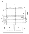
FIG. 9 illustrates one embodiment of aMEMS switch array 90 including two MEMS switches 98 each having with at least oneconductive stopper 99. For the purposes of explanation, only two MEMS switches are illustrated in theMEMS switch array 90. However, although not illustrated,MEMS switch array 90 may include a large number of MEMS switches coupled in series, parallel, or series-parallel arrangements. Each MEMS switch inMEMS switch array 90 includes twomovable actuators 93 anchored to a "source"contact 100 disposed on asubstrate 102. Themovable actuators 93 extend or are cantilevered oversubstrate electrode 96 and substrate contact 95 also located on thesubstrate 102. As previously described, thesubstrate 102 may further include an electrical isolation layer (not shown) disposed between thesubstrate 102 and one or more of thesubstrate electrode 96, the substrate contact 95 and thesource electrode 100 oranchor 98. - In accordance with one embodiment, each MEMS switch further includes a
conductive stopper 99. As previously described, theconductive stoppers 99 may be fabricated on thesubstrate 102, on themovable actuator 93 or partly on thesubstrate 102 and partly on themovable actuator 93. In an embodiment where theconductive stopper 99 is fabricated at least partly on thesubstrate 102, theconductive stopper 99 may be electrically coupled to themovable actuator 93 by way of theconductive trace 91 and thesource contact 100 and/or theanchor 98. In an embodiment where theconductive stopper 99 is fabricated at least partly on the movable actuator, theconductive stopper 99 may be electrically conducted to theconductive trace 91 only upon actuation of the switch. Additionally, each MEMS switch may further include one or more conductive contact bumps 109 included on the underside ofmovable actuator 93.
Claims (10)
- A MEMS switch (30,50,60,70,80) comprising:a substrate (32);a movable actuator (33,63,83) coupled to the substrate (32);a substrate contact (35,85);a substrate electrode (36,56,86); anda conductive stopper (39,59,69,79) structured to prevent the movable actuator (33,63,83) from contacting the substrate electrode (36,56,86) while allowing the movable actuator (33, 63,83) to make contact with the substrate contact (35,85), characterised in that the conductive stopper is electrically coupled to the movable actuator (33,63,83).
- The MEMS switch of claim 1, wherein the movable actuator (33,63,83) and the substrate electrode (36,56,86) are electrically isolated from the substrate (32).
- The MEMS switch of claim 1 or claim 2, wherein the movable actuator (33, 63,83) comprises a conductive beam.
- The MEMS switch of claim 3, wherein the conductive stopper (39,59) has a higher resistivity than the conductive beam.
- The MEMS switch of any one of the preceding claims, wherein the conductive stopper (39) is located on the substrate (32) and the substrate electrode (36) is located between the conductive stopper (39) and the substrate contact (35).
- The MEMS switch of claim 5, wherein conductive stopper (39,59) is structured such that the movable actuator (33) makes contact with the conductive stopper (39,59) before it makes contact with the substrate contact (35).
- The MEMS switch of any of the preceding claims, further comprising a conductive trace (31,61,71) electrically coupled to the movable actuator (33,63,83) and located on the substrate (32) at least partially under the movable actuator (33,63, 83).
- The MEMS switch of claim 7, further comprising an isolation layer (34) between the substrate (32) and the substrate electrode (36,56,86) wherein the conductive trace (31,61,71) is located between the substrate (32) and the isolation layer (34).
- The MEMS switch of claim 7, wherein the conductive stopper (69) is integrated with the movable actuator (63) such that when the movable actuator (63) is actuated, the conductive stopper (69) contacts the conductive trace (61).
- A MEMS switch array (90) formed on a shared substrate (102) comprising:a first movable actuator (93) coupled to the substrate (102);a second movable actuator (93) coupled to the substrate (102);a substrate electrode (96) located on the substrate (102) at least partially below the first and second movable actuators (93);a substrate contact (95) located on the substrate (102) at least partially below the first and second movable actuators (93) such that the first and second movable actuators (93) make electrical contact with the substrate contact (95) based upon a state of the substrate electrode (96); andat least one conductive stopper (99) electrically coupled to the movable actuators (93) and structured to prevent the movable actuators (93) from contacting the substrate electrode (96) while allowing the movable actuators (93) to make contact with the substrate contact (95).
Applications Claiming Priority (1)
| Application Number | Priority Date | Filing Date | Title |
|---|---|---|---|
| US11/961,767 US7609136B2 (en) | 2007-12-20 | 2007-12-20 | MEMS microswitch having a conductive mechanical stop |
Publications (2)
| Publication Number | Publication Date |
|---|---|
| EP2073236A1 EP2073236A1 (en) | 2009-06-24 |
| EP2073236B1 true EP2073236B1 (en) | 2011-03-02 |
Family
ID=40499615
Family Applications (1)
| Application Number | Title | Priority Date | Filing Date |
|---|---|---|---|
| EP08171380A Active EP2073236B1 (en) | 2007-12-20 | 2008-12-11 | MEMS Microswitch having a conductive mechanical stop |
Country Status (7)
| Country | Link |
|---|---|
| US (1) | US7609136B2 (en) |
| EP (1) | EP2073236B1 (en) |
| JP (1) | JP5449756B2 (en) |
| KR (1) | KR101538169B1 (en) |
| CN (1) | CN101533740B (en) |
| CA (1) | CA2645834A1 (en) |
| DE (1) | DE602008005244D1 (en) |
Families Citing this family (29)
| Publication number | Priority date | Publication date | Assignee | Title |
|---|---|---|---|---|
| US7754986B1 (en) * | 2007-02-27 | 2010-07-13 | National Semiconductor Corporation | Mechanical switch that reduces the effect of contact resistance |
| KR101303579B1 (en) * | 2007-07-19 | 2013-09-09 | 삼성전자주식회사 | Electromechanical switch and method of manufacturing the same |
| JP4492677B2 (en) * | 2007-11-09 | 2010-06-30 | セイコーエプソン株式会社 | Active matrix device, electro-optical display device, and electronic apparatus |
| US8354899B2 (en) * | 2009-09-23 | 2013-01-15 | General Electric Company | Switch structure and method |
| US8779886B2 (en) * | 2009-11-30 | 2014-07-15 | General Electric Company | Switch structures |
| US8576029B2 (en) * | 2010-06-17 | 2013-11-05 | General Electric Company | MEMS switching array having a substrate arranged to conduct switching current |
| KR20120009574A (en) * | 2010-07-19 | 2012-02-02 | 주식회사 코미코 | MEMS switch and manufacturing method of the same |
| FR2963784B1 (en) * | 2010-08-11 | 2012-08-31 | Univ Limoges | ELECTROMECHANICAL MICROSYSTEMS WITH AIR GAPS. |
| US8797127B2 (en) * | 2010-11-22 | 2014-08-05 | Taiwan Semiconductor Manufacturing Company, Ltd. | MEMS switch with reduced dielectric charging effect |
| JP2012196727A (en) * | 2011-03-18 | 2012-10-18 | Fujitsu Ltd | Mems element |
| US9120667B2 (en) | 2011-06-20 | 2015-09-01 | International Business Machines Corporation | Micro-electro-mechanical system (MEMS) and related actuator bumps, methods of manufacture and design structures |
| EP2733114A4 (en) | 2011-07-15 | 2015-02-25 | Murata Manufacturing Co | Thin film device and manufacturing method thereof |
| KR101273700B1 (en) | 2011-09-15 | 2013-06-12 | 삼성전기주식회사 | Micro Electro Mechanical Systems Component |
| US9829550B2 (en) | 2012-12-27 | 2017-11-28 | General Electric Company | Multi-nuclear receiving coils for magnetic resonance imaging (MRI) |
| US20140264655A1 (en) * | 2013-03-13 | 2014-09-18 | Invensense, Inc. | Surface roughening to reduce adhesion in an integrated mems device |
| DE112013006479B4 (en) * | 2013-03-14 | 2023-03-16 | Intel Corporation | Nanowire based mechanical switching device |
| US9136165B2 (en) * | 2013-06-04 | 2015-09-15 | Invensense, Inc. | Methods for stiction reduction in MEMS sensors |
| US9475093B2 (en) * | 2013-10-03 | 2016-10-25 | Fujifilm Dimatix, Inc. | Piezoelectric ultrasonic transducer array with switched operational modes |
| US9525119B2 (en) | 2013-12-11 | 2016-12-20 | Fujifilm Dimatix, Inc. | Flexible micromachined transducer device and method for fabricating same |
| US9748048B2 (en) * | 2014-04-25 | 2017-08-29 | Analog Devices Global | MEMS switch |
| EP3201123A4 (en) * | 2014-10-03 | 2018-05-23 | Wispry, Inc. | Systems, devices, and methods to reduce dielectric charging in micro-electromechanical systems devices |
| US9708176B2 (en) * | 2015-05-28 | 2017-07-18 | Invensense, Inc. | MEMS sensor with high voltage switch |
| JP2017073228A (en) * | 2015-10-05 | 2017-04-13 | アルプス電気株式会社 | Magnetic reed switch |
| JP2017073227A (en) * | 2015-10-05 | 2017-04-13 | アルプス電気株式会社 | Magnetic reed switch |
| WO2017087336A1 (en) * | 2015-11-16 | 2017-05-26 | Cavendish Kinetics, Inc. | Thermal management in high power rf mems switches |
| CN105702527B (en) * | 2016-05-03 | 2018-09-21 | 北京邮电大学 | A kind of micro electro-mechanical system switch |
| US11262376B2 (en) * | 2016-06-02 | 2022-03-01 | Weifang Goertek Microelectronics Co., Ltd. | MEMS device and electronic apparatus |
| US11417487B2 (en) | 2016-09-29 | 2022-08-16 | Qorvo Us, Inc. | MEMS RF-switch with near-zero impact landing |
| US10416524B1 (en) * | 2017-04-25 | 2019-09-17 | University Of South Florida | Chromatic devices comprising a salt-based electrolyte |
Family Cites Families (20)
| Publication number | Priority date | Publication date | Assignee | Title |
|---|---|---|---|---|
| US6307169B1 (en) * | 2000-02-01 | 2001-10-23 | Motorola Inc. | Micro-electromechanical switch |
| US6384353B1 (en) * | 2000-02-01 | 2002-05-07 | Motorola, Inc. | Micro-electromechanical system device |
| KR100738064B1 (en) * | 2001-02-27 | 2007-07-12 | 삼성전자주식회사 | MEMS device having springs with non-linear restoring force |
| US6657832B2 (en) * | 2001-04-26 | 2003-12-02 | Texas Instruments Incorporated | Mechanically assisted restoring force support for micromachined membranes |
| US6646215B1 (en) * | 2001-06-29 | 2003-11-11 | Teravicin Technologies, Inc. | Device adapted to pull a cantilever away from a contact structure |
| WO2003028059A1 (en) * | 2001-09-21 | 2003-04-03 | Hrl Laboratories, Llc | Mems switches and methods of making same |
| WO2003041133A2 (en) * | 2001-11-09 | 2003-05-15 | Wispry, Inc. | Electrothermal self-latching mems switch and method |
| US6608268B1 (en) * | 2002-02-05 | 2003-08-19 | Memtronics, A Division Of Cogent Solutions, Inc. | Proximity micro-electro-mechanical system |
| US6876282B2 (en) * | 2002-05-17 | 2005-04-05 | International Business Machines Corporation | Micro-electro-mechanical RF switch |
| US6657525B1 (en) * | 2002-05-31 | 2003-12-02 | Northrop Grumman Corporation | Microelectromechanical RF switch |
| US6686820B1 (en) * | 2002-07-11 | 2004-02-03 | Intel Corporation | Microelectromechanical (MEMS) switching apparatus |
| US6998946B2 (en) * | 2002-09-17 | 2006-02-14 | The Board Of Trustees Of The University Of Illinois | High cycle deflection beam MEMS devices |
| CN1252771C (en) * | 2003-09-29 | 2006-04-19 | 中国科学院上海微系统与信息技术研究所 | Miniature torsional single-pole double-throw radio-frequency switch structure and manufacture method thereof |
| US7283024B2 (en) * | 2003-12-18 | 2007-10-16 | Intel Corporation | MEMS switch stopper bumps with adjustable height |
| US7101724B2 (en) * | 2004-02-20 | 2006-09-05 | Wireless Mems, Inc. | Method of fabricating semiconductor devices employing at least one modulation doped quantum well structure and one or more etch stop layers for accurate contact formation |
| US20050248424A1 (en) * | 2004-05-07 | 2005-11-10 | Tsung-Kuan Chou | Composite beam microelectromechanical system switch |
| JP4504237B2 (en) * | 2005-03-18 | 2010-07-14 | 富士通株式会社 | Wet etching method, micro movable element manufacturing method, and micro movable element |
| CN1716492A (en) * | 2005-06-07 | 2006-01-04 | 北京邮电大学 | Integrated RF MEMS switch |
| US7385744B2 (en) * | 2006-06-28 | 2008-06-10 | Qualcomm Mems Technologies, Inc. | Support structure for free-standing MEMS device and methods for forming the same |
| JP2008238330A (en) * | 2007-03-27 | 2008-10-09 | Toshiba Corp | Mems device and portable communication terminal having the same device |
-
2007
- 2007-12-20 US US11/961,767 patent/US7609136B2/en active Active
-
2008
- 2008-12-04 CA CA002645834A patent/CA2645834A1/en not_active Abandoned
- 2008-12-11 EP EP08171380A patent/EP2073236B1/en active Active
- 2008-12-11 DE DE602008005244T patent/DE602008005244D1/en active Active
- 2008-12-12 JP JP2008316853A patent/JP5449756B2/en active Active
- 2008-12-18 KR KR1020080129356A patent/KR101538169B1/en active IP Right Grant
- 2008-12-22 CN CN200810188424XA patent/CN101533740B/en active Active
Also Published As
| Publication number | Publication date |
|---|---|
| CN101533740A (en) | 2009-09-16 |
| US7609136B2 (en) | 2009-10-27 |
| DE602008005244D1 (en) | 2011-04-14 |
| KR101538169B1 (en) | 2015-07-20 |
| EP2073236A1 (en) | 2009-06-24 |
| CN101533740B (en) | 2013-11-13 |
| JP2009152194A (en) | 2009-07-09 |
| CA2645834A1 (en) | 2009-06-20 |
| KR20090067080A (en) | 2009-06-24 |
| US20090159410A1 (en) | 2009-06-25 |
| JP5449756B2 (en) | 2014-03-19 |
Similar Documents
| Publication | Publication Date | Title |
|---|---|---|
| EP2073236B1 (en) | MEMS Microswitch having a conductive mechanical stop | |
| US7692519B2 (en) | MEMS switch with improved standoff voltage control | |
| US8093971B2 (en) | Micro-electromechanical system switch | |
| EP2073237B1 (en) | MEMS microswitch having a dual actuator and shared gate | |
| US8570705B2 (en) | MEMS sprung cantilever tunable capacitors and methods | |
| KR20010030305A (en) | Folded spring based micro electromechanical RF switch and method of making | |
| KR101766482B1 (en) | Switch structures | |
| US20030082917A1 (en) | Method of fabricating vertical actuation comb drives | |
| KR20040053127A (en) | A micromechanical switch and method of manufacturing the same | |
| KR100977917B1 (en) | Microswitch with a micro-electromechanical system | |
| JP2003323840A (en) | Relay |
Legal Events
| Date | Code | Title | Description |
|---|---|---|---|
| PUAI | Public reference made under article 153(3) epc to a published international application that has entered the european phase |
Free format text: ORIGINAL CODE: 0009012 |
|
| AK | Designated contracting states |
Kind code of ref document: A1 Designated state(s): AT BE BG CH CY CZ DE DK EE ES FI FR GB GR HR HU IE IS IT LI LT LU LV MC MT NL NO PL PT RO SE SI SK TR |
|
| AX | Request for extension of the european patent |
Extension state: AL BA MK RS |
|
| RIN1 | Information on inventor provided before grant (corrected) |
Inventor name: BOOMHOWER, OLIVER CHARLES Inventor name: CLAYDON, GLENN SCOTT Inventor name: SUBRAMANIAN, KANAKASABAPATHI Inventor name: THAKRE, PARAG Inventor name: WANG, XUEFENG Inventor name: KEIMEL, CHRISTOPHER FRED Inventor name: KISHORE, KUNA VENKAT SATYA RAMA Inventor name: AIMI, MARCO FRANCESCO |
|
| 17P | Request for examination filed |
Effective date: 20091228 |
|
| AKX | Designation fees paid |
Designated state(s): DE FR GB IT |
|
| GRAP | Despatch of communication of intention to grant a patent |
Free format text: ORIGINAL CODE: EPIDOSNIGR1 |
|
| GRAS | Grant fee paid |
Free format text: ORIGINAL CODE: EPIDOSNIGR3 |
|
| GRAA | (expected) grant |
Free format text: ORIGINAL CODE: 0009210 |
|
| AK | Designated contracting states |
Kind code of ref document: B1 Designated state(s): DE FR GB IT |
|
| REG | Reference to a national code |
Ref country code: GB Ref legal event code: FG4D |
|
| REF | Corresponds to: |
Ref document number: 602008005244 Country of ref document: DE Date of ref document: 20110414 Kind code of ref document: P |
|
| REG | Reference to a national code |
Ref country code: DE Ref legal event code: R096 Ref document number: 602008005244 Country of ref document: DE Effective date: 20110414 |
|
| PLBE | No opposition filed within time limit |
Free format text: ORIGINAL CODE: 0009261 |
|
| STAA | Information on the status of an ep patent application or granted ep patent |
Free format text: STATUS: NO OPPOSITION FILED WITHIN TIME LIMIT |
|
| 26N | No opposition filed |
Effective date: 20111205 |
|
| REG | Reference to a national code |
Ref country code: DE Ref legal event code: R097 Ref document number: 602008005244 Country of ref document: DE Effective date: 20111205 |
|
| PGFP | Annual fee paid to national office [announced via postgrant information from national office to epo] |
Ref country code: DE Payment date: 20131230 Year of fee payment: 6 Ref country code: GB Payment date: 20131227 Year of fee payment: 6 |
|
| REG | Reference to a national code |
Ref country code: DE Ref legal event code: R119 Ref document number: 602008005244 Country of ref document: DE |
|
| GBPC | Gb: european patent ceased through non-payment of renewal fee |
Effective date: 20141211 |
|
| PG25 | Lapsed in a contracting state [announced via postgrant information from national office to epo] |
Ref country code: GB Free format text: LAPSE BECAUSE OF NON-PAYMENT OF DUE FEES Effective date: 20141211 Ref country code: DE Free format text: LAPSE BECAUSE OF NON-PAYMENT OF DUE FEES Effective date: 20150701 |
|
| REG | Reference to a national code |
Ref country code: FR Ref legal event code: PLFP Year of fee payment: 8 |
|
| REG | Reference to a national code |
Ref country code: FR Ref legal event code: PLFP Year of fee payment: 9 |
|
| PG25 | Lapsed in a contracting state [announced via postgrant information from national office to epo] |
Ref country code: IT Free format text: LAPSE BECAUSE OF NON-PAYMENT OF DUE FEES Effective date: 20151211 |
|
| PG25 | Lapsed in a contracting state [announced via postgrant information from national office to epo] |
Ref country code: IT Free format text: LAPSE BECAUSE OF NON-PAYMENT OF DUE FEES Effective date: 20151211 |
|
| PGRI | Patent reinstated in contracting state [announced from national office to epo] |
Ref country code: IT Effective date: 20170710 |
|
| REG | Reference to a national code |
Ref country code: FR Ref legal event code: PLFP Year of fee payment: 10 |
|
| PGFP | Annual fee paid to national office [announced via postgrant information from national office to epo] |
Ref country code: IT Payment date: 20221122 Year of fee payment: 15 |
|
| PGFP | Annual fee paid to national office [announced via postgrant information from national office to epo] |
Ref country code: FR Payment date: 20231122 Year of fee payment: 16 |