EP2072076A1 - Out-of-plane microneedle manufacturing process - Google Patents
Out-of-plane microneedle manufacturing process Download PDFInfo
- Publication number
- EP2072076A1 EP2072076A1 EP07123416A EP07123416A EP2072076A1 EP 2072076 A1 EP2072076 A1 EP 2072076A1 EP 07123416 A EP07123416 A EP 07123416A EP 07123416 A EP07123416 A EP 07123416A EP 2072076 A1 EP2072076 A1 EP 2072076A1
- Authority
- EP
- European Patent Office
- Prior art keywords
- bridges
- microneedle
- hats
- suspended structure
- microneedles
- Prior art date
- Legal status (The legal status is an assumption and is not a legal conclusion. Google has not performed a legal analysis and makes no representation as to the accuracy of the status listed.)
- Withdrawn
Links
- 238000004519 manufacturing process Methods 0.000 title claims abstract description 19
- 238000000034 method Methods 0.000 claims abstract description 22
- 230000015572 biosynthetic process Effects 0.000 claims abstract description 4
- VYPSYNLAJGMNEJ-UHFFFAOYSA-N Silicium dioxide Chemical compound O=[Si]=O VYPSYNLAJGMNEJ-UHFFFAOYSA-N 0.000 claims description 11
- 239000000377 silicon dioxide Substances 0.000 claims description 5
- 235000012239 silicon dioxide Nutrition 0.000 claims description 4
- 229910052782 aluminium Inorganic materials 0.000 claims description 2
- XAGFODPZIPBFFR-UHFFFAOYSA-N aluminium Chemical compound [Al] XAGFODPZIPBFFR-UHFFFAOYSA-N 0.000 claims description 2
- 239000010410 layer Substances 0.000 description 8
- 229910052710 silicon Inorganic materials 0.000 description 5
- 239000010703 silicon Substances 0.000 description 5
- XUIMIQQOPSSXEZ-UHFFFAOYSA-N Silicon Chemical compound [Si] XUIMIQQOPSSXEZ-UHFFFAOYSA-N 0.000 description 4
- 239000000463 material Substances 0.000 description 4
- 229910052751 metal Inorganic materials 0.000 description 4
- 239000002184 metal Substances 0.000 description 4
- 230000001681 protective effect Effects 0.000 description 4
- PXHVJJICTQNCMI-UHFFFAOYSA-N Nickel Chemical compound [Ni] PXHVJJICTQNCMI-UHFFFAOYSA-N 0.000 description 2
- 230000036244 malformation Effects 0.000 description 2
- 101100450138 Neurospora crassa (strain ATCC 24698 / 74-OR23-1A / CBS 708.71 / DSM 1257 / FGSC 987) hat-2 gene Proteins 0.000 description 1
- 229910052581 Si3N4 Inorganic materials 0.000 description 1
- 239000004411 aluminium Substances 0.000 description 1
- 238000004140 cleaning Methods 0.000 description 1
- 229910052681 coesite Inorganic materials 0.000 description 1
- 229910052906 cristobalite Inorganic materials 0.000 description 1
- 238000001312 dry etching Methods 0.000 description 1
- 230000000694 effects Effects 0.000 description 1
- 238000005530 etching Methods 0.000 description 1
- 239000012530 fluid Substances 0.000 description 1
- 230000004048 modification Effects 0.000 description 1
- 238000012986 modification Methods 0.000 description 1
- 229910052759 nickel Inorganic materials 0.000 description 1
- 230000003647 oxidation Effects 0.000 description 1
- 238000007254 oxidation reaction Methods 0.000 description 1
- 238000000206 photolithography Methods 0.000 description 1
- 230000000704 physical effect Effects 0.000 description 1
- 150000003376 silicon Chemical class 0.000 description 1
- HQVNEWCFYHHQES-UHFFFAOYSA-N silicon nitride Chemical compound N12[Si]34N5[Si]62N3[Si]51N64 HQVNEWCFYHHQES-UHFFFAOYSA-N 0.000 description 1
- 229910052814 silicon oxide Inorganic materials 0.000 description 1
- 239000002356 single layer Substances 0.000 description 1
- 239000007787 solid Substances 0.000 description 1
- 229910052682 stishovite Inorganic materials 0.000 description 1
- 239000000758 substrate Substances 0.000 description 1
- 229910052905 tridymite Inorganic materials 0.000 description 1
- WFKWXMTUELFFGS-UHFFFAOYSA-N tungsten Chemical compound [W] WFKWXMTUELFFGS-UHFFFAOYSA-N 0.000 description 1
- 229910052721 tungsten Inorganic materials 0.000 description 1
- 239000010937 tungsten Substances 0.000 description 1
- 238000001039 wet etching Methods 0.000 description 1
Images


Classifications
-
- A—HUMAN NECESSITIES
- A61—MEDICAL OR VETERINARY SCIENCE; HYGIENE
- A61M—DEVICES FOR INTRODUCING MEDIA INTO, OR ONTO, THE BODY; DEVICES FOR TRANSDUCING BODY MEDIA OR FOR TAKING MEDIA FROM THE BODY; DEVICES FOR PRODUCING OR ENDING SLEEP OR STUPOR
- A61M37/00—Other apparatus for introducing media into the body; Percutany, i.e. introducing medicines into the body by diffusion through the skin
- A61M37/0015—Other apparatus for introducing media into the body; Percutany, i.e. introducing medicines into the body by diffusion through the skin by using microneedles
-
- B—PERFORMING OPERATIONS; TRANSPORTING
- B81—MICROSTRUCTURAL TECHNOLOGY
- B81C—PROCESSES OR APPARATUS SPECIALLY ADAPTED FOR THE MANUFACTURE OR TREATMENT OF MICROSTRUCTURAL DEVICES OR SYSTEMS
- B81C1/00—Manufacture or treatment of devices or systems in or on a substrate
- B81C1/00015—Manufacture or treatment of devices or systems in or on a substrate for manufacturing microsystems
- B81C1/00023—Manufacture or treatment of devices or systems in or on a substrate for manufacturing microsystems without movable or flexible elements
- B81C1/00111—Tips, pillars, i.e. raised structures
-
- A—HUMAN NECESSITIES
- A61—MEDICAL OR VETERINARY SCIENCE; HYGIENE
- A61M—DEVICES FOR INTRODUCING MEDIA INTO, OR ONTO, THE BODY; DEVICES FOR TRANSDUCING BODY MEDIA OR FOR TAKING MEDIA FROM THE BODY; DEVICES FOR PRODUCING OR ENDING SLEEP OR STUPOR
- A61M37/00—Other apparatus for introducing media into the body; Percutany, i.e. introducing medicines into the body by diffusion through the skin
- A61M37/0015—Other apparatus for introducing media into the body; Percutany, i.e. introducing medicines into the body by diffusion through the skin by using microneedles
- A61M2037/0053—Methods for producing microneedles
-
- B—PERFORMING OPERATIONS; TRANSPORTING
- B81—MICROSTRUCTURAL TECHNOLOGY
- B81B—MICROSTRUCTURAL DEVICES OR SYSTEMS, e.g. MICROMECHANICAL DEVICES
- B81B2201/00—Specific applications of microelectromechanical systems
- B81B2201/05—Microfluidics
- B81B2201/055—Microneedles
-
- Y—GENERAL TAGGING OF NEW TECHNOLOGICAL DEVELOPMENTS; GENERAL TAGGING OF CROSS-SECTIONAL TECHNOLOGIES SPANNING OVER SEVERAL SECTIONS OF THE IPC; TECHNICAL SUBJECTS COVERED BY FORMER USPC CROSS-REFERENCE ART COLLECTIONS [XRACs] AND DIGESTS
- Y10—TECHNICAL SUBJECTS COVERED BY FORMER USPC
- Y10T—TECHNICAL SUBJECTS COVERED BY FORMER US CLASSIFICATION
- Y10T29/00—Metal working
- Y10T29/49—Method of mechanical manufacture
- Y10T29/49826—Assembling or joining
-
- Y—GENERAL TAGGING OF NEW TECHNOLOGICAL DEVELOPMENTS; GENERAL TAGGING OF CROSS-SECTIONAL TECHNOLOGIES SPANNING OVER SEVERAL SECTIONS OF THE IPC; TECHNICAL SUBJECTS COVERED BY FORMER USPC CROSS-REFERENCE ART COLLECTIONS [XRACs] AND DIGESTS
- Y10—TECHNICAL SUBJECTS COVERED BY FORMER USPC
- Y10T—TECHNICAL SUBJECTS COVERED BY FORMER US CLASSIFICATION
- Y10T428/00—Stock material or miscellaneous articles
- Y10T428/24—Structurally defined web or sheet [e.g., overall dimension, etc.]
- Y10T428/24479—Structurally defined web or sheet [e.g., overall dimension, etc.] including variation in thickness
Definitions
- the present invention relates to microneedles which are manufactured from a wafer, for instance a silicon wafer.
- the microneedles according to the invention may advantageously be used in the medical field, for intradermally administering a fluid in the body.
- MEMS Microneedles may be classified in two groups, namely in-plane microneedles and out-of-plane microneedles. In the first group the microneedle shaft is parallel to the wafer while in the second group the shaft is perpendicular to the substrate.
- the out-of-plane microneedle group may itself be divided in two sub-groups, i.e. hollow microneedles and solid microneedles.
- the hollow microneedles have a through hole as described e.g. in patent applications WO 2002/017985 WO0217985 and WO 2003/015860 .
- microneedle manufacturing processes disclosed in the prior art use different designs and a combination of photolithography and etching (dry and/or wet etching) to obtain different microneedle shapes.
- a common feature in all those processes is the presence of a protective mask, generally made of silicon dioxide, above each microneedle under formation. This mask is commonly named "hat”.
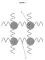
- Some problems are however observed with the state-of-the-art microneedle manufacturing processes. For instance, in the manufacture of out-of-plane microneedles, the yield is limited by the difference of silicon etch rate between the centre and the border of the wafer. Because of this difference some microneedle hats (generally at the periphery of the wafer) fall before the end of the process. The consequence is that the microneedles underneath are no longer protected and as a consequence no longer etched in a controlled manner. Problems therefore arise, in particular microneedle malformation and low production yields.
- microneedle manufacturing process which is characterized by the creation of bridges which link the hats between each others as well as between hats and edges during the manufacturing process.
- the bridges are totally removed at the end of the manufacturing process and result in no modification of the microneedle design.
- the bridges are preferably made of suspended structures. They have a design which is compatible with the materials of the suspended structures and the microneedle fabrication process.
- each bridge may have many different designs. In one embodiment they are rectilinear. In another embodiment they comprise a curved portion.
- each bridge consists of a combination of rectilinear segments and of circle portions, e.g. of 1 ⁇ 2 and 1 ⁇ 4 circles.
- the bridge dimensions can vary depending on the distance between the microneedles as well as the distance between the microneedles and the edge of the wafer.
- the thickness of the bridges which is linked to the thickness of the hats can vary between 100nm and 100um:
- the width of the bridges can vary between 1 um and 100um.
- the material used must have the appropriate characteristics to support the manufacturing process. For example, for a process requiring an excellent conductivity, metal would be chosen. Multilayered bridges, in particular with three layers, offer an interesting compromise when different properties are required as for example good conductivity, high selectivity and mechanical resistance to deformation.
- MEMS microneedle fabrication process as described in Fig. 1 usually starts with a wafer, preferably a silicon wafer 4. On top of this silicon wafer a silicon dioxide layer is used as a protective mask to pattern the microneedles.
- This structuration of the microneedles is performed by a sequence of isotropic and anisotropic etches as represented in Fig 1 steps B to E.
- the first isotropic etch as represented in Fig 1 step B initiates the tip of the microneedle.
- the first anisotropic etch ( Fig. 1 , step C) is used to define the head of the microneedle.
- the goal of the second isotropic etch as represented in Fig 1 step D is to initiate the shoulder of the microneedle and to separate the head of the microneedle with the shaft which is obtain thanks to the second anisotropic etch ( Fig.1 , step E). Finally comes the last isotropic etch ( Fig. 1 , step F) which is the most important etch of the process. Thanks to this etch, we pattern the tip of the microneedle, the backside trough holes and the final design of the microneedle, An oxidation and a silicon oxide etch as represented in Fig.1 , step G are then realized to remove the hats and to polish the silicon surface.
- the present invention provides a way to hold the hats together so that they won't fall before the end of the process. To this effect the hats are linked together and are linked to the edges as displayed in Fig 3 . These links ( Fig. 2 , Ref 3), also named bridges in the present text, will stay in place up to the end of the process and guarantee the stability of each hat until the microneedle fabrication is ended ( Fig.2 Step F). When the process has been completed ( Fig.1 step G) the hat and their links are removed revealing perfect microneedles pattern (see e.g. Fig. 11 ) and chip surface state.
- bridges and hats are deeply linked together; as a matter of fact their are made of same materials and have the same thickness.
- Curved segments as in Fig. 6 and Fig. 7 or combination of rectilinear and curved segments as in Fig. 8 are also possible.
- Multilayered bridges improve the characteristics of the bridges ( Fig. 10 ).
- the metal layers improve the thermal conductivity of the bridges and the non conductive layers improve the mechanical resistance and the high selectivity of the bridges.
Landscapes
- Engineering & Computer Science (AREA)
- Health & Medical Sciences (AREA)
- Manufacturing & Machinery (AREA)
- Life Sciences & Earth Sciences (AREA)
- General Health & Medical Sciences (AREA)
- Biomedical Technology (AREA)
- Heart & Thoracic Surgery (AREA)
- Hematology (AREA)
- Medical Informatics (AREA)
- Animal Behavior & Ethology (AREA)
- Anesthesiology (AREA)
- Public Health (AREA)
- Veterinary Medicine (AREA)
- Dermatology (AREA)
- Analytical Chemistry (AREA)
- Chemical & Material Sciences (AREA)
- Microelectronics & Electronic Packaging (AREA)
- Micromachines (AREA)
Priority Applications (7)
| Application Number | Priority Date | Filing Date | Title |
|---|---|---|---|
| EP07123416A EP2072076A1 (en) | 2007-12-17 | 2007-12-17 | Out-of-plane microneedle manufacturing process |
| EP08862067.9A EP2224993B1 (en) | 2007-12-17 | 2008-10-17 | Out-of-plane microneedle manufacturing process |
| JP2010538958A JP5351173B2 (ja) | 2007-12-17 | 2008-10-17 | 面外極微針の製造方法 |
| PCT/IB2008/054280 WO2009077892A1 (en) | 2007-12-17 | 2008-10-17 | Out-of-plane microneedle manufacturing process |
| US12/808,334 US8999177B2 (en) | 2007-12-17 | 2008-10-17 | Out-of plane microneedle manufacturing process |
| US13/507,368 US9266718B2 (en) | 2007-12-17 | 2012-06-22 | Out-of-plane microneedle manufacturing process |
| US14/988,769 US9561356B2 (en) | 2007-12-17 | 2016-01-06 | Microneedle manufacturing process with hats |
Applications Claiming Priority (1)
| Application Number | Priority Date | Filing Date | Title |
|---|---|---|---|
| EP07123416A EP2072076A1 (en) | 2007-12-17 | 2007-12-17 | Out-of-plane microneedle manufacturing process |
Publications (1)
| Publication Number | Publication Date |
|---|---|
| EP2072076A1 true EP2072076A1 (en) | 2009-06-24 |
Family
ID=39340106
Family Applications (2)
| Application Number | Title | Priority Date | Filing Date |
|---|---|---|---|
| EP07123416A Withdrawn EP2072076A1 (en) | 2007-12-17 | 2007-12-17 | Out-of-plane microneedle manufacturing process |
| EP08862067.9A Not-in-force EP2224993B1 (en) | 2007-12-17 | 2008-10-17 | Out-of-plane microneedle manufacturing process |
Family Applications After (1)
| Application Number | Title | Priority Date | Filing Date |
|---|---|---|---|
| EP08862067.9A Not-in-force EP2224993B1 (en) | 2007-12-17 | 2008-10-17 | Out-of-plane microneedle manufacturing process |
Country Status (4)
| Country | Link |
|---|---|
| US (3) | US8999177B2 (enExample) |
| EP (2) | EP2072076A1 (enExample) |
| JP (1) | JP5351173B2 (enExample) |
| WO (1) | WO2009077892A1 (enExample) |
Families Citing this family (9)
| Publication number | Priority date | Publication date | Assignee | Title |
|---|---|---|---|---|
| EP2072076A1 (en) * | 2007-12-17 | 2009-06-24 | Debiotech S.A. | Out-of-plane microneedle manufacturing process |
| US9649436B2 (en) | 2011-09-21 | 2017-05-16 | Bayer Healthcare Llc | Assembly method for a fluid pump device for a continuous multi-fluid delivery system |
| JP2017536692A (ja) * | 2014-10-31 | 2017-12-07 | ビーコ プリジション サーフェイス プロセシング エルエルシー | ウェット・エッチング・プロセスを実行するための装置および方法 |
| ES3030489T3 (en) | 2015-01-09 | 2025-06-30 | Bayer Healthcare Llc | Multiple fluid delivery system with multi-use disposable set and features thereof |
| GB201709668D0 (en) * | 2017-06-16 | 2017-08-02 | Spts Technologies Ltd | Microneedles |
| JP6519632B2 (ja) * | 2017-11-06 | 2019-05-29 | 大日本印刷株式会社 | マイクロニードルデバイス |
| CN111228643A (zh) * | 2020-02-12 | 2020-06-05 | 成都工业学院 | 一种空心微针阵列装置及其制作方法 |
| CN111228642A (zh) * | 2020-02-12 | 2020-06-05 | 成都工业学院 | 一种中空微针阵列装置及制作方法 |
| JP7438529B2 (ja) * | 2020-03-05 | 2024-02-27 | サムコ株式会社 | 上部にテーパ形状を持つ、深堀構造を有するシリコン基板の製造方法 |
Citations (4)
| Publication number | Priority date | Publication date | Assignee | Title |
|---|---|---|---|---|
| EP0597302A2 (en) * | 1992-10-23 | 1994-05-18 | RICOH SEIKI COMPANY, Ltd. | Etching method for silicon substrate |
| WO2003015860A1 (en) * | 2001-08-14 | 2003-02-27 | Bonsens Ab | Micro needeles and method of manufacture thereof |
| EP1669100A1 (en) * | 2004-12-13 | 2006-06-14 | Debiotech S.A. | Micro-needle |
| WO2008003564A1 (de) * | 2006-07-07 | 2008-01-10 | Robert Bosch Gmbh | Verfahren zur herstellung von mikronadeln in einem si-halbleitersubstrat |
Family Cites Families (3)
| Publication number | Priority date | Publication date | Assignee | Title |
|---|---|---|---|---|
| JP4414774B2 (ja) * | 2004-01-16 | 2010-02-10 | 大日本印刷株式会社 | シリコン針の製造方法 |
| TW200829215A (en) * | 2007-01-03 | 2008-07-16 | Univ Nat Chiao Tung | Micro probe array and manufacturing method of the trans-print mold thereof |
| EP2072076A1 (en) * | 2007-12-17 | 2009-06-24 | Debiotech S.A. | Out-of-plane microneedle manufacturing process |
-
2007
- 2007-12-17 EP EP07123416A patent/EP2072076A1/en not_active Withdrawn
-
2008
- 2008-10-17 JP JP2010538958A patent/JP5351173B2/ja not_active Expired - Fee Related
- 2008-10-17 US US12/808,334 patent/US8999177B2/en not_active Expired - Fee Related
- 2008-10-17 EP EP08862067.9A patent/EP2224993B1/en not_active Not-in-force
- 2008-10-17 WO PCT/IB2008/054280 patent/WO2009077892A1/en not_active Ceased
-
2012
- 2012-06-22 US US13/507,368 patent/US9266718B2/en not_active Expired - Fee Related
-
2016
- 2016-01-06 US US14/988,769 patent/US9561356B2/en not_active Expired - Fee Related
Patent Citations (4)
| Publication number | Priority date | Publication date | Assignee | Title |
|---|---|---|---|---|
| EP0597302A2 (en) * | 1992-10-23 | 1994-05-18 | RICOH SEIKI COMPANY, Ltd. | Etching method for silicon substrate |
| WO2003015860A1 (en) * | 2001-08-14 | 2003-02-27 | Bonsens Ab | Micro needeles and method of manufacture thereof |
| EP1669100A1 (en) * | 2004-12-13 | 2006-06-14 | Debiotech S.A. | Micro-needle |
| WO2008003564A1 (de) * | 2006-07-07 | 2008-01-10 | Robert Bosch Gmbh | Verfahren zur herstellung von mikronadeln in einem si-halbleitersubstrat |
Non-Patent Citations (1)
| Title |
|---|
| LANG W: "Silicon microstructuring technology", MATERIALS SCIENCE AND ENGINEERING R: REPORTS, ELSEVIER SEQUOIA S.A., LAUSANNE, CH, vol. 17, no. 1, 1 September 1996 (1996-09-01), pages 1 - 55, XP004013096, ISSN: 0927-796X * |
Also Published As
| Publication number | Publication date |
|---|---|
| JP5351173B2 (ja) | 2013-11-27 |
| EP2224993A1 (en) | 2010-09-08 |
| JP2011508619A (ja) | 2011-03-17 |
| WO2009077892A1 (en) | 2009-06-25 |
| US20160129232A1 (en) | 2016-05-12 |
| US20100280458A1 (en) | 2010-11-04 |
| EP2224993B1 (en) | 2019-10-16 |
| US9266718B2 (en) | 2016-02-23 |
| US9561356B2 (en) | 2017-02-07 |
| US8999177B2 (en) | 2015-04-07 |
| US20120328835A1 (en) | 2012-12-27 |
Similar Documents
| Publication | Publication Date | Title |
|---|---|---|
| US9266718B2 (en) | Out-of-plane microneedle manufacturing process | |
| TWI380456B (en) | Micro-electro-mechanical device and method for making same | |
| US20090090693A1 (en) | Method for fabricating micromachined structures | |
| JP7519420B2 (ja) | Memsデバイスの構造パラメータを操作する為のmemsグリッド | |
| JP2006189431A (ja) | マイクロファクトリー・コーム容量加速度計 | |
| US20040159629A1 (en) | MEM device processing with multiple material sacrificial layers | |
| US20020195417A1 (en) | Wet and dry etching process on <110> silicon and resulting structures | |
| EP3144271B1 (en) | Unit anodic oxide film structure | |
| JP2018531158A6 (ja) | Memsデバイスの構造パラメータを操作する為のmemsグリッド | |
| JP2012135819A (ja) | Memsデバイス | |
| JP5695741B2 (ja) | 静電容量型圧力センサ及びその製造方法 | |
| TW202238845A (zh) | 具有凹坑特徵及改善的面外靜摩擦之感測器 | |
| JP5649479B2 (ja) | インプリントモールドの製造方法、インプリントモールド、及び配線板 | |
| US9174835B2 (en) | Microstructure and electronic device | |
| US9024408B2 (en) | Double side wafer process, method and device | |
| US9382113B2 (en) | Method for fabricating a self-aligned vertical comb drive structure | |
| KR102237679B1 (ko) | 브릿지형 구조물의 제조 방법 및 이를 이용한 브릿지형 압저항체를 가지는 압저항 가속도 센서의 제조 방법 | |
| TW480621B (en) | Method for producing high density chip | |
| CN101279714A (zh) | 一种微针的制作方法 | |
| US20150191350A1 (en) | Method for the prevention of suspended silicon structure etching during reactive ion etching | |
| JP2012030475A (ja) | インプリントモールドの製造方法 | |
| CN101104508A (zh) | 形成微机电结构的方法及用于制作微机电结构的模具 | |
| JP5634781B2 (ja) | インプリントモールドの製造方法 | |
| TWI483892B (zh) | 微機電裝置以及製造微機電裝置之方法 | |
| KR100921433B1 (ko) | 전해도금을 이용한 경사진 바닥 전극을 갖는 마이크로미러 제작 방법 |
Legal Events
| Date | Code | Title | Description |
|---|---|---|---|
| PUAI | Public reference made under article 153(3) epc to a published international application that has entered the european phase |
Free format text: ORIGINAL CODE: 0009012 |
|
| AK | Designated contracting states |
Kind code of ref document: A1 Designated state(s): AT BE BG CH CY CZ DE DK EE ES FI FR GB GR HU IE IS IT LI LT LU LV MC MT NL PL PT RO SE SI SK TR |
|
| AX | Request for extension of the european patent |
Extension state: AL BA HR MK RS |
|
| AKX | Designation fees paid | ||
| REG | Reference to a national code |
Ref country code: DE Ref legal event code: 8566 |
|
| STAA | Information on the status of an ep patent application or granted ep patent |
Free format text: STATUS: THE APPLICATION IS DEEMED TO BE WITHDRAWN |
|
| 18D | Application deemed to be withdrawn |
Effective date: 20091229 |