EP2063502B1 - Lamp socket, backlight assembly and display device having the same - Google Patents
Lamp socket, backlight assembly and display device having the same Download PDFInfo
- Publication number
- EP2063502B1 EP2063502B1 EP08018543.2A EP08018543A EP2063502B1 EP 2063502 B1 EP2063502 B1 EP 2063502B1 EP 08018543 A EP08018543 A EP 08018543A EP 2063502 B1 EP2063502 B1 EP 2063502B1
- Authority
- EP
- European Patent Office
- Prior art keywords
- lamp
- connection terminal
- inverter
- terminal
- socket
- Prior art date
- Legal status (The legal status is an assumption and is not a legal conclusion. Google has not performed a legal analysis and makes no representation as to the accuracy of the status listed.)
- Not-in-force
Links
Images



Classifications
-
- G—PHYSICS
- G02—OPTICS
- G02F—OPTICAL DEVICES OR ARRANGEMENTS FOR THE CONTROL OF LIGHT BY MODIFICATION OF THE OPTICAL PROPERTIES OF THE MEDIA OF THE ELEMENTS INVOLVED THEREIN; NON-LINEAR OPTICS; FREQUENCY-CHANGING OF LIGHT; OPTICAL LOGIC ELEMENTS; OPTICAL ANALOGUE/DIGITAL CONVERTERS
- G02F1/00—Devices or arrangements for the control of the intensity, colour, phase, polarisation or direction of light arriving from an independent light source, e.g. switching, gating or modulating; Non-linear optics
- G02F1/01—Devices or arrangements for the control of the intensity, colour, phase, polarisation or direction of light arriving from an independent light source, e.g. switching, gating or modulating; Non-linear optics for the control of the intensity, phase, polarisation or colour
- G02F1/13—Devices or arrangements for the control of the intensity, colour, phase, polarisation or direction of light arriving from an independent light source, e.g. switching, gating or modulating; Non-linear optics for the control of the intensity, phase, polarisation or colour based on liquid crystals, e.g. single liquid crystal display cells
- G02F1/133—Constructional arrangements; Operation of liquid crystal cells; Circuit arrangements
- G02F1/1333—Constructional arrangements; Manufacturing methods
- G02F1/1335—Structural association of cells with optical devices, e.g. polarisers or reflectors
-
- G—PHYSICS
- G02—OPTICS
- G02F—OPTICAL DEVICES OR ARRANGEMENTS FOR THE CONTROL OF LIGHT BY MODIFICATION OF THE OPTICAL PROPERTIES OF THE MEDIA OF THE ELEMENTS INVOLVED THEREIN; NON-LINEAR OPTICS; FREQUENCY-CHANGING OF LIGHT; OPTICAL LOGIC ELEMENTS; OPTICAL ANALOGUE/DIGITAL CONVERTERS
- G02F1/00—Devices or arrangements for the control of the intensity, colour, phase, polarisation or direction of light arriving from an independent light source, e.g. switching, gating or modulating; Non-linear optics
- G02F1/01—Devices or arrangements for the control of the intensity, colour, phase, polarisation or direction of light arriving from an independent light source, e.g. switching, gating or modulating; Non-linear optics for the control of the intensity, phase, polarisation or colour
- G02F1/13—Devices or arrangements for the control of the intensity, colour, phase, polarisation or direction of light arriving from an independent light source, e.g. switching, gating or modulating; Non-linear optics for the control of the intensity, phase, polarisation or colour based on liquid crystals, e.g. single liquid crystal display cells
- G02F1/133—Constructional arrangements; Operation of liquid crystal cells; Circuit arrangements
- G02F1/1333—Constructional arrangements; Manufacturing methods
- G02F1/1335—Structural association of cells with optical devices, e.g. polarisers or reflectors
- G02F1/1336—Illuminating devices
- G02F1/133602—Direct backlight
- G02F1/133604—Direct backlight with lamps
-
- G—PHYSICS
- G02—OPTICS
- G02F—OPTICAL DEVICES OR ARRANGEMENTS FOR THE CONTROL OF LIGHT BY MODIFICATION OF THE OPTICAL PROPERTIES OF THE MEDIA OF THE ELEMENTS INVOLVED THEREIN; NON-LINEAR OPTICS; FREQUENCY-CHANGING OF LIGHT; OPTICAL LOGIC ELEMENTS; OPTICAL ANALOGUE/DIGITAL CONVERTERS
- G02F1/00—Devices or arrangements for the control of the intensity, colour, phase, polarisation or direction of light arriving from an independent light source, e.g. switching, gating or modulating; Non-linear optics
- G02F1/01—Devices or arrangements for the control of the intensity, colour, phase, polarisation or direction of light arriving from an independent light source, e.g. switching, gating or modulating; Non-linear optics for the control of the intensity, phase, polarisation or colour
- G02F1/13—Devices or arrangements for the control of the intensity, colour, phase, polarisation or direction of light arriving from an independent light source, e.g. switching, gating or modulating; Non-linear optics for the control of the intensity, phase, polarisation or colour based on liquid crystals, e.g. single liquid crystal display cells
- G02F1/133—Constructional arrangements; Operation of liquid crystal cells; Circuit arrangements
- G02F1/1333—Constructional arrangements; Manufacturing methods
- G02F1/1335—Structural association of cells with optical devices, e.g. polarisers or reflectors
- G02F1/1336—Illuminating devices
- G02F1/133602—Direct backlight
- G02F1/133608—Direct backlight including particular frames or supporting means
-
- H—ELECTRICITY
- H01—ELECTRIC ELEMENTS
- H01R—ELECTRICALLY-CONDUCTIVE CONNECTIONS; STRUCTURAL ASSOCIATIONS OF A PLURALITY OF MUTUALLY-INSULATED ELECTRICAL CONNECTING ELEMENTS; COUPLING DEVICES; CURRENT COLLECTORS
- H01R33/00—Coupling devices specially adapted for supporting apparatus and having one part acting as a holder providing support and electrical connection via a counterpart which is structurally associated with the apparatus, e.g. lamp holders; Separate parts thereof
- H01R33/02—Single-pole devices, e.g. holder for supporting one end of a tubular incandescent or neon lamp
-
- H—ELECTRICITY
- H01—ELECTRIC ELEMENTS
- H01R—ELECTRICALLY-CONDUCTIVE CONNECTIONS; STRUCTURAL ASSOCIATIONS OF A PLURALITY OF MUTUALLY-INSULATED ELECTRICAL CONNECTING ELEMENTS; COUPLING DEVICES; CURRENT COLLECTORS
- H01R33/00—Coupling devices specially adapted for supporting apparatus and having one part acting as a holder providing support and electrical connection via a counterpart which is structurally associated with the apparatus, e.g. lamp holders; Separate parts thereof
- H01R33/05—Two-pole devices
- H01R33/06—Two-pole devices with two current-carrying pins, blades or analogous contacts, having their axes parallel to each other
- H01R33/08—Two-pole devices with two current-carrying pins, blades or analogous contacts, having their axes parallel to each other for supporting tubular fluorescent lamp
-
- H—ELECTRICITY
- H01—ELECTRIC ELEMENTS
- H01R—ELECTRICALLY-CONDUCTIVE CONNECTIONS; STRUCTURAL ASSOCIATIONS OF A PLURALITY OF MUTUALLY-INSULATED ELECTRICAL CONNECTING ELEMENTS; COUPLING DEVICES; CURRENT COLLECTORS
- H01R4/00—Electrically-conductive connections between two or more conductive members in direct contact, i.e. touching one another; Means for effecting or maintaining such contact; Electrically-conductive connections having two or more spaced connecting locations for conductors and using contact members penetrating insulation
- H01R4/28—Clamped connections, spring connections
- H01R4/48—Clamped connections, spring connections utilising a spring, clip, or other resilient member
- H01R4/4809—Clamped connections, spring connections utilising a spring, clip, or other resilient member using a leaf spring to bias the conductor toward the busbar
- H01R4/48185—Clamped connections, spring connections utilising a spring, clip, or other resilient member using a leaf spring to bias the conductor toward the busbar adapted for axial insertion of a wire end
- H01R4/4819—Clamped connections, spring connections utilising a spring, clip, or other resilient member using a leaf spring to bias the conductor toward the busbar adapted for axial insertion of a wire end the spring shape allowing insertion of the conductor end when the spring is unbiased
- H01R4/4821—Single-blade spring
-
- H—ELECTRICITY
- H01—ELECTRIC ELEMENTS
- H01R—ELECTRICALLY-CONDUCTIVE CONNECTIONS; STRUCTURAL ASSOCIATIONS OF A PLURALITY OF MUTUALLY-INSULATED ELECTRICAL CONNECTING ELEMENTS; COUPLING DEVICES; CURRENT COLLECTORS
- H01R4/00—Electrically-conductive connections between two or more conductive members in direct contact, i.e. touching one another; Means for effecting or maintaining such contact; Electrically-conductive connections having two or more spaced connecting locations for conductors and using contact members penetrating insulation
- H01R4/28—Clamped connections, spring connections
- H01R4/48—Clamped connections, spring connections utilising a spring, clip, or other resilient member
- H01R4/4809—Clamped connections, spring connections utilising a spring, clip, or other resilient member using a leaf spring to bias the conductor toward the busbar
- H01R4/4846—Busbar details
- H01R4/4848—Busbar integrally formed with the spring
Definitions
- the present invention relates to a lamp socket, a backlight assembly and a display device having the same. More particularly, the present invention relates to a lamp socket that can reduce the number of constituent elements and the thickness of both sides of a display panel, and a backlight assembly and a display device having the same.
- a backlight assembly adopted in a liquid crystal display is classified into a direct downward type backlight assembly and an edge type backlight assembly in accordance with the arrangement of a light source.
- a representative light source for use in a backlight assembly is a cold cathode fluorescent lamp ("CCFL").
- CCFL cold cathode fluorescent lamp
- a direct downward type backlight assembly adopting CCFLs may include lamp sockets for fixing the lamps to a bottom plate of a receptacle.
- a backlight assembly having lamp sockets into which electrode parts of the lamps are inserted has been developed.
- a conventional lamp socket necessarily has a specified thickness, and thus the thickness of both sides of a display panel is increased.
- a lamp socket that has a pair of opposed torsion blades that are twisted towards each other and that provides double torsion contact action when a contact pin of a bi-pin fluorescent lamp is inserted therein for reliably maintaining the contact pin between the plates.
- An electrical socket for the lamp is provided having a pair of contact chambers and a double torsion blade connector mounted to each chamber.
- the electrical socket includes a housing that comprises a wire receiving section having a pair of contact locking recesses. Each of the recesses includes a pair of conductor receiving passageways that extending trough the front wall.
- a plurality lamp sockets and inverters are soldered through wires, or terminals of a plurality of lamp sockets and inverters are soldered US 2007/230169 A1 describes a backlight assembly employing a plurality of lamp sockets, each of which employs two parallel located power terminals separated by a slit. The two power terminals move apart when the pin of a lamp is inserted, whereupon electric contact is made and at the same time pressure forces are applied to the pin holding the lamp in place.
- Document JP H 0730481 U discloses a socket comprising a guide groove into which an electrode is inserted, and a plate spring arranged on one side of the groove to press the electrode.
- the increased thickness of the panel due to the conventional lamp socket is an obstacle to diverse shapes of a display device, and causes low compatibility and inferior external appearance of the display device.
- the present invention provides a lamp socket according to claim 1 that can reduce the thickness of both sides of a display panel.
- the present invention also provides a backlight assembly that includes the lamp sockets according to claim 1 and reduces the thickness of both sides of a display panel.
- the present invention also provides a display device that includes the lamp sockets according to claim 1.
- a lamp socket includes a socket main body having a contact hole formed therein, and a power-applying member coupled to the socket main body through the contact hole, and provided with a lamp connection terminal, an inverter connection terminal, and a terminal connection part connected to the lamp connection terminal in a bent form so as to connect the lamp connection terminal with the inverter connection terminal.
- a backlight assembly includes a receptacle having a bottom plate on which openings are formed and side walls arranged around the bottom plate, a plurality of lamps having lamp main bodies and electrode parts formed at edges of the lamp main bodies, respectively, and arranged on the bottom plate, a plurality of lamp sockets each including a socket main body having a contact hole formed therein, and a power-applying member coupled to the socket main body through the contact hole and provided with a lamp connection terminal, an inverter connection terminal, and a terminal connection part connected to the lamp connection terminal in a bent form so as to connect the lamp connection terminal with the inverter connection terminal, and a power supply board arranged on a rear surface of the bottom plate and outputting a lamp-driving voltage to the power-applying member.
- a display device includes a receptacle having a bottom plate on which openings are formed and side walls, a plurality of lamps having lamp main bodies and electrode parts formed at edges of the lamp main bodies, respectively, and arranged on the bottom plate, a plurality of lamp sockets each including a socket main body having a contact hole formed therein, and a power-applying member coupled to the socket main body through the contact hole and provided with a lamp connection terminal, an inverter connection terminal, and a terminal connection part connected with the lamp connection terminal in a bent form so as to connect the lamp connection terminal with the inverter connection terminal, a power supply board having one side edge inserted into an inverter insertion hole and applying a lamp driving voltage to the inverter connection terminal, a side cover covering the socket main bodies, optical sheets supported by the side cover, and a display panel arranged on the optical sheets.
- first, second, third etc. may be used herein to describe various elements, components, regions, layers and/or sections, these elements, components, regions, layers and/or sections should not be limited by these terms. These terms are only used to distinguish one element, component, region, layer or section from another element, component, region, layer or section. Thus, a first element, component, region, layer or section discussed below could be termed a second element, component, region, layer or section without departing from the teachings of the present invention.
- spatially relative terms such as “beneath”, “below”, “lower”, “above”, “upper” and the like, may be used herein for ease of description to describe one element or feature's relationship to another element(s) or feature(s) as illustrated in the figures. It will be understood that the spatially relative terms are intended to encompass different orientations of the device in use or operation in addition to the orientation depicted in the figures. For example, if the device in the figures is turned over, elements described as “below” or “beneath” other elements or features would then be oriented “above” the other elements or features. Thus, the exemplary term “below” can encompass both an orientation of above and below. The device may be otherwise oriented (rotated 90 degrees or at other orientations) and the spatially relative descriptors used herein interpreted accordingly.
- Embodiments of the present invention are described herein with reference to cross section illustrations that are schematic illustrations of idealized embodiments of the present invention. As such, variations from the shapes of the illustrations as a result, for example, of manufacturing techniques and/or tolerances, are to be expected. Thus, embodiments of the present invention should not be construed as limited to the particular shapes of regions illustrated herein but are to include deviations in shapes that result, for example, from manufacturing. For example, a region illustrated or described as flat may, typically, have rough and/or nonlinear features. Moreover, sharp angles that are illustrated may be rounded. Thus, the regions illustrated in the figures are schematic in nature and their shapes are not intended to illustrate the precise shape of a region and are not intended to limit the scope of the present invention.
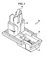
- FIG. 1 is a perspective view of an exemplary lamp socket according to an exemplary embodiment of the present invention
- FIG. 2 is a side view of the exemplary lamp socket illustrated in FIG. 1
- FIG. 3 is a perspective view of the exemplary power-applying member illustrated in FIGS. 1 and 2 .
- a lamp socket 20 includes a socket main body 30 and a power-applying member 40.
- the lamp socket 20 fixes lamps, for providing rear light in a display device, to a receptacle, and applies a lamp driving voltage to the lamps.
- the socket main body 30 is a three-dimensional molded product, and a contact hole 35 is formed on an upper part of the socket main body 30.
- a contact hole 35 is formed on an upper part of the socket main body 30.
- an inverter insertion hole 31 that is connected to the contact hole 35 is formed.
- the inverter insertion hole 31 is formed on the lower part of the socket main body 30, and the contact hole 35 is open toward an upper surface of the socket main body 30.
- the contact hole 35 may extend is a different direction than a direction in which the inverter insertion hole 31 extends.
- the contact hole 35 may extend in a direction that is substantially perpendicular to an extending direction of the inverter insertion hole 31.
- the power-applying member 40 is coupled to the socket main body 30 through the contact hole 35.
- the power-applying member 40 is made of conductive metal, and electrically connects electrode parts of the inverter and the lamp with each other.
- the power-applying member 40 includes a lamp connection terminal 44, an inverter connection terminal 45, and a terminal connection part 46 connecting the lamp connection terminal 44 with the inverter connection terminal 45.
- the terminal connection part 46, the lamp connection terminal 44, and the inverter connection terminal 45 may be formed in a body. In other words, the terminal connection part 46, the lamp connection terminal 44, and the inverter connection terminal 45 may be integrally formed in a unitary piece.
- the terminal connection part 46 has at least one bent part, and thus may be connected to the lamp connection terminal 44 and the inverter connection terminal 45 in a bent form.
- the terminal connection part 46 may be composed of at least one horizontal portion and at least one vertical portion.
- the lamp connection terminal 44 is not required to be arranged on the same vertical line as the inverter connection terminal 45. Accordingly, if the lamp connection terminal 44 is arranged on a side part of the display device, the inverter connection terminal 45 can be relatively arranged on a center part of the display device, and thus the thickness of both side parts of the display device can be reduced. Thus, the compatibility of the display device can be increased, and the display device can be slimmed.
- the terminal connection part 46 may have diverse shapes, and may be provided with two or more bent parts to connect the lamp connection terminal 44 with the inverter connection terminal 45. In addition, the terminal connection part 46 may be in the form of steps.
- the lamp connection terminal 44 is exposed to the outside through the contact hole 35, and the inverter connection terminal 45 is exposed to an outside through the inverter insertion hole 31.
- the lamp connection terminal 44 may extend generally in the direction that the contact hole 35 extends and the inverter connection terminal 45 may extend generally in the direction that the inverter insertion hole 31 extends, and the terminal connection part 46 has the above-described configuration such that a connection between the lamp connection terminal 44 and the inverter connection terminal 45 extending in different directions is made possible.
- the lamp connection terminal 44 may include a first plate 41, a first guide groove 42, and a plate spring 43.
- two first plates 41 are arranged side by side, and each side part of the pair of the first plates 41 is connected.
- Two first plates 41 may be arranged substantially parallel to each other and spaced apart by a distance, which may be equivalent to a width of a side connecting strip connecting the side parts or edges of the two first plates 41 together.
- the first guide groove 42, into which the lamp is inserted, is formed on at least the first plate 41 positioned closer to the lamp, although the first guide groove 42 may be formed on both the first plates 41.
- the plate spring 43 is arranged on one side of the first plate 41 that pressingly fixes the lamp inserted into the first guide groove 42.
- the plate spring 43 may be formed in a body with connection parts of the pair of first plates 41.
- the width of the side connecting strip may be at least as great or greater than a width of the plate spring 43, and the plate spring 43 may extend upwardly from a top portion of the side connecting strip and may then be bent downwardly so as to be positioned between the first plates 41.
- the plate spring 43 may then be disposed at an angle such that it is positioned adjacent to the first guide groove 42.
- the lamp socket 20 according to an embodiment of the present invention has a structure from which a socket cover can be excluded, and the lamp can be fixed to the lamp connection terminal 44 of the power-applying member 40 using the first guide groove 42 and the plate spring 43.
- the electrode of the lamp is introduced between the plate spring 43 and the first guide groove 42 by an external force.
- the plate spring 43 may include a recessed surface to facilitate the introduction of the electrode of the lamp.
- the first guide groove 42 may include a slot that extends in the extending direction of the contact hole 35, and may include an indentation extending from the bottom of the slot, in a different direction from the extending direction, to receive the electrode of the lamp therein.
- the electrode may be retained within the indentation of the first guide groove 42 by the recessed surface of the plate spring 43.
- connection portion may depend from the inverter connection terminal 45 such that the connection portion may secure the power applying member 40 to the socket main body 30.
- the connection portion may include prongs as shown in FIG. 3 which may be inserted within an opening in the socket main body 30.
- the lamp socket 20 may further include a socket cover (not illustrated).
- a socket cover (not illustrated).
- a lead wire of the lamp is fixed to the lamp socket 20 in a manner that the power-applying member 40 is inserted into a hole formed on the socket main body 30, the lead wire of the lamp is fitted into the terminal of the power-applying member 40, and then the socket cover is inserted into the socket main body 30.
- FIG. 4 is a perspective view of an exemplary power-applying module according to an exemplary embodiment of the present invention
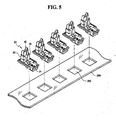
- FIG. 5 is an exploded perspective view of the exemplary power-applying module illustrated in FIG. 4 .
- a power-applying module 200 includes a plurality of lamp sockets 20 that can be coupled to a plurality of lamps, and a connection plate 260 onto which the plurality of lamp sockets 20 are inserted and arranged.
- connection plate 260 is in the form of a plate elongated in one direction.
- the connection plate 260 may be extended in a direction that is substantially perpendicular to an extending direction of the contact hole 35 and substantially perpendicular to an extending direction of the inverter insertion hole 31.
- a plurality of socket fixing parts 265 are formed at predetermined intervals. That is, the socket fixing parts 265 may be substantially evenly spaced apart from each other.
- the socket fixing part 265 may be an opening formed on the connection plate 260.
- the lamp socket 20 composed of the power-applying member 40 and the socket main body 30 may be inserted into and fixed to the socket fixing part 265.
- the inverter insertion hole 31 formed on the socket main body 30 is exposed to a lower part of the connection plate 260.
- the contact hole 35 formed on the socket main body 30 is exposed to an upper part of the connection plate 260.
- the connection plate 260 may include an upper surface and an opposing lower surface, and the contact hole 35 is available above the upper surface of the connection plate 260 and the inverter insertion hole 31 is available below the lower surface of the connection plate 260.
- the power-applying module may be in a form (not illustrated) in which a plurality of lamp sockets is formed in a body without using any separate connection plate.
- a socket main body may have a plurality of contact holes and a plurality of inverter insertion holes and may be integrally formed with a plate that spaces the contact holes at a distance and the insertion holes at a distance for receiving the lamps and inverters, respectively.
- FIG. 6 is an exploded perspective view of an exemplary backlight assembly according to an exemplary embodiment of the present invention
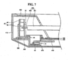
- FIG. 7 is a sectional view of the exemplary backlight assembly taken along line VII-VII' of FIG. 6 .
- a backlight assembly 400 includes a receptacle 410, a plurality of lamp sockets 20, a plurality of lamps 450, and a power supply board 470.
- the receptacle 410 includes a bottom plate 405, and first to fourth side walls 411, 413, 415, and 417 arranged around the bottom plate 405.
- the first and second side walls 411 and 413 are arranged on opposite sides of the receptacle 410 to face each other.
- the third and fourth side walls 415 and 417 are arranged on opposite sides of the receptacle 410 to face each other, and are connected to the first and second side walls 411 and 413, respectively.
- stepped portions are formed on the bottom plate 405 neighboring the first and second side walls 411 and 413.
- the lamp 450 includes a lamp main body 451 and an electrode part 455.
- the lamp main body 451 is in the form of a straight tube, and a discharge gas such as argon or mercury (Hg) is injected into the lamp main body 451.
- the electrode part 455 is arranged at an edge of the lamp main body 451.
- the electrode part 455 includes a discharge electrode and a lead wire.
- the discharge electrode is positioned inside the lamp main body 451, and the lead wire extends from the discharge electrode to an outside of the lamp main body 451.
- the lead wire of the electrode part 455 is inserted into the slot of the first guide groove 42 while pressure is placed by the lead wire on the plate spring 43, and then the lead wire enters the indentation of the first guide groove 42.
- the plate spring 43 presses the lead wire into place within the indentation, thus retaining the lamp 450 into position with respect to the lamp socket 20 and ensuring contact between the lead wire of the lamp 450 and the lamp connection terminal 44 of the power applying member 40.
- the lamp 450 may be an external electrode fluorescent lamp ("EEFL").
- the lamp socket 20 is inserted into the opening of the socket fixing part 265 formed on the connection plate 260.
- the connection plate 260 is arranged near each of the first and second side walls 411 and 413.
- the plurality of lamp sockets 20, inserted into the connection plate 260 is respectively inserted into the plurality of openings 407 formed on the bottom plate 405.
- the connection plate 260 may then lie substantially flush with the bottom plate 405. In this case, the inverter insertion hole 31 is exposed to the rear surface of the bottom plate 405, and the contact hole 35 is exposed to an inside of the receptacle 410.
- the backlight assembly 400 may further include a reflecting plate 409.
- the reflecting plate 409 is arranged on the bottom plate 405 of the receptacle 410, and reflects light emitted from the lamps 450 to an upper part of the backlight assembly 400.
- the power supply board 470 is arranged on the rear surface of the bottom plate 405, and outputs a lamp driving voltage.
- the power supply board 470 may include a printed circuit board (“PCB”) and a power supply element mounted on the PCB,
- One edge of the power supply board 470 is inserted into the inverter insertion hole 31 of the lamp socket 20.
- One edge part of the power supply board 470 that corresponds to the inverter insertion hole 31 is projected toward the inverter insertion hole 31.
- the edge of the power supply board 470 is in the form of prominence and depression, wherein the prominence or projection is inserted in the inverter insertion hole 31.
- the inverter connection terminal 45 disposed within the inverter insertion hole 31 may include a spring like portion folded over to form an inverted C-shape such that when the projected part of the power supply board 470 is inserted into the inverter insertion hole 31, the projected part pushes onto the spring like portion of the inverter connection terminal 45 to ensure a connection with the inverter connection terminal 45.
- a power supply terminal is formed.
- the power supply terminal for example, may be an exposed part of the conductive wire formed on the PCB.
- the backlight assembly 400 may further include a case 475 that protects the power supply board 470, and intercepts electromagnetic waves.
- the backlight assembly 400 may further include a side cover 480.
- the side cover 480 covers and protects the lamp sockets 20 arranged on the first and second side walls 411 and 413 in the receptacle 410.
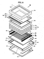
- FIG. 8 is an exploded perspective view of an exemplary display device according to an exemplary embodiment of the present invention
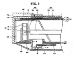
- FIG. 9 is a sectional view of the exemplary display device taken along line IX-IX' of FIG. 8 .
- a display device 600 includes a receptacle 410, a plurality of lamp sockets 20, a plurality of lamps 450, a connection plate 260, a power supply board 470, a side cover 480, optical sheets 710, and a display panel 750.
- the optical sheets 710 improve the optical characteristics of light emitted from the lamps 450 and emit the improved light.
- the optical sheets 710 may include a diffusion plate 711, a diffusion sheet 713, and condensing sheets 715 laminated in order.
- the diffusion plate 711, the diffusion sheet 713, and the condensing sheets 715 are supported by stepped portions formed on the third side wall 415, the fourth side wall 417, and the side cover 480.
- the diffusion plate 711 diffuses the light emitted from the lamps 450 to improve the luminance uniformity.
- the diffusion sheet 713 converts the light randomly diffused by the diffusion plate 711 into the diffused light having a constant diffusion angle.
- the condensing sheets 715 condense the diffused light in different directions, and preferably in directions perpendicular to each other, so that the front luminance of the light emitted by the lamp 450 is improved.
- the display device 600 may further include a middle frame 730.
- the middle frame 730 covers the edges of the optical sheets 710, and is coupled to the receptacle 410.
- the display panel 750 displays an image based on the light emitted from the optical sheets 710.
- the display panel 750 includes a first substrate 751, a second substrate 755 facing the first substrate 751, and a liquid crystal layer interposed between the first substrate 751 and the second substrate 755.
- the display device 600 may further include a PCB 757 and a connection film 758.
- the PCB 757 outputs a panel driving signal to the display panel 750.
- One end portion of the connection film 758 is electrically connected to the edge of the first substrate 751, and the other end portion of the connection film 758 is electrically connected to the PCB 757.
- the display device 600 exposes an effective display region of the display panel 750, and may further include a top chassis 770 coupled to the receptacle 410 or the middle frame 730.
Landscapes
- Physics & Mathematics (AREA)
- Nonlinear Science (AREA)
- Mathematical Physics (AREA)
- Chemical & Material Sciences (AREA)
- Crystallography & Structural Chemistry (AREA)
- General Physics & Mathematics (AREA)
- Optics & Photonics (AREA)
- Planar Illumination Modules (AREA)
- Liquid Crystal (AREA)
- Fastening Of Light Sources Or Lamp Holders (AREA)
- Connecting Device With Holders (AREA)
Applications Claiming Priority (1)
| Application Number | Priority Date | Filing Date | Title |
|---|---|---|---|
| KR1020070119299A KR101385226B1 (ko) | 2007-11-21 | 2007-11-21 | 램프 소켓, 이를 갖는 백라이트 어셈블리 및 표시장치 |
Publications (3)
| Publication Number | Publication Date |
|---|---|
| EP2063502A2 EP2063502A2 (en) | 2009-05-27 |
| EP2063502A3 EP2063502A3 (en) | 2012-06-06 |
| EP2063502B1 true EP2063502B1 (en) | 2015-07-15 |
Family
ID=40456877
Family Applications (1)
| Application Number | Title | Priority Date | Filing Date |
|---|---|---|---|
| EP08018543.2A Not-in-force EP2063502B1 (en) | 2007-11-21 | 2008-10-23 | Lamp socket, backlight assembly and display device having the same |
Country Status (5)
| Country | Link |
|---|---|
| US (1) | US7926965B2 (https=) |
| EP (1) | EP2063502B1 (https=) |
| JP (1) | JP5216410B2 (https=) |
| KR (1) | KR101385226B1 (https=) |
| CN (1) | CN101488633B (https=) |
Families Citing this family (23)
| Publication number | Priority date | Publication date | Assignee | Title |
|---|---|---|---|---|
| CN101681051B (zh) * | 2007-05-17 | 2012-09-05 | 夏普株式会社 | 显示装置用照明装置、显示装置 |
| TWI350931B (en) * | 2007-09-12 | 2011-10-21 | Au Optronics Corp | Backlight structure |
| JP4495229B2 (ja) * | 2008-06-16 | 2010-06-30 | 日本圧着端子製造株式会社 | 電気コネクタの取付構造 |
| KR101322313B1 (ko) * | 2008-06-17 | 2013-10-25 | 엘지디스플레이 주식회사 | 액정표시장치 |
| WO2010004795A1 (ja) * | 2008-07-08 | 2010-01-14 | シャープ株式会社 | 照明装置、及び表示装置 |
| KR20100008184A (ko) * | 2008-07-15 | 2010-01-25 | 삼성전자주식회사 | 램프 소켓, 이를 포함하는 백라이트 어셈블리 및 램프 조립방법 |
| KR101537712B1 (ko) * | 2008-09-19 | 2015-07-20 | 삼성디스플레이 주식회사 | 백라이트 어셈블리 및 이의 조립 방법 |
| KR20100048191A (ko) * | 2008-10-30 | 2010-05-11 | 삼성전자주식회사 | 램프 소켓 어셈블리, 백라이트 어셈블리, 표시 장치 및 표시 장치의 제조 방법 |
| JP5269104B2 (ja) * | 2009-01-27 | 2013-08-21 | シャープ株式会社 | 照明装置、表示装置、及びテレビ受信装置 |
| US20100238621A1 (en) * | 2009-03-20 | 2010-09-23 | Tracy Mark S | Insert-molded conductor |
| TWM370104U (en) * | 2009-05-14 | 2009-12-01 | Chunghwa Picture Tubes Ltd | Backlight component fixing mechanism and related backlight module |
| JP2011081991A (ja) * | 2009-10-06 | 2011-04-21 | Japan Aviation Electronics Industry Ltd | コンタクト及びコネクタ |
| JP5063659B2 (ja) * | 2009-10-20 | 2012-10-31 | 日本航空電子工業株式会社 | コネクタ |
| KR20110058488A (ko) * | 2009-11-26 | 2011-06-01 | 삼성전자주식회사 | 슬림형 lcd모듈 및 이를 위한 소켓 |
| KR20110111029A (ko) * | 2010-04-02 | 2011-10-10 | 삼성전자주식회사 | 램프 소켓, 이를 갖는 백라이트 어셈블리 및 표시장치 |
| CN201927740U (zh) * | 2010-06-14 | 2011-08-10 | 富士康(昆山)电脑接插件有限公司 | 灯管连接器 |
| CN102486669A (zh) * | 2010-12-01 | 2012-06-06 | 鸿富锦精密工业(深圳)有限公司 | 电子装置 |
| US8435060B2 (en) * | 2011-01-03 | 2013-05-07 | Cree, Inc. | Fixtures, apparatuses, and related methods for providing load bearing connections for lighting devices |
| CN102588840A (zh) * | 2012-02-16 | 2012-07-18 | 深圳市华星光电技术有限公司 | 背光模组及液晶显示装置 |
| US8956019B2 (en) * | 2012-08-27 | 2015-02-17 | Ideal Industries, Inc. | Methods and apparatus for grounding an electrical device via a lampholder |
| US10317238B2 (en) | 2014-01-09 | 2019-06-11 | Telenav, Inc. | Navigation system with ranking mechanism and method of operation thereof |
| CN204943397U (zh) * | 2015-07-22 | 2016-01-06 | 厦门广泓工贸有限公司 | Led灯驱动板与灯头电连接端子和电连接器及led灯 |
| TWM529310U (zh) * | 2016-03-11 | 2016-09-21 | Switchlab Inc | 導線聯接端子之接電頭限制器結構 |
Citations (1)
| Publication number | Priority date | Publication date | Assignee | Title |
|---|---|---|---|---|
| JPH0730481U (ja) * | 1993-11-11 | 1995-06-06 | 第一電装部品株式会社 | 挾支接続片 |
Family Cites Families (12)
| Publication number | Priority date | Publication date | Assignee | Title |
|---|---|---|---|---|
| US4863394A (en) * | 1985-05-20 | 1989-09-05 | General Electric Company | Electrical connector with double torsion contacts |
| US4918582A (en) * | 1987-12-16 | 1990-04-17 | F.L. Industries, Inc. | Mating terminal and socket assembly |
| JP3932285B2 (ja) * | 2003-05-06 | 2007-06-20 | 日本航空電子工業株式会社 | ランプ保持構造 |
| KR101068385B1 (ko) * | 2004-09-07 | 2011-09-28 | 엘지디스플레이 주식회사 | 액정표시장치 백라이트 어셈블리 및 전극판 구조 |
| KR20070081261A (ko) | 2006-02-10 | 2007-08-16 | 삼성전자주식회사 | 램프홀더 및 이를 갖는 백라이트 어셈블리 |
| KR20070074168A (ko) * | 2006-01-06 | 2007-07-12 | 삼성전자주식회사 | 전원 공급 유닛, 이를 갖는 백라이트 어셈블리 및 표시장치 |
| KR20070052390A (ko) * | 2005-11-17 | 2007-05-22 | 삼성전자주식회사 | 백라이트 어셈블리 및 이를 갖는 표시장치 |
| KR101255545B1 (ko) * | 2006-01-24 | 2013-04-16 | 삼성디스플레이 주식회사 | 램프 지지 유닛과 이를 포함하는 백라이트 어셈블리 및액정 표시 장치 |
| JP4509054B2 (ja) * | 2006-03-20 | 2010-07-21 | 日本圧着端子製造株式会社 | 複合コネクタ、複合コネクタに用いられるホルダ、回路基板への蛍光管の端子の接続構造、および回路基板への蛍光管の端子の接続方法 |
| KR101294012B1 (ko) * | 2006-04-03 | 2013-08-08 | 삼성디스플레이 주식회사 | 램프홀더, 전원공급모듈, 이를 갖는 백라이트 어셈블리 및표시장치 |
| CN100589292C (zh) * | 2006-04-14 | 2010-02-10 | 日本航空电子工业株式会社 | 连接器装置及使用该装置的背光灯组合体 |
| KR101295074B1 (ko) * | 2006-07-20 | 2013-08-08 | 삼성디스플레이 주식회사 | 백라이트 유닛 및 이를 포함한 액정표시장치 |
-
2007
- 2007-11-21 KR KR1020070119299A patent/KR101385226B1/ko not_active Expired - Fee Related
-
2008
- 2008-05-08 JP JP2008122158A patent/JP5216410B2/ja not_active Expired - Fee Related
- 2008-06-11 US US12/137,033 patent/US7926965B2/en not_active Expired - Fee Related
- 2008-10-23 EP EP08018543.2A patent/EP2063502B1/en not_active Not-in-force
- 2008-10-23 CN CN2008101713829A patent/CN101488633B/zh not_active Expired - Fee Related
Patent Citations (1)
| Publication number | Priority date | Publication date | Assignee | Title |
|---|---|---|---|---|
| JPH0730481U (ja) * | 1993-11-11 | 1995-06-06 | 第一電装部品株式会社 | 挾支接続片 |
Also Published As
| Publication number | Publication date |
|---|---|
| EP2063502A3 (en) | 2012-06-06 |
| JP2009129901A (ja) | 2009-06-11 |
| EP2063502A2 (en) | 2009-05-27 |
| KR101385226B1 (ko) | 2014-04-15 |
| US20090128734A1 (en) | 2009-05-21 |
| CN101488633B (zh) | 2013-04-17 |
| US7926965B2 (en) | 2011-04-19 |
| KR20090052680A (ko) | 2009-05-26 |
| CN101488633A (zh) | 2009-07-22 |
| JP5216410B2 (ja) | 2013-06-19 |
Similar Documents
| Publication | Publication Date | Title |
|---|---|---|
| EP2063502B1 (en) | Lamp socket, backlight assembly and display device having the same | |
| EP1883138B1 (en) | Lamp socket, backlight assembly having the same and display device having the same | |
| US7771106B2 (en) | Lamp socket, backlight assembly having the same, display device having the same and method of assembling a lamp module | |
| US7862191B2 (en) | Lamp socket, backlight assembly having the same, and display device having the same | |
| US20060279957A1 (en) | Lamp, lamp holder, power supply module, backlight assembly having the power supply module and display device having the power supply module | |
| JP2004335227A (ja) | ランプ保持構造 | |
| US8064005B2 (en) | Light supplying unit and display device using the same | |
| US20080158910A1 (en) | Backlight module with conductive mechanisms therein for providing power to lamps thereof | |
| US8736789B2 (en) | Slim LCD module and a socket therefor | |
| KR20070053056A (ko) | 전원 공급 유닛, 이를 갖는 백라이트 어셈블리 및 표시장치 | |
| KR20080045399A (ko) | 전원인가모듈 및 이를 갖는 백라이트 어셈블리 | |
| KR20070112925A (ko) | 백라이트 어셈블리 및 이를 갖는 액정표시장치 | |
| KR20080032283A (ko) | 램프소켓 및 이를 갖는 백라이트 어셈블리 | |
| US20090284955A1 (en) | Connector, backlight module, liquid crystal display device and method for manufacturing the backlight module |
Legal Events
| Date | Code | Title | Description |
|---|---|---|---|
| PUAI | Public reference made under article 153(3) epc to a published international application that has entered the european phase |
Free format text: ORIGINAL CODE: 0009012 |
|
| AK | Designated contracting states |
Kind code of ref document: A2 Designated state(s): AT BE BG CH CY CZ DE DK EE ES FI FR GB GR HR HU IE IS IT LI LT LU LV MC MT NL NO PL PT RO SE SI SK TR |
|
| AX | Request for extension of the european patent |
Extension state: AL BA MK RS |
|
| PUAL | Search report despatched |
Free format text: ORIGINAL CODE: 0009013 |
|
| AK | Designated contracting states |
Kind code of ref document: A3 Designated state(s): AT BE BG CH CY CZ DE DK EE ES FI FR GB GR HR HU IE IS IT LI LT LU LV MC MT NL NO PL PT RO SE SI SK TR |
|
| AX | Request for extension of the european patent |
Extension state: AL BA MK RS |
|
| RIC1 | Information provided on ipc code assigned before grant |
Ipc: H01R 33/02 20060101ALI20120503BHEP Ipc: H01R 4/48 20060101ALI20120503BHEP Ipc: H01R 33/08 20060101AFI20120503BHEP |
|
| RAP1 | Party data changed (applicant data changed or rights of an application transferred) |
Owner name: SAMSUNG ELECTRONICS CO., LTD. |
|
| RAP1 | Party data changed (applicant data changed or rights of an application transferred) |
Owner name: SAMSUNG DISPLAY CO., LTD. |
|
| 17P | Request for examination filed |
Effective date: 20121129 |
|
| AKX | Designation fees paid |
Designated state(s): DE FR GB NL SK |
|
| 17Q | First examination report despatched |
Effective date: 20140129 |
|
| GRAP | Despatch of communication of intention to grant a patent |
Free format text: ORIGINAL CODE: EPIDOSNIGR1 |
|
| RIC1 | Information provided on ipc code assigned before grant |
Ipc: H01R 33/08 20060101AFI20150223BHEP Ipc: H01R 4/48 20060101ALI20150223BHEP Ipc: G02F 1/1335 20060101ALI20150223BHEP Ipc: H01R 33/02 20060101ALI20150223BHEP |
|
| INTG | Intention to grant announced |
Effective date: 20150316 |
|
| GRAS | Grant fee paid |
Free format text: ORIGINAL CODE: EPIDOSNIGR3 |
|
| GRAA | (expected) grant |
Free format text: ORIGINAL CODE: 0009210 |
|
| AK | Designated contracting states |
Kind code of ref document: B1 Designated state(s): DE FR GB NL SK |
|
| REG | Reference to a national code |
Ref country code: GB Ref legal event code: FG4D |
|
| REG | Reference to a national code |
Ref country code: DE Ref legal event code: R096 Ref document number: 602008039003 Country of ref document: DE |
|
| RAP2 | Party data changed (patent owner data changed or rights of a patent transferred) |
Owner name: SAMSUNG DISPLAY CO., LTD. |
|
| REG | Reference to a national code |
Ref country code: FR Ref legal event code: PLFP Year of fee payment: 8 |
|
| REG | Reference to a national code |
Ref country code: NL Ref legal event code: MP Effective date: 20150715 |
|
| REG | Reference to a national code |
Ref country code: DE Ref legal event code: R097 Ref document number: 602008039003 Country of ref document: DE |
|
| PG25 | Lapsed in a contracting state [announced via postgrant information from national office to epo] |
Ref country code: SK Free format text: LAPSE BECAUSE OF FAILURE TO SUBMIT A TRANSLATION OF THE DESCRIPTION OR TO PAY THE FEE WITHIN THE PRESCRIBED TIME-LIMIT Effective date: 20150715 |
|
| PLBE | No opposition filed within time limit |
Free format text: ORIGINAL CODE: 0009261 |
|
| STAA | Information on the status of an ep patent application or granted ep patent |
Free format text: STATUS: NO OPPOSITION FILED WITHIN TIME LIMIT |
|
| 26N | No opposition filed |
Effective date: 20160418 |
|
| REG | Reference to a national code |
Ref country code: FR Ref legal event code: PLFP Year of fee payment: 9 |
|
| PGFP | Annual fee paid to national office [announced via postgrant information from national office to epo] |
Ref country code: GB Payment date: 20160921 Year of fee payment: 9 |
|
| PGFP | Annual fee paid to national office [announced via postgrant information from national office to epo] |
Ref country code: FR Payment date: 20160923 Year of fee payment: 9 |
|
| PGFP | Annual fee paid to national office [announced via postgrant information from national office to epo] |
Ref country code: DE Payment date: 20160921 Year of fee payment: 9 |
|
| PG25 | Lapsed in a contracting state [announced via postgrant information from national office to epo] |
Ref country code: NL Free format text: LAPSE BECAUSE OF FAILURE TO SUBMIT A TRANSLATION OF THE DESCRIPTION OR TO PAY THE FEE WITHIN THE PRESCRIBED TIME-LIMIT Effective date: 20150715 |
|
| REG | Reference to a national code |
Ref country code: DE Ref legal event code: R119 Ref document number: 602008039003 Country of ref document: DE |
|
| GBPC | Gb: european patent ceased through non-payment of renewal fee |
Effective date: 20171023 |
|
| REG | Reference to a national code |
Ref country code: FR Ref legal event code: ST Effective date: 20180629 |
|
| PG25 | Lapsed in a contracting state [announced via postgrant information from national office to epo] |
Ref country code: GB Free format text: LAPSE BECAUSE OF NON-PAYMENT OF DUE FEES Effective date: 20171023 Ref country code: DE Free format text: LAPSE BECAUSE OF NON-PAYMENT OF DUE FEES Effective date: 20180501 |
|
| PG25 | Lapsed in a contracting state [announced via postgrant information from national office to epo] |
Ref country code: FR Free format text: LAPSE BECAUSE OF NON-PAYMENT OF DUE FEES Effective date: 20171031 |