EP2053901A2 - Heizwiderstandselement, Herstellungsverfahren dafür, Thermokopf und Drucker - Google Patents
Heizwiderstandselement, Herstellungsverfahren dafür, Thermokopf und Drucker Download PDFInfo
- Publication number
- EP2053901A2 EP2053901A2 EP08253445A EP08253445A EP2053901A2 EP 2053901 A2 EP2053901 A2 EP 2053901A2 EP 08253445 A EP08253445 A EP 08253445A EP 08253445 A EP08253445 A EP 08253445A EP 2053901 A2 EP2053901 A2 EP 2053901A2
- Authority
- EP
- European Patent Office
- Prior art keywords
- heating resistor
- insulating substrate
- heat accumulating
- accumulating layer
- resistor element
- Prior art date
- Legal status (The legal status is an assumption and is not a legal conclusion. Google has not performed a legal analysis and makes no representation as to the accuracy of the status listed.)
- Granted
Links
Images




Classifications
-
- H—ELECTRICITY
- H05—ELECTRIC TECHNIQUES NOT OTHERWISE PROVIDED FOR
- H05B—ELECTRIC HEATING; ELECTRIC LIGHT SOURCES NOT OTHERWISE PROVIDED FOR; CIRCUIT ARRANGEMENTS FOR ELECTRIC LIGHT SOURCES, IN GENERAL
- H05B3/00—Ohmic-resistance heating
- H05B3/20—Heating elements having extended surface area substantially in a two-dimensional [2D] plane, e.g. plate-heater
- H05B3/22—Heating elements having extended surface area substantially in a two-dimensional [2D] plane, e.g. plate-heater non-flexible
- H05B3/28—Heating elements having extended surface area substantially in a two-dimensional [2D] plane, e.g. plate-heater non-flexible heating conductor embedded in insulating material
- H05B3/283—Heating elements having extended surface area substantially in a two-dimensional [2D] plane, e.g. plate-heater non-flexible heating conductor embedded in insulating material the insulating material being an inorganic material, e.g. ceramic
-
- B—PERFORMING OPERATIONS; TRANSPORTING
- B41—PRINTING; LINING MACHINES; TYPEWRITERS; STAMPS
- B41J—TYPEWRITERS; SELECTIVE PRINTING MECHANISMS, i.e. MECHANISMS PRINTING OTHERWISE THAN FROM A FORME; CORRECTION OF TYPOGRAPHICAL ERRORS
- B41J2/00—Typewriters or selective printing mechanisms characterised by the printing or marking process for which they are designed
- B41J2/315—Typewriters or selective printing mechanisms characterised by the printing or marking process for which they are designed characterised by selective application of heat to a heat sensitive printing or impression-transfer material
- B41J2/32—Typewriters or selective printing mechanisms characterised by the printing or marking process for which they are designed characterised by selective application of heat to a heat sensitive printing or impression-transfer material using thermal heads
- B41J2/335—Structure of thermal heads
- B41J2/33505—Constructional details
- B41J2/33525—Passivation layers
-
- B—PERFORMING OPERATIONS; TRANSPORTING
- B41—PRINTING; LINING MACHINES; TYPEWRITERS; STAMPS
- B41J—TYPEWRITERS; SELECTIVE PRINTING MECHANISMS, i.e. MECHANISMS PRINTING OTHERWISE THAN FROM A FORME; CORRECTION OF TYPOGRAPHICAL ERRORS
- B41J2/00—Typewriters or selective printing mechanisms characterised by the printing or marking process for which they are designed
- B41J2/315—Typewriters or selective printing mechanisms characterised by the printing or marking process for which they are designed characterised by selective application of heat to a heat sensitive printing or impression-transfer material
- B41J2/32—Typewriters or selective printing mechanisms characterised by the printing or marking process for which they are designed characterised by selective application of heat to a heat sensitive printing or impression-transfer material using thermal heads
- B41J2/335—Structure of thermal heads
- B41J2/33505—Constructional details
- B41J2/3353—Protective layers
-
- B—PERFORMING OPERATIONS; TRANSPORTING
- B41—PRINTING; LINING MACHINES; TYPEWRITERS; STAMPS
- B41J—TYPEWRITERS; SELECTIVE PRINTING MECHANISMS, i.e. MECHANISMS PRINTING OTHERWISE THAN FROM A FORME; CORRECTION OF TYPOGRAPHICAL ERRORS
- B41J2/00—Typewriters or selective printing mechanisms characterised by the printing or marking process for which they are designed
- B41J2/315—Typewriters or selective printing mechanisms characterised by the printing or marking process for which they are designed characterised by selective application of heat to a heat sensitive printing or impression-transfer material
- B41J2/32—Typewriters or selective printing mechanisms characterised by the printing or marking process for which they are designed characterised by selective application of heat to a heat sensitive printing or impression-transfer material using thermal heads
- B41J2/335—Structure of thermal heads
- B41J2/3355—Structure of thermal heads characterised by materials
-
- B—PERFORMING OPERATIONS; TRANSPORTING
- B41—PRINTING; LINING MACHINES; TYPEWRITERS; STAMPS
- B41J—TYPEWRITERS; SELECTIVE PRINTING MECHANISMS, i.e. MECHANISMS PRINTING OTHERWISE THAN FROM A FORME; CORRECTION OF TYPOGRAPHICAL ERRORS
- B41J2/00—Typewriters or selective printing mechanisms characterised by the printing or marking process for which they are designed
- B41J2/315—Typewriters or selective printing mechanisms characterised by the printing or marking process for which they are designed characterised by selective application of heat to a heat sensitive printing or impression-transfer material
- B41J2/32—Typewriters or selective printing mechanisms characterised by the printing or marking process for which they are designed characterised by selective application of heat to a heat sensitive printing or impression-transfer material using thermal heads
- B41J2/335—Structure of thermal heads
- B41J2/3358—Cooling arrangements
-
- B—PERFORMING OPERATIONS; TRANSPORTING
- B41—PRINTING; LINING MACHINES; TYPEWRITERS; STAMPS
- B41J—TYPEWRITERS; SELECTIVE PRINTING MECHANISMS, i.e. MECHANISMS PRINTING OTHERWISE THAN FROM A FORME; CORRECTION OF TYPOGRAPHICAL ERRORS
- B41J2/00—Typewriters or selective printing mechanisms characterised by the printing or marking process for which they are designed
- B41J2/315—Typewriters or selective printing mechanisms characterised by the printing or marking process for which they are designed characterised by selective application of heat to a heat sensitive printing or impression-transfer material
- B41J2/32—Typewriters or selective printing mechanisms characterised by the printing or marking process for which they are designed characterised by selective application of heat to a heat sensitive printing or impression-transfer material using thermal heads
- B41J2/335—Structure of thermal heads
- B41J2/33585—Hollow parts under the heater
-
- B—PERFORMING OPERATIONS; TRANSPORTING
- B41—PRINTING; LINING MACHINES; TYPEWRITERS; STAMPS
- B41J—TYPEWRITERS; SELECTIVE PRINTING MECHANISMS, i.e. MECHANISMS PRINTING OTHERWISE THAN FROM A FORME; CORRECTION OF TYPOGRAPHICAL ERRORS
- B41J2/00—Typewriters or selective printing mechanisms characterised by the printing or marking process for which they are designed
- B41J2/315—Typewriters or selective printing mechanisms characterised by the printing or marking process for which they are designed characterised by selective application of heat to a heat sensitive printing or impression-transfer material
- B41J2/32—Typewriters or selective printing mechanisms characterised by the printing or marking process for which they are designed characterised by selective application of heat to a heat sensitive printing or impression-transfer material using thermal heads
- B41J2/335—Structure of thermal heads
- B41J2/3359—Manufacturing processes
-
- G—PHYSICS
- G03—PHOTOGRAPHY; CINEMATOGRAPHY; ANALOGOUS TECHNIQUES USING WAVES OTHER THAN OPTICAL WAVES; ELECTROGRAPHY; HOLOGRAPHY
- G03G—ELECTROGRAPHY; ELECTROPHOTOGRAPHY; MAGNETOGRAPHY
- G03G15/00—Apparatus for electrographic processes using a charge pattern
- G03G15/20—Apparatus for electrographic processes using a charge pattern for fixing, e.g. by using heat
- G03G15/2003—Apparatus for electrographic processes using a charge pattern for fixing, e.g. by using heat using heat
- G03G15/2014—Apparatus for electrographic processes using a charge pattern for fixing, e.g. by using heat using heat using contact heat
- G03G15/2053—Structural details of heat elements, e.g. structure of roller or belt, eddy current, induction heating
-
- H—ELECTRICITY
- H05—ELECTRIC TECHNIQUES NOT OTHERWISE PROVIDED FOR
- H05B—ELECTRIC HEATING; ELECTRIC LIGHT SOURCES NOT OTHERWISE PROVIDED FOR; CIRCUIT ARRANGEMENTS FOR ELECTRIC LIGHT SOURCES, IN GENERAL
- H05B3/00—Ohmic-resistance heating
- H05B3/0095—Heating devices in the form of rollers
Definitions
- the present invention relates to a heating resistor element, a manufacturing method for the same, a thermal head, and a printer.
- a hollow portion is formed in a region opposed to the heating resistor, and the hollow portion is caused to function as a heat insulating layer having low heat conductivity, thereby controlling an amount of heat flowing from the heating resistor to an insulating substrate side (for example, see JP 2007-83532 A ).
- a method of forming the hollow portion there is employed a method of subjecting a silicon substrate to etching or laser processing, and forming a concave portion (having a depth of 1 ⁇ m or more and 100 ⁇ m or less) to bond thin plate glass (having a thickness of 10 to 100 ⁇ m) serving as a heat accumulating layer thereon through anodic bonding performed at a temperature of 700°C or less.
- thin plate glass having a thickness of 100 ⁇ m or less it is difficult to manufacture or handle the thin plate glass having a thickness of 100 ⁇ m or less, and thus thin plate glass having a thickness, which is relatively easily handled, is bonded to a surface of the silicon substrate, and then a surface of a side opposite to a bonded surface is chipped by etching or polishing to obtain a desired thickness size.
- the thin plate glass anodically bonded to the silicon substrate is generally soda glass or Pyrex (registered trademark) glass containing an alkaline component, and has the following problems.
- Pyrex (registered trademark) glass has substantially the same coefficient of thermal expansion (3.2 ⁇ 10 -6 /°C) as that of the silicon substrate, the above-mentioned inconvenience hardly occurs, but there are problems in that the material is costly and that processibility thereof is poor. That is, an etching rate of Pyrex (registered trademark) glass is about a tenth of that of the soda glass, and hence it is difficult to process Pyrex (registered trademark) glass to obtain a desired thickness size through etching, polishing, or the like.
- the present invention has been made in view of the circumstances described above, and therefore an object thereof is to provide a heating resistor element capable of suppressing deformation caused by the difference in coefficient of thermal expansion to improve the printing quality, a manufacturing method for the same, a thermal head, and a printer.
- the present invention provides the following means.
- the present invention provides a heating resistor element, including: an insulating substrate including a glass material; a heat accumulating layer bonded to the insulating substrate through heating to temperature ranging from an annealing point to a softening point in a state of being adhered to a surface of the insulating substrate, and including the same material as the glass material of the insulating substrate; and a heating resistor provided on the heat accumulating layer, in which, on at least one of bonded surfaces between the insulating substrate and the heat accumulating layer, at least one of the insulating substrate and the heat accumulating layer is provided with a concave portion in a region opposed to the heating resistor to form a hollow portion.
- the insulating substrate and the heat accumulating layer in which the concave portion is formed on the at least one of the bonded surfaces thereof, are bonded to each other, and the hollow portion formed between the instating substrate and the heat accumulating layer is formed in the region opposed to the heating resistor. Accordingly, a transmission of the heat generated by the heating resistor to the insulating substrate side is controlled by the hollow portion, and hence the heat can be used more efficiently.
- the insulating substrate and the heat accumulating layer are formed of the same glass material, there is no difference in coefficient of thermal expansion, and warp or distortion is not generated due to heating of the heating resistor, with the result that high printing quality can be maintained.
- a depth of the hollow portion may be set to 1 ⁇ m or more and 100 ⁇ m or less.
- a thickness of a gas contained in the hollow portion is sufficiently secured to be 1 ⁇ m or more, an excellent heat insulating effect can be obtained, and power consumption of the heating resistor element can be suppressed to be small. Further, when the depth of the hollow portion is set to 100 ⁇ m or less, a thickness of the heating resistor element can be made small.
- the insulating substrate and the heat accumulating layer may be formed of alkali-free glass.
- alkali ion is not eluted even after the use for a long period of time.
- the heating resistor and the electrodes located near the heat accumulating layer and the insulating substrate, or a driver IC provided in the vicinity thereof can be prevented from being adversely effected by the alkali ion.
- the alkali-free glass is cheaper than Pyrex (registered trademark) glass, and processibility thereof is excellent, whereby the heating resistor element can be manufactured at low cost.
- the hollow portion may be completely sealed from an outside and an inside thereof may be filled with a gas.
- a pressing force applied to the heating resistor can be supported by a pressure of the gas filled in the hollow portion, and thus the heating resistor element having a high pressure resistance can be provided.
- the gas may be an inert gas.
- the hollow portion may be completely sealed from an outside, and an inside thereof may be depressurized to an atmospheric pressure or less.
- the present invention provides a thermal head including any one of the heating resistor elements described above.
- heating efficiency can be improved, and manufacturing cost can be reduced.
- warp or distortion is unlikely to occur in the thermal head after being used for a long period of time, and the heating resistor, the electrode, a driver IC arranged in the vicinity thereof, or the like is maintained in a sound state, whereby high printing performance can be maintained.
- the present invention provides a printer including the above-mentioned thermal head.
- printing can be performed clearly with low power consumption at low cost for a long period of time without interruption.
- the present invention provides a manufacturing method for a heating resistor element, including: a concave portion forming step of forming a concave portion on at least one of bonded surfaces between an insulating substrate and a heat accumulating layer including the same glass material; a bonding step of bonding the insulating substrate and the heat accumulating layer to each other through heating to temperature ranging from an annealing point to a softening point of the same glass material forming the insulating substrate and the heat accumulating layer in a state of the bonded surfaces between the insulating substrate and the heat accumulating layer being adhered to each other; and a resistor forming step of forming a heating resistor at a position on the heat accumulating layer, the position being opposed to the concave portion.
- the insulating substrate and the heat accumulating layer are bonded to each other through heating to temperature ranging from an annealing point to a softening point of the material forming the insulating substrate and the heat accumulating layer in a state of the insulating substrate and the heat accumulating layer being adhered to each other, and hence the same glass materials can be bonded to each other easily and reliably without using an adhesive.
- a heating resistor element capable of efficiently using heat generated by the heating resistor to reduce power consumption, and preventing an occurrence of warp or distortion caused by the heating to maintain high printing performance.
- FIGS. 1 to 7 a heating resistor element 1, a manufacturing method for the same, a thermal head 2, and a thermal printer (printer) 3 according to an embodiment of the present invention are described with reference to FIGS. 1 to 7 .
- the heating resistor element 1 according to this embodiment is used in the thermal head 2 of the thermal printer 3 shown in FIG. 1 .
- the thermal printer 3 includes a body frame 4, a platen roller 5 which is horizontally arranged, the thermal head 2 which is arranged to be opposed to an outer periphery of the platen roller 5, a sheet feeding mechanism 7 feeding thermal paper 6 between the platen roller 5 and the thermal head 2, and a pressurizing mechanism 8 pressing the thermal head 2 against the thermal paper 6 with a predetermined pressing force.
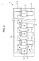
- the thermal head 2 is formed in a flat plate-like shape as shown in a front view of FIG. 2 , and includes a plurality of heating resistor elements 1 at intervals. As shown in a vertical cross sectional view of FIG. 3 , each of the plurality of heating resistor elements 1 includes an insulating substrate 9, a heat accumulating layer 10, a heating resistor 11, and a protective film layer 12 in a laminated state.
- the insulating substrate 9 is bonded to a radiator plate (not shown).
- the insulating substrate 9 and the heat accumulating layer 10 are each formed of alkali-free glass (for example, Corning 1737), and are bonded to each other in a state of adhering to each other through heating to temperature ranging from an annealing point (720°C) to a softening point (975°C) of the material forming the insulating substrate 9 and the heat accumulating layer 10.
- alkali-free glass for example, Corning 1737
- the heat accumulating layer 10 is formed to have a thickness of 2 ⁇ m or more and 100 ⁇ m or less.
- the heating resistor 11 includes a heating resistor layer 13 formed in a predetermined pattern on the heat accumulating layer 10, individual electrodes 14 provided in contact with the heating resistor layer 13 on the heat accumulating layer 10, and a common electrode 15.
- a concave portion 16 is formed in a region opposed to each heating resistor 11.
- an aperture of the concave portion 16 is blocked by a flat surface of the heat accumulating layer 10, with the result that a sealed hollow portion 17 is provided at a position opposed to the heating resistor 11, which is located between the insulating substrate 9 and the heat accumulating layer 10.
- the concave portion 16 may have an appropriate shape, and a size thereof may be larger or smaller compared with the heating resistor 11 as long as the size is close to a size of the heating resistor 11.
- the concave portion 16 When the concave portion 16 is viewed from the heating resistor 11 side in a laminating direction, in a case where the concave portion 16 is made larger than a heating effective area of the heating resistor 11, heat insulating performance between the heating resistor 11 and the insulating substrate 9 can be improved. On the other hand, in a case where the size of the concave portion 16 is made smaller than the heating effective area of the heating resistor 11, a mechanical strength of the heating resistor element 1 with respect to the pressing force in the laminating direction can be improved.
- the concave portion 16 is provided on the insulating substrate 9 side, and is formed in a quadrangle, which substantially has a similar shape as and is slightly larger than the heating resistor 11 when the concave portion 16 is viewed from the heating resistor 11 side in the laminating direction. Further, a depth D of the concave portion 16 is set to 1 ⁇ m or more and 100 ⁇ m or less. In other words, in the heating resistor element 1, a thickness of a gas layer within the hollow portion 17 is sufficiently ensured to be 1 ⁇ m or more, and a heat insulating effect obtained by the gas layer is large. Besides, when the depth D of the concave portion 16 is set to be 100 ⁇ m or less, a thickness size of the heating resistor element 1 can be suppressed to be sufficiently small.
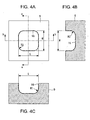
- corners R1, R2, and R3 of the concave portion 16 each are formed in a shape having a curvature radius of 10 ⁇ m or more. Further, an inner surface of the concave portion 16 is formed to have surface roughness Ra of 0.2 ⁇ m or more.
- FIG. 4A is a front view of the concave portion 16, which is viewed from the aperture side
- FIGS. 4B and 4C are vertical cross sectional views taken along a line a-a of FIG. 4A and a line b-b of FIG. 4A , respectively.
- the concave portion 16 having a predetermined depth is formed in a region of a surface of the insulating substrate 9, in which the heating resistor 11 is formed (concave portion forming step).
- the concave portion 16 is formed as follows.
- a photoresist material 18 capable of absorbing an impact of a urethane-based material is applied onto a surface of an alkali-free glass substrate forming the insulating substrate 9 ( FIG. 5A ), and the photoresist material 18 is exposed using a photomask (not shown) having a predetermined pattern, a part other than a region in which the hollow portion 17 is to be formed is solidified, and a part which is not solidified is removed to form a window portion 19 ( FIG. 5B ).
- a part of the insulating substrate 9 corresponding to the window portion 19 is chipped through sandblast processing ( FIG. 5C ).
- the concave portion 16 which has a curvature radius of 10 ⁇ m or more at corners and includes an inner surface of surface roughness Ra of 0.2 ⁇ m or more, can be easily formed.
- the curvature radius of the corner and the surface roughness can be adjusted to a desired value through appropriate adjustments of a shape of the mask, a diameter of a sand particle, a blast pressure, an amount of the sand particles and a spraying angle.
- the surface roughness Ra is less than 0.2 ⁇ m, the diameter of the sand particle needs to be extremely small, and a processing amount (removed amount) per unit time is considerably reduced, which is not suitable for mass production.
- the photoresist material 18 is removed from the surface of the insulating substrate 9 ( FIG. 5D ).
- the concave portion 16 may be formed by high temperature forming using a die in place of the sandblast processing.
- the alkali-free glass substrate serving as the heat accumulating layer 10 is prepared, and is adhered to the bonded surface 9a of the insulating substrate 9 in which the concave portion 16 is formed to block the concave portion 16 ( FIG. 5E ).
- the insulating substrate 9 and the heat accumulating layer 10 are heated to temperature ranging from an annealing point (720°C) to a softening point (975°C) of the alkali-free glass, to thereby bond the insulating substrate 9 and the heat accumulating layer 10 to each other (bonding step).
- a surface opposite to the bonded surface of the heat accumulating layer 10 is removed through etching, polishing, or the like to process the heat accumulating layer 10 to have a desired thickness size (2 ⁇ m to 100 ⁇ m) ( FIG. 5F ).
- the heating resistor layer 13, the individual electrodes 14, the common electrode 15, and the protective film layer 12 are sequentially formed (resistor forming step). Note that the heating resistor layer 13, the individual electrodes 14, the common electrode 15, and the protective film layer 12 may be formed in an appropriate order.
- Those heating resistor layer 13, individual electrodes 14, common electrode 15, and protective film layer 12 can be formed using a manufacturing method for those components of a conventional heating resistor element.
- a thin film forming method such as sputtering, chemical vapor deposition (CVD), or vapor deposition
- a film made of a wiring material such as Al, Al-Si, Au, Ag, Cu, or Pg is formed on the heat accumulating layer 10 by sputtering, vapor deposition, or the like, and then the formed film is molded using the lift-off method or the etching method.
- the wiring material is subjected to screen printing, and then is subjected to baking or the like. Accordingly, the individual electrodes 14 and the common electrode 15 having a desired shape are formed.
- two separate individual electrodes 14 are provided for one heating resistor layer 13, and the common electrode 15 is provided to cover one of the two separate individual electrodes 14 for reducing a wiring resistance value of the common electrode 15.
- the thermal head 2 including the plurality of heating resistor elements 1 according to this embodiment is manufactured.
- the hollow portion 17 is formed in the region between the insulating substrate 9 and the heat accumulating layer 10, which is opposed to the heating resistor 11, and the gas layer formed within the hollow portion 17 functions as the heat insulating layer controlling a flow of heat from the heat accumulating layer 10 to the insulating substrate 9.
- the depth D of the concave portion 16 is 1 ⁇ m or more, and thus a sufficiently thick gas layer is formed, and large heat insulating effects are achieved.
- the thickness of the heat accumulating layer 10 is set to 100 ⁇ m or less, and thus a heat capacity of the heat accumulating layer 10 itself is small, and the heat generated by the heating resistor 11 is prevented from being taken by the heat accumulating layer 10.
- the heat generated by the heating resistor 11 can be effectively used without letting out the heat generated by the heating resistor 11 to the heat accumulating layer 10 side.
- heating efficiency of the heating resistor 11 can be improved to reduce power consumption.
- the heat generated by the heating resistor 11 is difficult to be transmitted to the insulating substrate 9, which has an advantage in that a temperature of the entire thermal head 2 is difficult to increase even after the thermal head 2 is repeatedly used.
- the heat accumulating layer 10 and the insulating substrate 9 are formed of the same glass material, and hence there is no difference in coefficient of thermal expansion, with the result that warp or distortion is not caused by the heat generated by the heating resistor 11.
- the heat accumulating layer 10 and the insulating substrate 9 are formed of the alkali-free glass, and thus alkali ion is not eluted even after the heating resistor element 1 is used for a long period of time.
- the heating resistor 11, the individual electrodes 14, and the common electrode 15 which are located near the heat accumulating layer 10 and the insulating substrate 9, or a driver IC provided in the vicinity thereof can be prevented from being adversely effected by the alkali ion.
- the alkali-free glass is cheaper than Pyrex (registered trademark) glass, and its processibility is excellent, whereby the heating resistor element 1 can be manufactured at low cost.
- a coefficient of thermal conductivity of glass is 0.9 W/mK and a coefficient of thermal conductivity of air is 0.02 W/mK, whereas a coefficient of thermal conductivity of silicon is 168 W/mK.
- the alkali-free glass substrate is employed in place of a conventional silicon substrate, and thus the coefficient of thermal conductivity can be sufficiently reduced, and heat is prevented from being dissipated from the heat accumulating layer 10 through the insulating substrate 9. Accordingly, the heat efficiency can be further increased.
- surface roughness Ra of the inner surface of the concave portion 16, which forms the hollow portion 17 is set to be 0.2 ⁇ m or more, and thus a surface area thereof is increased more compared with the inner surface of a concave portion which is smoothly formed by etching or the like.
- FIGS. 6A and 6B show thermal responsibility of the heating resistor element 1 for each surface roughness of the concave portion 16.
- graphs t1 and t2 show a temperature change of the thermal head 2 when a voltage is applied to the thermal head 2 for a predetermined period of time and then is stopped for a predetermined period of time.
- Graphs t3 and t4 are imaginary curves forming points indicating temperatures of the thermal head 2 before application of a voltage, which are added for easily explaining the thermal head 2 according to the present invention.
- FIG. 6A is a graph showing the thermal responsibility in the case of the smallest surface roughness (Ra: 0.2 ⁇ m) according to this embodiment in contrast with a surface roughness (Ra: 0.02 ⁇ m) according to the prior art
- FIG. 6B is a graph showing the thermal responsibility in the case of the largest surface roughness (Ra: 3 ⁇ m) according to this embodiment in contrast with the surface roughness (Ra: 0.02 ⁇ m) according to the prior art.
- Those graphs show that, in accordance with this embodiment, a rise in temperature due to the use for a long period of time can be suppressed to be smaller compared with the prior art.
- FIG. 7 shows a relationship between the temperature of the heating resistor element 1 and the surface roughness of the inner surface of the hollow portion 17 after the repeated heating of ten pulses is performed (after 0.025 seconds) as shown in FIGS. 6A and 6B .
- the corners R1 to R3 of the concave portion 16 forming the hollow portion 17 are formed in a rounded shape to have the curvature radius of 10 ⁇ m or more, and thus stress concentration caused in the corners R1 to R3 is suppressed, resulting in an improvement of a mechanical strength.
- the heating resistor element 1 having a sufficient mechanical strength can be provided even when the thickness of the heat accumulating layer 10 is set to 2 to 100 ⁇ m. When the heat accumulating layer 10 is made thinner, heating efficiency can be further improved.
- the heat generated by the heating resistor 11 is difficult to be accumulated in the heat accumulating layer 10 or the hollow portion 17 even after the use for a long period of time, with the result that the heat can be efficiently used and the hollow portion 17 can be prevented from becoming a heat source.
- a decrease in printing quality caused by a phenomenon such as tailing can be prevented.
- warp or distortion caused by the difference in coefficient of thermal expansion is not generated in the thermal head 2, and thus the contact between the thermal head 2 and the thermal paper 6 is not changed, which prevents a decrease in printing quality.
- the mechanical strength of the thermal head 2 is large, and thus the thermal head 2 can be maintained in a sound state even when the pressing force repeatedly acts for a long period of time.
- the heating resistor element 1, the thermal head 2, and the thermal printer 3 each having secured long-term reliability and high efficiency can be provided.
- the heat accumulating layer 10 and the insulating substrate 9 made of the same alkali-free glass are bonded to each other through heating to temperature ranging from the annealing point to the softening point of the alkali-free glass, and thus an adhesive layer is not required, and a material for the adhesive layer and the formation step for the adhesive layer are unnecessary. Therefore, the heating resistor element 1 can be easily manufactured in a short period of time at low cost.
- the insulating substrate 9 and the heat accumulating layer 10 are formed of the same alkali-free glass, but not limited thereto, and may be formed of the same soda glass material or the same Pyrex (registered trademark) glass material.
- the insulating substrate 9 and the heat accumulating layer 10 can be also easily bonded to each other through heating to temperature between an annealing point (540°C) and a softening point (730°C) in the case of the soda glass material, and to temperature between an annealing point (565°C) and a softening point (820°C) in the case of the Pyrex (registered trademark) glass material.
- the concave portion 16 provided in the insulating substrate 9 is blocked by the flat heat accumulating layer 10, thereby providing the hollow portion 17 having the inside filled with air.
- the concave portion 16 may be provided in the heat accumulating layer 10 and be blocked by the flat insulating substrate 9 to form the hollow portion 17.
- the concave portions 16 may be provided in both the heat accumulating layer 10 and the insulating substrate 9 to be bonded to each other to form the hollow portion 17.
- the inner surface of the hollow portion 17 provided in the heat accumulating layer 10 is formed smoothly, and the inner surface of the hollow portion 17 provided in the insulating substrate 9 is formed to have the surface roughness Ra of 0.2 ⁇ m or more.
- a thickness of the smallest part of the heat accumulating layer 10 is preferably 2 ⁇ m or more and 100 ⁇ m or less.
- concave portions 16 may be provided on the bonded surfaces of the insulating substrate 9 and the heat accumulating layer 10, respectively, to be combined with each other and thereby form the hollow portion 17.
- the hollow portion 17 may be filled with an inert gas such as N 2 , He, or Ar in place of air.
- an inert gas such as N 2 , He, or Ar in place of air.
- the hollow portion 17 may be completely sealed and the pressure within the hollow portion 17 may be reduced to an atmospheric pressure or less. As a result, heat insulating effect obtained by the hollow portion 17 can be improved.
- the hollow portion 17 is individually provided to be opposed to the each heating resistor 11.
- the concave portion 16 and the hollow portion 17 described above there may be provided a common concave portion 16' and a common hollow portion 17' which are provided to be opposed to the plurality of heating resistors 11.
Landscapes
- Engineering & Computer Science (AREA)
- Manufacturing & Machinery (AREA)
- Chemical & Material Sciences (AREA)
- Ceramic Engineering (AREA)
- Inorganic Chemistry (AREA)
- Physics & Mathematics (AREA)
- General Physics & Mathematics (AREA)
- Electronic Switches (AREA)
Applications Claiming Priority (2)
| Application Number | Priority Date | Filing Date | Title |
|---|---|---|---|
| JP2007275593 | 2007-10-23 | ||
| JP2008218635A JP2009119850A (ja) | 2007-10-23 | 2008-08-27 | 発熱抵抗素子とその製造方法、サーマルヘッドおよびプリンタ |
Publications (3)
| Publication Number | Publication Date |
|---|---|
| EP2053901A2 true EP2053901A2 (de) | 2009-04-29 |
| EP2053901A3 EP2053901A3 (de) | 2011-01-12 |
| EP2053901B1 EP2053901B1 (de) | 2012-09-12 |
Family
ID=40220033
Family Applications (1)
| Application Number | Title | Priority Date | Filing Date |
|---|---|---|---|
| EP08253445A Ceased EP2053901B1 (de) | 2007-10-23 | 2008-10-23 | Heizwiderstandselement, Herstellungsverfahren dafür, Thermokopf und Drucker |
Country Status (2)
| Country | Link |
|---|---|
| US (1) | US7768541B2 (de) |
| EP (1) | EP2053901B1 (de) |
Cited By (1)
| Publication number | Priority date | Publication date | Assignee | Title |
|---|---|---|---|---|
| CN102152647A (zh) * | 2009-12-17 | 2011-08-17 | 精工电子有限公司 | 热头及打印机 |
Families Citing this family (18)
| Publication number | Priority date | Publication date | Assignee | Title |
|---|---|---|---|---|
| US8144175B2 (en) | 2007-10-23 | 2012-03-27 | Seiko Instruments Inc. | Heating resistor element, manufacturing method for the same, thermal head, and printer |
| JP5421680B2 (ja) * | 2009-07-21 | 2014-02-19 | セイコーインスツル株式会社 | サーマルヘッドの製造方法、サーマルヘッドおよびプリンタ |
| JP5424386B2 (ja) * | 2009-07-29 | 2014-02-26 | セイコーインスツル株式会社 | サーマルヘッドおよびプリンタ |
| JP5424387B2 (ja) * | 2009-08-06 | 2014-02-26 | セイコーインスツル株式会社 | サーマルヘッドおよびサーマルヘッドの製造方法 |
| JP5541660B2 (ja) * | 2009-08-06 | 2014-07-09 | セイコーインスツル株式会社 | サーマルヘッドの製造方法 |
| JP5366088B2 (ja) * | 2009-09-16 | 2013-12-11 | セイコーインスツル株式会社 | サーマルヘッドおよびプリンタ |
| JP5668910B2 (ja) * | 2010-03-08 | 2015-02-12 | セイコーインスツル株式会社 | サーマルヘッド、プリンタおよびサーマルヘッドの製造方法 |
| JP5672479B2 (ja) * | 2010-08-25 | 2015-02-18 | セイコーインスツル株式会社 | サーマルヘッド、プリンタおよびサーマルヘッドの製造方法 |
| JP5697017B2 (ja) * | 2010-09-22 | 2015-04-08 | セイコーインスツル株式会社 | ヘッドユニット、プリンタおよびヘッドユニットの製造方法 |
| JP5787248B2 (ja) * | 2010-09-24 | 2015-09-30 | セイコーインスツル株式会社 | サーマルヘッドの製造方法 |
| JP5787247B2 (ja) * | 2010-09-24 | 2015-09-30 | セイコーインスツル株式会社 | サーマルヘッドの製造方法 |
| JP5765845B2 (ja) * | 2011-02-23 | 2015-08-19 | セイコーインスツル株式会社 | サーマルヘッドおよびその製造方法、並びにプリンタ |
| JP5765844B2 (ja) * | 2011-02-23 | 2015-08-19 | セイコーインスツル株式会社 | サーマルヘッドおよびその製造方法、並びにプリンタ |
| JP2013139095A (ja) * | 2011-12-28 | 2013-07-18 | Seiko Instruments Inc | サーマルヘッド、プリンタおよびサーマルヘッドの製造方法 |
| JP6021142B2 (ja) * | 2012-06-19 | 2016-11-09 | セイコーインスツル株式会社 | サーマルヘッド、プリンタおよびサーマルヘッドの製造方法 |
| JP6767415B2 (ja) * | 2018-03-20 | 2020-10-14 | 株式会社東芝 | 定着装置及び画像形成装置 |
| CN110466243B (zh) * | 2018-05-11 | 2022-08-23 | 重庆莱宝科技有限公司 | 一种自动丝印方法 |
| JP7512106B2 (ja) * | 2020-07-15 | 2024-07-08 | キヤノン株式会社 | 定着装置及び画像形成装置 |
Citations (1)
| Publication number | Priority date | Publication date | Assignee | Title |
|---|---|---|---|---|
| JP2007083532A (ja) | 2005-09-22 | 2007-04-05 | Seiko Instruments Inc | 発熱抵抗素子、サーマルヘッド、プリンタ、及び発熱抵抗素子の製造方法 |
Family Cites Families (4)
| Publication number | Priority date | Publication date | Assignee | Title |
|---|---|---|---|---|
| US5357271A (en) * | 1993-01-19 | 1994-10-18 | Intermec Corporation | Thermal printhead with enhanced laterla heat conduction |
| CN1086639C (zh) * | 1994-05-31 | 2002-06-26 | 罗姆股份有限公司 | 感热式打印头、打印头中所用基板及该基板的制造方法 |
| CN1086640C (zh) * | 1994-06-21 | 2002-06-26 | 罗姆股份有限公司 | 热打印头和用于打印头的基片以及该基片的制造方法 |
| JP5039940B2 (ja) * | 2005-10-25 | 2012-10-03 | セイコーインスツル株式会社 | 発熱抵抗素子、サーマルヘッド、プリンタ、及び発熱抵抗素子の製造方法 |
-
2008
- 2008-10-20 US US12/254,504 patent/US7768541B2/en not_active Expired - Fee Related
- 2008-10-23 EP EP08253445A patent/EP2053901B1/de not_active Ceased
Patent Citations (1)
| Publication number | Priority date | Publication date | Assignee | Title |
|---|---|---|---|---|
| JP2007083532A (ja) | 2005-09-22 | 2007-04-05 | Seiko Instruments Inc | 発熱抵抗素子、サーマルヘッド、プリンタ、及び発熱抵抗素子の製造方法 |
Cited By (2)
| Publication number | Priority date | Publication date | Assignee | Title |
|---|---|---|---|---|
| CN102152647A (zh) * | 2009-12-17 | 2011-08-17 | 精工电子有限公司 | 热头及打印机 |
| CN102152647B (zh) * | 2009-12-17 | 2014-12-24 | 精工电子有限公司 | 热头及打印机 |
Also Published As
| Publication number | Publication date |
|---|---|
| EP2053901A3 (de) | 2011-01-12 |
| US20090102911A1 (en) | 2009-04-23 |
| US7768541B2 (en) | 2010-08-03 |
| EP2053901B1 (de) | 2012-09-12 |
Similar Documents
| Publication | Publication Date | Title |
|---|---|---|
| EP2053901B1 (de) | Heizwiderstandselement, Herstellungsverfahren dafür, Thermokopf und Drucker | |
| US8850691B2 (en) | Manufacturing method for a heating resistor element | |
| CN101417545B (zh) | 加热电阻元件及其制造方法、热敏头和打印机 | |
| EP2056648B1 (de) | Heizwiderstandselement, Herstellungsverfahren dafür, Thermokopf und Drucker | |
| US7522178B2 (en) | Heating resistance element, thermal head, printer, and method of manufacturing heating resistance element | |
| CN101417544A (zh) | 加热电阻元件及其制造方法、热敏头和打印机 | |
| US8111273B2 (en) | Thermal head, printer, and manufacturing method for thermal head | |
| EP2179850A2 (de) | Thermokopfherstellungsverfahren, Thermokopf und Drucker | |
| CN101417546B (zh) | 加热电阻元件的制造方法 | |
| EP2298562B1 (de) | Thermokopf und Drucker | |
| US8189019B2 (en) | Thermal head, thermal printer, and manufacturing method for thermal head | |
| US8998385B2 (en) | Thermal head, printer, and method of manufacturing thermal head | |
| US9302495B2 (en) | Thermal head, printer, and method of manufacturing thermal head | |
| JP5273786B2 (ja) | サーマルヘッド、プリンタおよびサーマルヘッドの製造方法 | |
| US5473357A (en) | Thermal head and manufacturing method | |
| JP2018034407A (ja) | サーマルプリントヘッドおよびサーマルプリンタ | |
| US8189020B2 (en) | Thermal head, thermal printer, and manufacturing method for thermal head | |
| JP2002307733A (ja) | サーマルヘッドおよびその製造方法 | |
| JPH11138879A (ja) | サーマルヘッド用基板 | |
| US8440943B2 (en) | Heating resistor element component and method of manufacturing heating resistor element component | |
| JP2007137687A (ja) | 成形型 | |
| JPH05147248A (ja) | サ−マルヘツド及びその製造方法 | |
| JPH10100458A (ja) | サーマルヘッド及びその製造方法 | |
| JP2004291512A (ja) | サーマルヘッド及びその製造方法、並びにサーマルプリンタ |
Legal Events
| Date | Code | Title | Description |
|---|---|---|---|
| PUAI | Public reference made under article 153(3) epc to a published international application that has entered the european phase |
Free format text: ORIGINAL CODE: 0009012 |
|
| AK | Designated contracting states |
Kind code of ref document: A2 Designated state(s): AT BE BG CH CY CZ DE DK EE ES FI FR GB GR HR HU IE IS IT LI LT LU LV MC MT NL NO PL PT RO SE SI SK TR |
|
| AX | Request for extension of the european patent |
Extension state: AL BA MK RS |
|
| PUAL | Search report despatched |
Free format text: ORIGINAL CODE: 0009013 |
|
| AK | Designated contracting states |
Kind code of ref document: A3 Designated state(s): AT BE BG CH CY CZ DE DK EE ES FI FR GB GR HR HU IE IS IT LI LT LU LV MC MT NL NO PL PT RO SE SI SK TR |
|
| AX | Request for extension of the european patent |
Extension state: AL BA MK RS |
|
| 17P | Request for examination filed |
Effective date: 20110712 |
|
| AKX | Designation fees paid |
Designated state(s): DE FR GB IT |
|
| GRAP | Despatch of communication of intention to grant a patent |
Free format text: ORIGINAL CODE: EPIDOSNIGR1 |
|
| GRAS | Grant fee paid |
Free format text: ORIGINAL CODE: EPIDOSNIGR3 |
|
| GRAA | (expected) grant |
Free format text: ORIGINAL CODE: 0009210 |
|
| AK | Designated contracting states |
Kind code of ref document: B1 Designated state(s): DE FR GB IT |
|
| REG | Reference to a national code |
Ref country code: GB Ref legal event code: FG4D |
|
| REG | Reference to a national code |
Ref country code: DE Ref legal event code: R096 Ref document number: 602008018698 Country of ref document: DE Effective date: 20121108 |
|
| PLBE | No opposition filed within time limit |
Free format text: ORIGINAL CODE: 0009261 |
|
| STAA | Information on the status of an ep patent application or granted ep patent |
Free format text: STATUS: NO OPPOSITION FILED WITHIN TIME LIMIT |
|
| 26N | No opposition filed |
Effective date: 20130613 |
|
| REG | Reference to a national code |
Ref country code: DE Ref legal event code: R097 Ref document number: 602008018698 Country of ref document: DE Effective date: 20130613 |
|
| REG | Reference to a national code |
Ref country code: FR Ref legal event code: PLFP Year of fee payment: 9 |
|
| REG | Reference to a national code |
Ref country code: FR Ref legal event code: PLFP Year of fee payment: 10 |
|
| PGFP | Annual fee paid to national office [announced via postgrant information from national office to epo] |
Ref country code: FR Payment date: 20170918 Year of fee payment: 10 |
|
| PGFP | Annual fee paid to national office [announced via postgrant information from national office to epo] |
Ref country code: IT Payment date: 20171024 Year of fee payment: 10 Ref country code: GB Payment date: 20171018 Year of fee payment: 10 |
|
| GBPC | Gb: european patent ceased through non-payment of renewal fee |
Effective date: 20181023 |
|
| PG25 | Lapsed in a contracting state [announced via postgrant information from national office to epo] |
Ref country code: FR Free format text: LAPSE BECAUSE OF NON-PAYMENT OF DUE FEES Effective date: 20181031 |
|
| PG25 | Lapsed in a contracting state [announced via postgrant information from national office to epo] |
Ref country code: IT Free format text: LAPSE BECAUSE OF NON-PAYMENT OF DUE FEES Effective date: 20181023 Ref country code: GB Free format text: LAPSE BECAUSE OF NON-PAYMENT OF DUE FEES Effective date: 20181023 |
|
| PGFP | Annual fee paid to national office [announced via postgrant information from national office to epo] |
Ref country code: DE Payment date: 20191008 Year of fee payment: 12 |
|
| REG | Reference to a national code |
Ref country code: DE Ref legal event code: R119 Ref document number: 602008018698 Country of ref document: DE |
|
| PG25 | Lapsed in a contracting state [announced via postgrant information from national office to epo] |
Ref country code: DE Free format text: LAPSE BECAUSE OF NON-PAYMENT OF DUE FEES Effective date: 20210501 |