EP2050150B1 - Procédé de fabrication d'au moins un corps multicouche et corps multicouche - Google Patents
Procédé de fabrication d'au moins un corps multicouche et corps multicouche Download PDFInfo
- Publication number
- EP2050150B1 EP2050150B1 EP07801506.2A EP07801506A EP2050150B1 EP 2050150 B1 EP2050150 B1 EP 2050150B1 EP 07801506 A EP07801506 A EP 07801506A EP 2050150 B1 EP2050150 B1 EP 2050150B1
- Authority
- EP
- European Patent Office
- Prior art keywords
- layer
- region
- carrier substrate
- relief structure
- functional layer
- Prior art date
- Legal status (The legal status is an assumption and is not a legal conclusion. Google has not performed a legal analysis and makes no representation as to the accuracy of the status listed.)
- Not-in-force
Links
- 238000004519 manufacturing process Methods 0.000 title claims description 12
- 239000010410 layer Substances 0.000 claims description 166
- 239000002346 layers by function Substances 0.000 claims description 146
- 239000000758 substrate Substances 0.000 claims description 113
- 230000005855 radiation Effects 0.000 claims description 61
- 238000000034 method Methods 0.000 claims description 29
- 239000000463 material Substances 0.000 claims description 26
- 230000005669 field effect Effects 0.000 claims description 7
- 239000003990 capacitor Substances 0.000 claims description 4
- 239000011521 glass Substances 0.000 claims description 2
- 229910001092 metal group alloy Inorganic materials 0.000 claims description 2
- 239000002966 varnish Substances 0.000 claims description 2
- 239000003973 paint Substances 0.000 claims 10
- 230000003362 replicative effect Effects 0.000 claims 1
- 229920002120 photoresistant polymer Polymers 0.000 description 33
- 230000003287 optical effect Effects 0.000 description 20
- 230000005540 biological transmission Effects 0.000 description 19
- 238000005530 etching Methods 0.000 description 16
- 230000010287 polarization Effects 0.000 description 11
- 230000015572 biosynthetic process Effects 0.000 description 7
- 230000000694 effects Effects 0.000 description 7
- 230000035699 permeability Effects 0.000 description 6
- 229910052709 silver Inorganic materials 0.000 description 6
- 239000010931 gold Substances 0.000 description 5
- 238000012545 processing Methods 0.000 description 5
- 230000008859 change Effects 0.000 description 4
- 239000010408 film Substances 0.000 description 4
- 229910052737 gold Inorganic materials 0.000 description 4
- 229910052751 metal Inorganic materials 0.000 description 4
- 239000002184 metal Substances 0.000 description 4
- 239000002105 nanoparticle Substances 0.000 description 4
- 239000002985 plastic film Substances 0.000 description 4
- 229920000642 polymer Polymers 0.000 description 4
- 230000008569 process Effects 0.000 description 4
- 239000004065 semiconductor Substances 0.000 description 4
- 239000004332 silver Substances 0.000 description 4
- 238000004544 sputter deposition Methods 0.000 description 4
- 238000007740 vapor deposition Methods 0.000 description 4
- 239000010949 copper Substances 0.000 description 3
- 230000001419 dependent effect Effects 0.000 description 3
- 238000011161 development Methods 0.000 description 3
- 239000007788 liquid Substances 0.000 description 3
- 238000000059 patterning Methods 0.000 description 3
- 239000000049 pigment Substances 0.000 description 3
- 229920006255 plastic film Polymers 0.000 description 3
- RYGMFSIKBFXOCR-UHFFFAOYSA-N Copper Chemical compound [Cu] RYGMFSIKBFXOCR-UHFFFAOYSA-N 0.000 description 2
- 208000027418 Wounds and injury Diseases 0.000 description 2
- 239000012790 adhesive layer Substances 0.000 description 2
- 229910052782 aluminium Inorganic materials 0.000 description 2
- 230000008901 benefit Effects 0.000 description 2
- 238000004364 calculation method Methods 0.000 description 2
- 239000011248 coating agent Substances 0.000 description 2
- 238000000576 coating method Methods 0.000 description 2
- 239000004020 conductor Substances 0.000 description 2
- 229910052802 copper Inorganic materials 0.000 description 2
- 230000007423 decrease Effects 0.000 description 2
- PCHJSUWPFVWCPO-UHFFFAOYSA-N gold Chemical compound [Au] PCHJSUWPFVWCPO-UHFFFAOYSA-N 0.000 description 2
- 238000005286 illumination Methods 0.000 description 2
- 239000004973 liquid crystal related substance Substances 0.000 description 2
- 239000011368 organic material Substances 0.000 description 2
- 230000000737 periodic effect Effects 0.000 description 2
- 230000000704 physical effect Effects 0.000 description 2
- 238000002360 preparation method Methods 0.000 description 2
- 150000003384 small molecules Chemical class 0.000 description 2
- 238000005507 spraying Methods 0.000 description 2
- 239000000725 suspension Substances 0.000 description 2
- 238000010345 tape casting Methods 0.000 description 2
- 239000012815 thermoplastic material Substances 0.000 description 2
- 238000012546 transfer Methods 0.000 description 2
- 238000002834 transmittance Methods 0.000 description 2
- 206010004966 Bite Diseases 0.000 description 1
- XMWRBQBLMFGWIX-UHFFFAOYSA-N C60 fullerene Chemical class C12=C3C(C4=C56)=C7C8=C5C5=C9C%10=C6C6=C4C1=C1C4=C6C6=C%10C%10=C9C9=C%11C5=C8C5=C8C7=C3C3=C7C2=C1C1=C2C4=C6C4=C%10C6=C9C9=C%11C5=C5C8=C3C3=C7C1=C1C2=C4C6=C2C9=C5C3=C12 XMWRBQBLMFGWIX-UHFFFAOYSA-N 0.000 description 1
- OKTJSMMVPCPJKN-UHFFFAOYSA-N Carbon Chemical compound [C] OKTJSMMVPCPJKN-UHFFFAOYSA-N 0.000 description 1
- 239000000654 additive Substances 0.000 description 1
- 230000000996 additive effect Effects 0.000 description 1
- XAGFODPZIPBFFR-UHFFFAOYSA-N aluminium Chemical compound [Al] XAGFODPZIPBFFR-UHFFFAOYSA-N 0.000 description 1
- 229910052799 carbon Inorganic materials 0.000 description 1
- 239000000969 carrier Substances 0.000 description 1
- 238000006243 chemical reaction Methods 0.000 description 1
- 229910052804 chromium Inorganic materials 0.000 description 1
- 239000011651 chromium Substances 0.000 description 1
- 238000007796 conventional method Methods 0.000 description 1
- 229910021419 crystalline silicon Inorganic materials 0.000 description 1
- 238000013461 design Methods 0.000 description 1
- 239000003989 dielectric material Substances 0.000 description 1
- 238000009826 distribution Methods 0.000 description 1
- 230000009977 dual effect Effects 0.000 description 1
- 239000000839 emulsion Substances 0.000 description 1
- 238000002474 experimental method Methods 0.000 description 1
- 229910052732 germanium Inorganic materials 0.000 description 1
- GNPVGFCGXDBREM-UHFFFAOYSA-N germanium atom Chemical compound [Ge] GNPVGFCGXDBREM-UHFFFAOYSA-N 0.000 description 1
- 238000001746 injection moulding Methods 0.000 description 1
- 239000004922 lacquer Substances 0.000 description 1
- 230000031700 light absorption Effects 0.000 description 1
- 238000010327 methods by industry Methods 0.000 description 1
- 238000002156 mixing Methods 0.000 description 1
- 239000000203 mixture Substances 0.000 description 1
- 238000000465 moulding Methods 0.000 description 1
- 239000002077 nanosphere Substances 0.000 description 1
- 230000001151 other effect Effects 0.000 description 1
- 239000005022 packaging material Substances 0.000 description 1
- SLIUAWYAILUBJU-UHFFFAOYSA-N pentacene Chemical compound C1=CC=CC2=CC3=CC4=CC5=CC=CC=C5C=C4C=C3C=C21 SLIUAWYAILUBJU-UHFFFAOYSA-N 0.000 description 1
- 238000000206 photolithography Methods 0.000 description 1
- 229920003023 plastic Polymers 0.000 description 1
- 229920001296 polysiloxane Polymers 0.000 description 1
- 238000004080 punching Methods 0.000 description 1
- 230000009467 reduction Effects 0.000 description 1
- 230000010076 replication Effects 0.000 description 1
- 238000000926 separation method Methods 0.000 description 1
- 125000006850 spacer group Chemical group 0.000 description 1
- 230000003595 spectral effect Effects 0.000 description 1
- 239000010409 thin film Substances 0.000 description 1
- 229910052719 titanium Inorganic materials 0.000 description 1
- 239000010936 titanium Substances 0.000 description 1
- 238000012549 training Methods 0.000 description 1
- 230000000007 visual effect Effects 0.000 description 1
Images


Classifications
-
- H—ELECTRICITY
- H10—SEMICONDUCTOR DEVICES; ELECTRIC SOLID-STATE DEVICES NOT OTHERWISE PROVIDED FOR
- H10K—ORGANIC ELECTRIC SOLID-STATE DEVICES
- H10K71/00—Manufacture or treatment specially adapted for the organic devices covered by this subclass
- H10K71/20—Changing the shape of the active layer in the devices, e.g. patterning
- H10K71/231—Changing the shape of the active layer in the devices, e.g. patterning by etching of existing layers
- H10K71/233—Changing the shape of the active layer in the devices, e.g. patterning by etching of existing layers by photolithographic etching
-
- H—ELECTRICITY
- H10—SEMICONDUCTOR DEVICES; ELECTRIC SOLID-STATE DEVICES NOT OTHERWISE PROVIDED FOR
- H10K—ORGANIC ELECTRIC SOLID-STATE DEVICES
- H10K10/00—Organic devices specially adapted for rectifying, amplifying, oscillating or switching; Organic capacitors or resistors having potential barriers
- H10K10/40—Organic transistors
- H10K10/46—Field-effect transistors, e.g. organic thin-film transistors [OTFT]
- H10K10/462—Insulated gate field-effect transistors [IGFETs]
- H10K10/464—Lateral top-gate IGFETs comprising only a single gate
-
- Y—GENERAL TAGGING OF NEW TECHNOLOGICAL DEVELOPMENTS; GENERAL TAGGING OF CROSS-SECTIONAL TECHNOLOGIES SPANNING OVER SEVERAL SECTIONS OF THE IPC; TECHNICAL SUBJECTS COVERED BY FORMER USPC CROSS-REFERENCE ART COLLECTIONS [XRACs] AND DIGESTS
- Y02—TECHNOLOGIES OR APPLICATIONS FOR MITIGATION OR ADAPTATION AGAINST CLIMATE CHANGE
- Y02E—REDUCTION OF GREENHOUSE GAS [GHG] EMISSIONS, RELATED TO ENERGY GENERATION, TRANSMISSION OR DISTRIBUTION
- Y02E10/00—Energy generation through renewable energy sources
- Y02E10/50—Photovoltaic [PV] energy
- Y02E10/549—Organic PV cells
-
- Y—GENERAL TAGGING OF NEW TECHNOLOGICAL DEVELOPMENTS; GENERAL TAGGING OF CROSS-SECTIONAL TECHNOLOGIES SPANNING OVER SEVERAL SECTIONS OF THE IPC; TECHNICAL SUBJECTS COVERED BY FORMER USPC CROSS-REFERENCE ART COLLECTIONS [XRACs] AND DIGESTS
- Y10—TECHNICAL SUBJECTS COVERED BY FORMER USPC
- Y10T—TECHNICAL SUBJECTS COVERED BY FORMER US CLASSIFICATION
- Y10T428/00—Stock material or miscellaneous articles
- Y10T428/24—Structurally defined web or sheet [e.g., overall dimension, etc.]
- Y10T428/24479—Structurally defined web or sheet [e.g., overall dimension, etc.] including variation in thickness
- Y10T428/24612—Composite web or sheet
-
- Y—GENERAL TAGGING OF NEW TECHNOLOGICAL DEVELOPMENTS; GENERAL TAGGING OF CROSS-SECTIONAL TECHNOLOGIES SPANNING OVER SEVERAL SECTIONS OF THE IPC; TECHNICAL SUBJECTS COVERED BY FORMER USPC CROSS-REFERENCE ART COLLECTIONS [XRACs] AND DIGESTS
- Y10—TECHNICAL SUBJECTS COVERED BY FORMER USPC
- Y10T—TECHNICAL SUBJECTS COVERED BY FORMER US CLASSIFICATION
- Y10T428/00—Stock material or miscellaneous articles
- Y10T428/24—Structurally defined web or sheet [e.g., overall dimension, etc.]
- Y10T428/24802—Discontinuous or differential coating, impregnation or bond [e.g., artwork, printing, retouched photograph, etc.]
Definitions
- the invention relates to a method for producing a multilayer body, in particular a multilayer body having at least one electronic component, wherein the multilayer body comprises at least two functional layers, in particular electrical functional layers, on an upper side of a carrier substrate, which are structured in register with one another.
- the invention further relates to a multi-layer body obtainable thereafter.
- OFET organic field effect transistors
- the field-effect transistors are formed from a plurality of functional layers or functional layers, which are applied to the carrier substrate, in particular by printing or knife coating.
- the carrier substrate is formed inter alia as a plastic film with a thickness in the range of 6 to 200 microns.
- Thick support substrates have heretofore been preferred because processing of thinner, less costly support substrates having a thickness in the range of 6 to about 50 microns has been found to be prone to distortion during processing, with the distortion varying with each processing step. If an electrical functional layer is applied and patterned on the thin carrier substrate, a noticeable distortion or perpendicular to the carrier substrate already results in a deviation of the shape of the functional layer from its ideal shape. The delay has a particularly disturbing effect if, subsequently or after application of one or more full-surface functional layers, combined with a further change in the dimensions of the already formed structured functional layer, a further structured functional layer must be arranged in the register relative to the already formed structured functional layer.
- the object is achieved for the method for producing a multilayer body, which comprises at least two, in particular electrically functional layers on an upper side of a carrier substrate, which are structured in register to each other, that a bottom of the carrier substrate is prepared such that in a first region, a permeability for a first exposure radiation and in at least one second region, a transmission for at least one different second exposure radiation in the register to the first region results in that the bottom is successively exposed to the first and the at least one second exposure radiation, and that the first exposure radiation for structuring a first functional layer and the at least one second exposure radiation is used for structuring at least one second functional layer on the upper side of the carrier substrate.
- the method according to the invention makes possible an unproblematic arrangement of the at least one second functional layer in the perfect or nearly perfect register to the first functional layer, since the distortion occurring equally affects the first region and the at least one second region.
- the shape of the first region is changed perpendicular to the plane of the carrier substrate in accordance with the shape of the at least one second region by the distortion, so that the position of the first region with respect to the position of the at least one second region can not shift.
- the position of the first region and of the at least one second region is thus already established on the carrier substrate at the beginning of the production process, so that an inaccuracy in the orientation of the first functional layer relative to the at least one second functional layer can no longer occur despite a distortion of the carrier substrate.
- the at least one second functional layer is formed in a position that is different from its ideal shape and in a shape adapted to the currently present form of the first functional layer, in a positionally accurate manner relative to the first functional layer. Due to the precise positioning of the functional layers relative to one another, it is now possible to form high-quality optical and / or electrical components with improved optical or electrical properties while at the same time requiring less space on the carrier substrate.
- the method according to the invention is furthermore particularly suitable for the production of optical components which comprise two structured functional layers separated from one another by a spacer layer.
- the two structured functional layers may be metallic or colored layers.
- the first functional layer is preferably an opaque mask layer which, when viewed, effects an angle-dependent geometrical shadowing of the second structured functional layer and thus generates, for example, a color flip or a change in the displayed image information depending on the viewing angle.
- the two or more independently structurable functional layers are directly adjacent to each other and thus form, for example, a color image by additive or subtractive color mixing.
- the functional layers may also be IR or UV-luminescent layers structurable independently of one another or layers which are provided with optically variable pigments (thin-film layer pigments, liquid crystal pigments).
- the optical functional layers may be superimposed on a diffractive surface relief and thus represent, for example, metallic or dielectric reflection layers which enable the generation of a partially present optically variable effect (for example a hologram).
- the carrier substrate on the underside directly with relief structures or to provide a layer applied to the underside, in particular of a thermoplastic material or a UV coating, with relief structures.
- an injection molding tool can be used or the relief structures can be formed by molding a stamp in UV varnish or by means of an optionally heated stamp in thermoplastic material.
- the use of a classical photolithography method to form the relief structures on the bottom Of the carrier substrate, in which a photoresist is applied, exposed, developed and used as an etching mask for the bottom, is readily possible.
- a multilayer body in particular comprising an organic electronic component, which has a carrier substrate made of a flexible film material, in particular a plastic film material, characterized in that an underside of the carrier substrate is prepared such that in a first region, a permeability to a first At least two structured functional layers in register with each other and further in the register to the first and the at least one second on a top side of the carrier substrate at least one second exposure radiation is formed in the register to the first region Area are arranged.
- the carrier substrate in this case has a thickness in the range of 3 .mu.m to 250 .mu.m, preferably 6 .mu.m to 50 .mu.m.
- the first and second exposure radiation may differ, for example, by their wavelength, polarization, spectral composition, the angle of incidence of illumination, etc.
- the component Due to the precise positioning of the functional layers relative to one another, the component has particularly good and reproducible optical and / or electrical properties while at the same time requiring little space.
- the underside of the carrier substrate is prepared by a first relief structure in the first region and in the second region and in register with the first relief structure at least one second relief structure different from the first relief structure is formed so that an exposure mask layer is applied to the underside, wherein the exposure mask layer is applied with a constant areal density relative to a plane spanned by the carrier layer, that in the register to the first relief structure that on top
- the first functional layer applied to the carrier substrate is structured, and the at least one second electrical functional layer applied to the upper side of the carrier substrate is patterned in register with the at least one second relief structure.
- no exposure mask layer is needed.
- the first variant of the method is based on the finding that physical properties of the exposure mask layer applied to the carrier substrate, for example effective thickness or optical density, are influenced by the relief structures in the first and at least one second area, so that the transmission properties of the exposure mask layer in the first and second area differ.
- the exposure mask layer is used in an exposure method as a mask for the partial removal of the first electrical functional layer and also for the partial removal of the at least one second electrical functional layer, in each case by passing a photosensitive layer on the upper side of the carrier substrate through the exposure mask layer, ie also through the carrier substrate is exposed and partially removed, so that a structuring of the first and the second functional layer is carried out immediately or can be done afterwards.
- the advantage is achieved that they are aligned in register with each other without additional adjustment effort. Only the Tolerances of the relief structures Influence on the tolerances of the position of the two functional layers. The arrangement of areas of the exposure mask layer with the same physical properties takes place exactly in register with the first and at least one second area.
- the carrier substrate should be as thin as possible, since the distance between the structured layer and the e.g. photoactive layer on the opposite side, especially with thick carriers, may have an impact on the quality / resolution / register of the functional layer.
- the exposure mask layer is a layer that performs a dual function because it provides the function of a high-precision exposure mask for the manufacturing process of differently structured functional layers.
- the exposure mask layer is preferably applied to the carrier substrate by means of sputtering, vapor deposition or spraying.
- a directed material order when sputtering is due to the process, a directed material order, so that when sputtering material of the exposure mask layer in constant area density based on the plane spanned by the carrier substrate plane, the material is locally deposited differently thick on the provided with the relief structures carrier substrate.
- an at least partially directed material application is preferably also produced by process engineering. The material application can be done not only vertically, but also at an angle in the range of 30 to 150 ° to the plane spanned by the carrier substrate level. This is particularly advantageous when using periodic symmetric or asymmetrical relief structures, which are selectively coated in a targeted manner should be.
- the exposure mask layer is preferably formed by a metal layer or by a layer of a metal alloy.
- a metal layer can be applied by known methods, such as sputtering, and they have a sufficient optical density even at low layer thicknesses.
- the exposure mask layer can also be a nonmetallic layer, which can be colored, for example, can contain liquid crystals or can be doped, for example with nanoparticles or with nano spheres, in order to increase their optical density.
- the exposure mask layer is applied to the carrier substrate in a thickness at which the exposure mask layer is substantially opaque, preferably has an optical density of greater than 1.5.
- the exposure mask layer is applied to the carrier substrate over its entire surface in a thickness at which the exposure mask layer has an optical density between 2 and 7.
- the first and the second relief structure may be in the first region as a first relief structure, a diffractive relief structure with a high depth-to-width ratio of the individual structural elements, in particular with a depth-to-width ratio> 0.3, molded and the second relief structure be formed as a relief structure with lower depth-to-width ratio.
- the photosensitive layer is exposed through the exposure mask layer by means of UV radiation.
- UV radiation Experiments have shown that the differences in the transmission properties of the exposure mask layer in the region of the UV radiation which can be achieved by the different design of the relief structure in the first and second regions are particularly pronounced. When using UV radiation for the exposure, particularly good results can be achieved.
- Relief structures with small differences in the depth-to-width ratio also usually show relatively small differences in transmission with thin vapor deposition. Even small relative differences However, they can be enhanced by increasing the layer thickness of the exposure mask layer and thus the average optical density. Thus, even with quite small differences in the transmission of the exposure mask layer in the first and in the second range, good results can be achieved.
- the exposure mask layer may be a very thin layer, on the order of a few nm.
- the exposure mask layer applied with uniform areal density relative to the plane defined by the carrier substrate is made substantially thinner in areas having a high depth-to-width ratio than in areas having a lower depth-to-width ratio.
- the dimensionless depth-to-width ratio h / d is a characteristic feature for the enlargement of the surface when using preferably periodic structures, for example with a sinusoidal course.
- Depth is the distance between the highest and the lowest consecutive point of such a structure, ie the distance between "mountain” and “valley”.
- Width is the distance between two adjacent highest points, ie between two "mountains”.
- the effect of forming higher transmission or transparency as the depth-to-width ratio increases is also observed in structures having vertical edges, such as rectangular gratings. But they can also be structures to which this model is not applicable.
- they may be discretely distributed line-shaped areas which are formed only as a "valley", wherein the distance between two “valleys” is many times higher than the depth of the "valleys".
- the thus calculated depth-to-width ratio would be close to zero and do not reflect the characteristic physical behavior. Therefore, with discretely arranged structures formed essentially only of a "valley”, the depth of the "valley” should be related to the width of the "valley".
- the degree of optical density reduction may vary depending on the background, lighting, etc. An important role is played by the absorption of light in the exposure mask layer.
- silver and gold have a high maximum reflectance R Max and require a relatively small depth to width ratio to reduce the optical density of the metallic exposure mask layer in the above Example of training for transparency.
- aluminum also has a high maximum reflectance R Max , it requires a higher depth-to-width ratio. Preferably, therefore, it may be provided to form the exposure mask layer of silver or gold.
- Table 2 now shows the calculation results obtained from strict diffraction calculations for relief structures formed as linear, sinusoidal gratings with a grid spacing of 350 nm with different depth-to-width ratios.
- the degree of transparency or the reflectance of the exposure masks is wavelength-dependent. This effect is especially good for TE polarized light.
- the degree of transparency or transmission decreases when the angle of incidence of the light differs from the normal angle of incidence, i. the degree of transparency decreases when the light is not incident vertically.
- the exposure mask layer can be made transparent or transparent only in a limited incidence cone of the light. It can thus be provided that the exposure mask layer is formed opaque or impermeable in oblique illumination, whereby this effect can be used for the selective formation of further functional layers.
- the change in the optical density is also influenced by the spatial frequency of the relief structure. It has thus been further shown that a change in the transmission behavior of an exposure mask layer applied to a relief structure can be achieved if the product of spatial frequency and relief depth in a first region of the relief structure is greater than the product of spatial frequency and relief depth in a second region of the relief structure.
- the first relief structure is a structure with a stochastic profile, for example a matt structure
- the correlation length, roughness depth and statistical distribution of the profile can be typical parameters which influence the transmission.
- the underside of the carrier substrate is prepared by forming a first relief structure in the first region and at least one second relief structure different from the first relief structure in the second region and in register with the first relief structure Relief structure is structured on the top of the carrier substrate applied first functional layer and that in the register to the at least one second Relief structure, the at least one applied to the top of the carrier substrate second functional layer is structured.
- the different exposure properties arise here due to the different diffraction, refraction or reflection of the exposure radiation to the relief structures formed.
- the first and second exposure radiation preferably differs in this embodiment in their angle of incidence and / or in their wavelength.
- lens structures for example cylindrical lenses or free-form lenses
- the first and second relief structures which focus the incident light in the first region or in the second region with different incidence of the exposure radiation and thus the permeability of the carrier substrate in the first and second relief structures increase the second range depending on the exposure direction.
- diffractive relief structures on the underside of the carrier substrate, which focus the light as a function of angle of incidence and / or of the wavelength by diffraction in different regions.
- diffractive lenses which have a different focus depending on the wavelength of the incident light and thus the light at a first exposure radiation in the first region and at a second exposure radiation which differs from the first exposure radiation in its wavelength to focus in the second area.
- blaze gratings which are characterized by a sawtooth-shaped relief profile.
- the blaze parameters depth, period, material, etc.
- first and second relief structures may be provided with an optical separation layer, for example an HRI layer (for example ZnS).
- an HRI layer for example ZnS
- first and second variant of the method structured functional layers of very high resolution can be achieved.
- the achievable registration and resolution is about 100 times better than achievable by known structuring method.
- the width of the structural elements of the first relief structure can be in the range of the wavelength of the visible light (approximately 380 to 780 nm), but also below it, functional layer areas can be formed with very fine contours.
- lines and / or dots with high resolution, for example with a width or a diameter of less than 5 ⁇ m, in particular up to approximately 200 nm.
- resolutions in the range from approximately 0.5 ⁇ m to 5 ⁇ m, in particular in the Range of about 1 micron, generated.
- line widths smaller than 10 microns can be realized only with great effort.
- first and / or the at least one second relief structure are formed as diffractive relief structures. It has proven useful if the first and the at least one second relief structure differ in their azimuth.
- the underside of the carrier substrate is prepared by arranging a first color layer in the first region and at least one second color layer different in color from the first color layer in the second region and in register with the first color layer, and in the register for the first color layer, the first functional layer applied to the upper side of the carrier substrate is structured, and in the register to the at least one second color layer the at least one second electrical functional layer applied to the upper side of the carrier substrate is structured.
- the different color layers act as filters for exposure radiation of different wavelengths.
- a red color layer is pattern-shaped in the first area, which is permeable to a blue first exposure radiation, and printed in a second area, a blue color layer which is transparent to a red second exposure radiation.
- Both of the first and second color layer free areas of the carrier substrate let both exposure radiation through, while areas which are covered with two color layers, neither of the two exposure radiation pass.
- the first functional layer is preferably applied over the full area to the upper side of the carrier substrate, wherein a first photosensitive layer is formed over the whole area before or after formation of the first functional layer on the upper side.
- the first photosensitive layer is exposed by the first exposure radiation through the carrier substrate and optionally the exposure mask layer, which is permeable to the first exposure radiation in the first region, and the first photosensitive layer Layer is partially removed in the register to the first area, wherein structuring of the first functional layer takes place directly or subsequently.
- the at least one second functional layer is applied over its entire surface to the upper side, wherein at least one second photosensitive layer is formed over its entire surface before or after formation of the at least one second functional layer.
- the at least one second photosensitive layer is exposed by at least the second exposure radiation through the carrier substrate and optionally the exposure mask layer, which is permeable to the second exposure radiation in the second region, and the at least one second photosensitive layer is registered Partially removed to the second region, wherein structuring of the at least one second functional layer takes place directly or subsequently.
- the underside of the carrier substrate is prepared in a third region such that the third region is permeable to both the first and the at least one second exposure radiation.
- regions of the structured first and the at least one structured second functional layer can be arranged congruently one above the other.
- the different relief structures in the third area are formed next to each other or superimposed.
- no color layers are arranged in the third area.
- the underside of the carrier substrate is prepared in a fourth region such that the fourth region is impermeable to the first and at least one second exposure radiation.
- first and second variant with relief structures are no or selected relief structures formed in the third region.
- all color layers are arranged in the third area.
- the unprepared carrier substrate is formed from a material and / or in a thickness such that it is permeable to the first and / or the at least one second exposure radiation.
- the unprepared carrier substrate can also be formed so that it is impermeable to the first and / or the at least one second exposure radiation and only by the preparation, for example by the introduction of relief structures, or during exposure, for example by chemical reactions, etc., at least partially permeable to the exposure radiation.
- first and the at least one second exposure radiation differ in their wavelength and / or their polarization and / or their impact angles on the plane spanned by the carrier substrate.
- exposure radiation of different wavelengths for example red radiation as the first exposure radiation and blue Radiation than the at least one second exposure radiation in combination with a blue and a red color layer as first and second color layers.
- At least one third functional layer can be formed over the whole area or partially interrupted. It has proven useful if the at least one third functional layer is formed from a semiconducting or an electrically insulating functional layer material.
- the first functional layer is formed from an electrically conductive functional layer material in order to form in particular conductor tracks and / or electrode surfaces.
- the structured second functional layer is formed, depending on the requirement of the formed component, of an electrically conductive or a semiconductive or a dielectric functional layer material.
- electrically conductive functional layers can be galvanically reinforced in an intermediate step in order to increase the electrical conductivity increase.
- the photosensitive layer can, for example, form an electrically conductive layer, a semiconducting layer or a dielectric layer. Furthermore, at least one photosensitive layer may be removed during or after the process has been carried out.
- a photosensitive washcoat layer or a positive or negative photoresist layer or a photopolymer layer is used as the photosensitive layer. Positive photoresists can be removed in the exposed area, negative photoreists in the unexposed area.
- a capacitor is formed as the electronic component, wherein the first functional layer is formed electrically conductive and structured in the form of two capacitor electrodes and the at least one second functional layer is formed in the form of a structured dielectric layer.
- a field-effect transistor in particular an OFET
- the first functional layer is designed to be electrically conductive and structured in the form of source / drain electrodes
- a second functional layer is electrically conductive and in the form of a gate.
- Electrode is formed structured, or vice versa, and wherein between the first and the at least one second Functional layer over the entire surface of a third functional layer of a semiconductive layer and the entire surface of a fourth functional layer are formed of a dielectric layer.
- a top-gate or a bottom-gate structure can thus be selected.
- the field-effect transistor is formed, in particular, by applying a photosensitive washcoat layer over the entire surface by forming the first functional layer over its entire surface so that the exposure is effected with the first exposure radiation, the washcoat layer becoming insoluble in the first region washed off including the first functional layer in the other areas and first functional layer is structured, that subsequently the third and the fourth functional layer are formed, further that the second functional layer and then a photoresist layer are applied over the entire surface, that now takes place exposure to the second exposure radiation and the Photoresist layer is patterned in the register to the second region, and in that using the patterned photoresist layer as an etching mask etching and patterning of the second functional layer is carried out.
- the field effect transistor can be formed by the entire surface of the first functional layer formed on the top of the carrier layer and a first photoresist layer is applied over the entire surface, that now takes place exposure to the first exposure radiation, that the first photoresist layer structured in the register to the first region and as an etching mask for Etching and patterning of the first functional layer is used, that the etching mask is removed, that then the third functional layer and the fourth functional layer are formed, that further the second functional layer and thereon a second photoresist layer be applied over the entire surface, that now takes place the exposure with the second exposure radiation and the second photoresist layer is patterned in the register to the second area, and that using the patterned second photoresist layer as an etching mask etching and patterning of the second functional layer is carried out.
- Organic functional layer is preferably applied from a liquid, in particular by printing or knife coating.
- Organic functional layer materials may include polymers that are dissolved in the liquid.
- the liquid containing the organic functional layer materials may also be a suspension or emulsion.
- An organic electrical functional layer may include all types of materials except the classical semiconductors (crystalline silicon or germanium) and the typical metallic conductors. A restriction in the dogmatic sense to organic material in the sense of carbon chemistry is therefore not provided.
- the term "polymer” expressly includes polymeric material and / or oligomeric material and / or "small molecule” material and / or “nano-particle” material. Layers of nanoparticles can be applied, for example, by means of a polymer suspension. Thus, the polymer may also be a hybrid material, for example to form an n-type polymeric semiconductor. Rather, for example, silicones are included. Furthermore, the term should not be limited in terms of molecular size, but, as stated above, include “small molecules” or "nano-particles”. It can be provided that the organic functional layer is formed with different organic material.
- n-type organic semiconductor materials pentacene, polyalkylthiophene, etc. may be provided as n-type organic semiconductor materials z.
- At least two electronic components are preferably formed on the carrier substrate. These can also be formed interconnected as part of an electronic circuit.
- the carrier substrate is formed from a cost-effective flexible film material, in particular a transparent plastic film material, with a layer thickness in the range of 3 ⁇ m to 150 ⁇ m. Films made of PET, PC, PEN are particularly preferred. However, the use of rigid substrates, for example of glass, is also possible.
- the carrier substrate is strip-shaped and processed in a continuous roll-to-roll process.
- the carrier substrate is provided wound on a supply roll, withdrawn from this and coated in the inventive method with the functional layers of the at least one electrical component and finally wound up again on a further supply roll or divided into individual components, component groups or circuits, in particular by punching.
- the carrier substrate may be detachable from the electrical functional layers of the component.
- a release layer between the carrier substrate and the provided electrical functional layers of the at least one electrical component.
- a component or a component group can be fastened on a separate carrier by means of an adhesive layer, which is arranged on the side of the component which is opposite the carrier substrate, and subsequently the carrier substrate can be pulled off.
- the processing can be carried out by means known for transfer films method.
- the functional layers including the adhesive layer function as a transfer layer.
- An inventive electronic component or its structured functional layers may have a delay in the range of 0 to 10% due to the small thickness of the carrier substrate.
- the distortion is calculated from the shape deviation of the structured functional layer with regard to its ideal shape.
- the electronic component formed adapts particularly flexible to a device contour or the like, so that in particular a use for RFID tags on packaging material, labels or the like is possible.
- the electronic component is preferably designed as a capacitor, a field effect transistor, in particular an OFET, an LED, in particular an OLED, or as a diode.
- circuits in particular organic electronic circuits, with at least one electronic component according to the invention are ideal.
- the circuit can be formed such that it flexibly adapts to a device contour or the like.
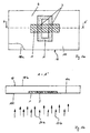
- FIG. 1a shows a carrier substrate 10 made of transparent PET, which has a prepared bottom 10 a.
- Figure 1 b shows the carrier substrate 10 from FIG. 1 a in section A - A '.
- the upper side of the carrier substrate 10 is designated by the reference numeral 10b.
- the underside 10a is provided in a first region 1 with a first diffractive relief structure and in a second region 2 with a second diffractive relief structure.
- the first and second relief structures are directly molded into the underside 10a of the carrier substrate, or the first and second relief structures are shaped into a replication lacquer layer provided on the underside.
- each of the first and second relief structures is a sine grid having a relief depth of 400 nm and a grating period of 350 nm, wherein the grating lines of the sine grating of the first relief structure are arranged substantially perpendicular to the grating lines of the sine grating of the second relief structure.
- Table 2 for such sine gratings a degree of transparency of 82.3% for the TE polarization direction and 62.8% for the TM polarization direction results.
- a relative difference in transparency of 30% results for the two different polarization directions.
- the azimuth angle of the first and second relief structure differs and the Depth-to-width ratio of the relief structure is preferably greater than 0.3.
- the relief structures exemplified in Table 2 with a grating period of 350 nm and a depth of 100 nm or 800 nm can be used, in which case the azimuth angle of the first and second relief structures preferably has an angular difference of approximately 90 °.
- a coating mask layer 100 of silver is sputtered over the entire surface in a constant area density with respect to the plane spanned by the carrier substrate 10.
- the first region 1 is so oriented for a according to the grid lines of the first relief structure, TE polarized light more transparent than the second region. Conversely, the second region is more transparent to the 90 ° polarized light than the first region.
- the third area in which a superposition of the first and second relief structure is provided (here cross-shaped sine grid with a depth of 400 nm and a grating period of 350 nm), the higher transmittance exists for both polarization directions.
- first exposure radiation 20a whose polarization direction is chosen so that the light is TE polarized with respect to the first relief structure
- second exposure radiation 20b which is an exposure to linearly polarized light having a wavelength of 550 nm and having a polarization direction rotated by 90 ° relative to the polarization direction of the exposure radiation 20a
- increased transmittance results in the second region 2 and third area 3.
- the exposure mask layer 100 is opaque and in a layer thickness, so that the fourth region 4 is impermeable to the first and the second exposure radiation 20a, 20b.
- Figure 1c shows the top 10b of the carrier substrate 10 from FIG. 1a upon exposure of the lower surface 10a to the first exposure radiation 20a.
- the exposure mask layer 100 has an increased permeability to the first exposure radiation 20a on the lower side 10a.
- Figure 1d shows the top 10b of the carrier substrate 10 from FIG. 1a upon exposure of the bottom 10a to the second exposure radiation 20b. Only in the second region 2 does the exposure mask layer 100 have an increased permeability for the second exposure radiation 20b on the underside 10a.
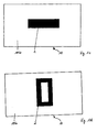
- FIG. 2a shows the carrier substrate 10 from FIG. 1a in section A - A 'with the first functional layer 30 of copper applied over its entire surface in a layer thickness of 0.1 .mu.m to 0.5 .mu.m and also a first negative photoresist layer 40 applied over the entire area.
- the first exposure radiation penetrates 20a amplifies in the first region 1 through the exposure mask layer 100, the carrier layer 10 and the first functional layer 30 and leads to a partially stronger exposure of the first photoresist layer 40.
- the exposure time and the exposure intensity are in this case matched to the photoresist used for the photoresist layer 40, that the photoresist is activated in the partially more exposed area 1, but is not activated in the less exposed areas 2 and 4.
- FIG. 2b shows the carrier substrate 10 from FIG. 2a after etching the first functional layer 30.
- the regions of the first functional layer 30 which were not covered by the etching mask were removed, so that a structured first functional layer 30 'was formed.
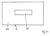
- Figure 2c shows the carrier substrate 10 from FIG. 2b after removal of the etching mask in plan view.
- the structured first functional layer 30 ' is present on the upper side 10a of the carrier substrate 10 in register with the first region 1 (see FIG. 1c) ,
- Figure 2d shows the carrier substrate 10 from Figure 2c in cross-section, with a third functional layer 50 of a transparent organic dielectric material applied over the entire area on the structured first functional layer 30 'and free areas of the carrier substrate 10.
- a second functional layer 31 made of copper in a layer thickness of 0.1 .mu.m to 0.5 .mu.m and a second positive photoresist layer 41 is also applied to the entire surface.
- the second exposure radiation 20b penetrates in the second region 2 through the exposure mask layer 100, the carrier layer 10, the first functional layer 30, the third functional layer 50 and the second functional layer 31, resulting in a partially stronger exposure of the second exposure beam 20b second photoresist layer 41.
- the exposure time and the exposure intensity are hereby adjusted to the photoresist used for the photoresist layer 41 such that the photoresist is in the partially more exposed area 2 is activated, but not activated in the less exposed areas 1 and 4.
- FIG. 2e shows the carrier substrate 10 from Figure 2d after development and structuring of the second photoresist layer or its remaining unexposed areas 41 ', and after etching of the second functional layer 31, wherein the structured second functional layer 31' was formed.
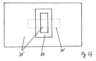
- FIG. 2f shows the carrier substrate 10 from FIG. 2e after removal of the structured second photoresist layer 41 'in plan view.
- the structured second functional layer 31 'on the third functional layer 50 can be seen.
- the position of the structured first functional layer 30 'below the third functional layer 50 is indicated by a dotted line.
- the structured first functional layer 30 ' is arranged in perfect register with the structured second functional layer 31'.
Landscapes
- Engineering & Computer Science (AREA)
- Manufacturing & Machinery (AREA)
- Exposure And Positioning Against Photoresist Photosensitive Materials (AREA)
- Electroluminescent Light Sources (AREA)
Claims (15)
- Procédé de fabrication d'un corps multicouche, en particulier d'un corps multicouche avec au moins un élément structurel électronique, le corps multicouche comportant au moins deux couches fonctionnelles, en particulier des couches fonctionnelles électriques, sur un côté supérieur (10b) d'un substrat porteur (10), qui sont structurées en alignement les unes par rapport aux autres,
caractérisé en ce
qu'un côté inférieur (10a) du substrat porteur (10) est préparé de telle manière qu'il résulte dans une première zone (1) une transparence accrue par rapport à au moins une seconde zone pour un premier rayonnement d'exposition (20a) et dans l'au moins une seconde zone (2) une transparence accrue par rapport à la première zone pour au moins un second rayonnement d'exposition (20) différent en alignement par rapport à la première zone (1), en ce que le côté inférieur (10a) est exposé successivement au premier et à l'au moins un second rayonnement d'exposition (20a, 20b) et en ce que le premier rayonnement d'exposition (20a) est utilisé pour la structuration d'une première couche fonctionnelle (30) et l'au moins un second rayonnement d'exposition (20b) pour la structuration d'au moins une seconde couche fonctionnelle (31) sur le côté supérieur (10b) du substrat porteur (10). - Procédé selon la revendication 1,
caractérisé en ce
que le côté inférieur (10a) du substrat porteur 10) est préparé en formant dans la première zone (1) une première structure en relief et dans la seconde zone (2) et en alignement par rapport à la première structure en relief, au moins une seconde structure en relief différente de la première structure en relief, en ce qu'une couche de masque d'exposition (100) est en outre appliquée sur le côté inférieur (10a), la couche de masque d'exposition (100) étant appliquée avec une densité superficielle constante par rapport à un plan défini par le substrat porteur (10), en ce que la première couche fonctionnelle (30) appliquée sur le côté supérieur (10b) du substrat porteur (10) est structurée en alignement par rapport à la première structure en relief et en ce que l'au moins une seconde couche fonctionnelle (31) électrique appliquée sur le côté supérieur (10b) du substrat porteur (10) est structurée en alignement par rapport à l'au moins une seconde structure en relief. - Procédé selon la revendication 2,
caractérisé en ce
que la couche de masque d'exposition (100) est formée par une couche métallique ou une couche en un alliage métallique. - Procédé selon l'une quelconque des revendications précédentes,
caractérisé en ce
que les première et seconde structures en relief sont formées par des structures en relief diffractives avec un rapport profondeur-largeur des éléments structurels individuels de ≥ 0,3. - Procédé selon l'une quelconque des revendications précédentes,
caractérisé en ce
que les première et seconde structures en relief sont formées par des structures en relief avec un pas de réseau ≤ 800 nm, de préférence ≤ 500 nm. - Procédé selon la revendication 1,
caractérisé en ce
que le côté inférieur (10a) du substrat porteur (10) est préparé en formant dans la première zone (1) une première structure en relief et dans la seconde zone (2) et en alignement par rapport à la première structure en relief, au moins une seconde structure en relief différente de la première structure en relief, en ce que la première couche fonctionnelle (30) appliquée sur le côté supérieur (10b) du substrat porteur (10) est structurée en alignement par rapport à la première structure en relief et en ce que l'au moins une seconde couche fonctionnelle (31) électrique appliquée sur le côté supérieur (10b) du substrat porteur (10) est structurée en alignement par rapport à l'au moins une seconde structure en relief. - Procédé selon la revendication 1,
caractérisé en ce
que le côté inférieur (10a) du substrat porteur (10) est préparé en disposant dans la première zone une première couche de couleur et dans la seconde zone et en alignement par rapport à la première couche de couleur, au moins une seconde couche de couleur dont la couleur est différente de celle de la première couche de couleur, et en ce que la première couche fonctionnelle appliquée sur le côté supérieur (10b) du substrat porteur (10) est structurée en alignement par rapport à la première couche de couleur et en ce que l'au moins une seconde couche fonctionnelle appliquée sur le côté supérieur (10b) du substrat porteur (10) est structurée en alignement par rapport à l'au moins une seconde couche de couleur. - Procédé selon l'une quelconque des revendications 1 à 7,
caractérisé en ce
que la première couche fonctionnelle (30') structurée est formée par un matériau de couche fonctionnelle électroconducteur. - Procédé selon l'une quelconque des revendications 1 à 8,
caractérisé en ce
que la seconde couche fonctionnelle (31') structurée est formée par un matériau de couche fonctionnelle électroconducteur ou semi-conducteur ou diélectrique. - Corps multicouche, en particulier corps multicouche avec au moins un élément structurel électronique organique qui présente un substrat porteur (10),
caractérisé en ce
qu'un côté inférieur (10a) du substrat porteur (10) est préparé en réalisant dans une première zone (1) une transparence accrue par rapport à au moins une seconde zone pour un premier rayonnement d'exposition (20a) et dans l'au moins une seconde zone (2) une transparence accrue par rapport à la première zone pour au moins un second rayonnement d'exposition différent (20b) et en ce que deux couches fonctionnelles (30', 31') structurées différemment sont disposées sur un côté supérieur (10b) du substrat porteur (10), dont une première couche fonctionnelle (30) est structurée de sorte que la première couche fonctionnelle (30') soit disposée en alignement par rapport à la première zone et une seconde couche fonctionnelle (31') étant structurée de sorte que la seconde couche fonctionnelle (31') soit disposée en alignement par rapport à la seconde zone (2). - Corps multicouche selon la revendication 10,
caractérisé en ce
qu'une première structure en relief est disposée dans la première zone (1) et au moins une seconde structure en relief différente de la première structure en relief est disposée dans la seconde zone (2) et en alignement par rapport à la première structure en relief. - Corps multicouche selon l'une quelconque des revendications 10 ou 11,
caractérisé en ce
qu'une couche de masque d'exposition (100) est en outre disposée sur le côté inférieur (10a). - Corps multicouche selon la revendication 12,
caractérisé en ce
qu'une première couche de couleur est disposée dans la première zone (1) et au moins une seconde couche de couleur dont la couleur est différente de celle de la première couche de couleur est disposée dans la seconde zone (2) et en alignement par rapport à la première couche de couleur. - Corps multicouche selon l'une quelconque des revendications 10 à 13,
caractérisé en ce
que le corps multicouche présente un ou plusieurs éléments structurels électriques, en particulier un condensateur, un transistor à effet de champ, une cellule solaire, un élément structurel contenant une couche photosensible, une résistance, une antenne, une LED, en particulier une OLED ou une diode. - Corps multicouche selon l'une quelconque des revendications 10 à 14,
caractérisé en ce
que le corps multicouche présente comme substrat une couche de verre, et en ce que le corps multicouche présente dans la zone du côté inférieur une couche de laque de réplique, dans laquelle une première structure en relief diffractive est moulée dans la première zone, et dans laquelle une seconde structure en relief différente est moulée dans l'au moins une autre seconde zone.
Applications Claiming Priority (2)
| Application Number | Priority Date | Filing Date | Title |
|---|---|---|---|
| DE102006037433A DE102006037433B4 (de) | 2006-08-09 | 2006-08-09 | Verfahren zur Herstellung eines Mehrschichtkörpers sowie Mehrschichtkörper |
| PCT/EP2007/006884 WO2008017426A1 (fr) | 2006-08-09 | 2007-08-03 | Procédé de fabrication d'au moins un corps multicouche et corps multicouche |
Publications (2)
| Publication Number | Publication Date |
|---|---|
| EP2050150A1 EP2050150A1 (fr) | 2009-04-22 |
| EP2050150B1 true EP2050150B1 (fr) | 2013-04-24 |
Family
ID=38608712
Family Applications (1)
| Application Number | Title | Priority Date | Filing Date |
|---|---|---|---|
| EP07801506.2A Not-in-force EP2050150B1 (fr) | 2006-08-09 | 2007-08-03 | Procédé de fabrication d'au moins un corps multicouche et corps multicouche |
Country Status (6)
| Country | Link |
|---|---|
| US (2) | US8129217B2 (fr) |
| EP (1) | EP2050150B1 (fr) |
| JP (1) | JP4944200B2 (fr) |
| DE (1) | DE102006037433B4 (fr) |
| DK (1) | DK2050150T3 (fr) |
| WO (1) | WO2008017426A1 (fr) |
Families Citing this family (30)
| Publication number | Priority date | Publication date | Assignee | Title |
|---|---|---|---|---|
| CN102097458B (zh) | 2004-06-04 | 2013-10-30 | 伊利诺伊大学评议会 | 用于制造并组装可印刷半导体元件的方法和设备 |
| US7799699B2 (en) | 2004-06-04 | 2010-09-21 | The Board Of Trustees Of The University Of Illinois | Printable semiconductor structures and related methods of making and assembling |
| WO2008036837A2 (fr) * | 2006-09-20 | 2008-03-27 | The Board Of Trustees Of The University Of Illinois | Strategies de liberation mises en œuvre dans la fabrication de structures semiconductrices transferables, de dispositifs et de composants de dispositifs |
| EP2104954B1 (fr) | 2007-01-17 | 2022-03-16 | The Board of Trustees of the University of Illinois | Systèmes optiques fabriqués par un ensemble à base d'impression |
| US8372726B2 (en) | 2008-10-07 | 2013-02-12 | Mc10, Inc. | Methods and applications of non-planar imaging arrays |
| US8389862B2 (en) | 2008-10-07 | 2013-03-05 | Mc10, Inc. | Extremely stretchable electronics |
| US8097926B2 (en) | 2008-10-07 | 2012-01-17 | Mc10, Inc. | Systems, methods, and devices having stretchable integrated circuitry for sensing and delivering therapy |
| EP2349440B1 (fr) | 2008-10-07 | 2019-08-21 | Mc10, Inc. | Ballonnet de cathéter comportant un circuit intégré étirable et un réseau de détecteurs |
| US8886334B2 (en) | 2008-10-07 | 2014-11-11 | Mc10, Inc. | Systems, methods, and devices using stretchable or flexible electronics for medical applications |
| RU2573160C2 (ru) * | 2009-03-30 | 2016-01-20 | Боэгли-Гравюр С.А. | Способ и устройство для структурирования поверхности твердого тела покрытого твердым материалом, с помощью лазера |
| CA2756840C (fr) | 2009-03-30 | 2018-10-23 | Boegli-Gravures S.A. | Procede et dispositif de structuration d'une surface de corps solide par revetement dur au moyen d'un laser |
| WO2010132552A1 (fr) | 2009-05-12 | 2010-11-18 | The Board Of Trustees Of The University Of Illinois | Ensembles imprimés de diodes électroluminescentes inorganiques microscopiques ultraminces pour dispositifs d'affichage déformables et semi-transparents |
| US9723122B2 (en) | 2009-10-01 | 2017-08-01 | Mc10, Inc. | Protective cases with integrated electronics |
| US10918298B2 (en) | 2009-12-16 | 2021-02-16 | The Board Of Trustees Of The University Of Illinois | High-speed, high-resolution electrophysiology in-vivo using conformal electronics |
| US10441185B2 (en) | 2009-12-16 | 2019-10-15 | The Board Of Trustees Of The University Of Illinois | Flexible and stretchable electronic systems for epidermal electronics |
| US9936574B2 (en) | 2009-12-16 | 2018-04-03 | The Board Of Trustees Of The University Of Illinois | Waterproof stretchable optoelectronics |
| CN102892356B (zh) | 2010-03-17 | 2016-01-13 | 伊利诺伊大学评议会 | 基于生物可吸收基质的可植入生物医学装置 |
| US9442285B2 (en) | 2011-01-14 | 2016-09-13 | The Board Of Trustees Of The University Of Illinois | Optical component array having adjustable curvature |
| CN103348503A (zh) * | 2011-03-03 | 2013-10-09 | 正交公司 | 薄膜器件的材料图案化工艺 |
| WO2012158709A1 (fr) | 2011-05-16 | 2012-11-22 | The Board Of Trustees Of The University Of Illinois | Barrettes de del à gestion thermique assemblées par impression |
| JP2014523633A (ja) | 2011-05-27 | 2014-09-11 | エムシー10 インコーポレイテッド | 電子的、光学的、且つ/又は機械的装置及びシステム並びにこれらの装置及びシステムを製造する方法 |
| WO2012167096A2 (fr) | 2011-06-03 | 2012-12-06 | The Board Of Trustees Of The University Of Illinois | Réseau d'électrodes de surface conformables, multiplexées de manière active et à haute densité, pour un interfaçage avec le cerveau |
| EP2786644B1 (fr) | 2011-12-01 | 2019-04-10 | The Board of Trustees of the University of Illionis | Dispositifs transitoires conçus pour subir des transformations programmables |
| JP2015521303A (ja) | 2012-03-30 | 2015-07-27 | ザ ボード オブ トラスティーズ オブ ザ ユニヴァーシ | 表面への形状適合可能な付属物装着可能電子デバイス |
| DE102012108170B4 (de) * | 2012-09-03 | 2015-01-22 | Bundesdruckerei Gmbh | Sicherheitselement und Verfahren zur Herstellung eines Sicherheitselements |
| US9171794B2 (en) | 2012-10-09 | 2015-10-27 | Mc10, Inc. | Embedding thin chips in polymer |
| JP2018524677A (ja) | 2015-06-01 | 2018-08-30 | ザ ボード オブ トラスティーズ オブ ザ ユニヴァーシティー オブ イリノイ | 無線電力及び近距離無線通信機能を備えた小型電子システム |
| KR20180034342A (ko) | 2015-06-01 | 2018-04-04 | 더 보드 오브 트러스티즈 오브 더 유니버시티 오브 일리노이 | 대안적인 자외선 감지방법 |
| US10925543B2 (en) | 2015-11-11 | 2021-02-23 | The Board Of Trustees Of The University Of Illinois | Bioresorbable silicon electronics for transient implants |
| EP3985715A4 (fr) * | 2020-06-01 | 2022-11-09 | Changxin Memory Technologies, Inc. | Procédé de conception d'agencement de tranche et système d'exposition de machine de lithographie |
Citations (5)
| Publication number | Priority date | Publication date | Assignee | Title |
|---|---|---|---|---|
| US3829213A (en) * | 1972-06-02 | 1974-08-13 | Mos Technology Inc | Artproof method for semiconductor devices |
| EP0673045A1 (fr) * | 1994-03-11 | 1995-09-20 | Dow Corning S.A. | Feuilles pour un condensateur multicouche |
| US20020195928A1 (en) * | 2001-06-25 | 2002-12-26 | Grace Anthony J. | Electroluminescent display device and method of making |
| WO2005039868A2 (fr) * | 2003-10-24 | 2005-05-06 | Leonhard Kurz Gmbh & Co. Kg | Procede de production d'un film |
| DE102004059798A1 (de) * | 2004-12-10 | 2006-06-29 | Ovd Kinegram Ag | Optisch variables Element mit elektrisch aktiver Schicht |
Family Cites Families (12)
| Publication number | Priority date | Publication date | Assignee | Title |
|---|---|---|---|---|
| US4374911A (en) * | 1978-04-28 | 1983-02-22 | International Business Machines Corporation | Photo method of making tri-level density photomask |
| US5932397A (en) * | 1996-05-28 | 1999-08-03 | Rvm Scientific, Inc. | Multicolor lithography for control of three dimensional refractive index gradient processing |
| US6133933A (en) * | 1997-01-13 | 2000-10-17 | Xerox Corporation | Color Xerographic printing system with multicolor printbar |
| US6255130B1 (en) * | 1998-11-19 | 2001-07-03 | Samsung Electronics Co., Ltd. | Thin film transistor array panel and a method for manufacturing the same |
| CA2389347A1 (fr) * | 1999-12-02 | 2001-06-07 | Tony C. Kowalczyk | Photodefinition de dispositifs optiques |
| US6569580B2 (en) * | 2001-03-13 | 2003-05-27 | Diverging Technologies, Inc. | Binary and phase-shift photomasks |
| US7160649B2 (en) * | 2002-07-11 | 2007-01-09 | Hitachi Via Mechanics, Ltd. | Gray level imaging masks, optical imaging apparatus for gray level imaging masks and methods for encoding mask and use of the masks |
| KR20050109963A (ko) * | 2003-03-07 | 2005-11-22 | 코닌클리케 필립스 일렉트로닉스 엔.브이. | 전자 장치 제조 방법 |
| JP3746497B2 (ja) | 2003-06-24 | 2006-02-15 | 松下電器産業株式会社 | フォトマスク |
| DE102004059467A1 (de) * | 2004-12-10 | 2006-07-20 | Polyic Gmbh & Co. Kg | Gatter aus organischen Feldeffekttransistoren |
| JP4769544B2 (ja) * | 2005-10-28 | 2011-09-07 | Hoya株式会社 | 二次鋳型の製造方法 |
| US8906490B2 (en) * | 2006-05-19 | 2014-12-09 | Eastman Kodak Company | Multicolor mask |
-
2006
- 2006-08-09 DE DE102006037433A patent/DE102006037433B4/de not_active Expired - Fee Related
-
2007
- 2007-08-03 EP EP07801506.2A patent/EP2050150B1/fr not_active Not-in-force
- 2007-08-03 US US12/309,908 patent/US8129217B2/en not_active Expired - Fee Related
- 2007-08-03 JP JP2009523184A patent/JP4944200B2/ja not_active Expired - Fee Related
- 2007-08-03 WO PCT/EP2007/006884 patent/WO2008017426A1/fr active Application Filing
- 2007-08-03 DK DK07801506.2T patent/DK2050150T3/da active
-
2012
- 2012-01-25 US US13/358,007 patent/US8502213B2/en not_active Expired - Fee Related
Patent Citations (5)
| Publication number | Priority date | Publication date | Assignee | Title |
|---|---|---|---|---|
| US3829213A (en) * | 1972-06-02 | 1974-08-13 | Mos Technology Inc | Artproof method for semiconductor devices |
| EP0673045A1 (fr) * | 1994-03-11 | 1995-09-20 | Dow Corning S.A. | Feuilles pour un condensateur multicouche |
| US20020195928A1 (en) * | 2001-06-25 | 2002-12-26 | Grace Anthony J. | Electroluminescent display device and method of making |
| WO2005039868A2 (fr) * | 2003-10-24 | 2005-05-06 | Leonhard Kurz Gmbh & Co. Kg | Procede de production d'un film |
| DE102004059798A1 (de) * | 2004-12-10 | 2006-06-29 | Ovd Kinegram Ag | Optisch variables Element mit elektrisch aktiver Schicht |
Non-Patent Citations (4)
| Title |
|---|
| "Fabricating Printed Circuit Boards", 1 January 2002, ELSEVIER SCIENCE (USA), ISBN: 978-1-87-870750-5, article JON VARTERESIAN: "Making Printed Circuit Boards", pages: 69 - 72, XP055042087 * |
| A. HÜBLER: "Funktionale Polymere - Gedruckte Elektronik als Chance", DEGUSSA SCIENCENEWSLETTER, ELEMENTS, vol. 13, 2005, pages 10 - 13 * |
| HELMUT KIPPHAN: "Handbook of Print Media", 2000, SPRINGER VERLAG, ISBN: 3-540-66941-8, pages: 1164 * |
| Vortragsunterlagen von Prof. Dr. Arved Hübler, "Printing Technologies for Polytronic Structures", 1st Polyscene Workshop at IMEC in Leuven, Belgium * |
Also Published As
| Publication number | Publication date |
|---|---|
| JP4944200B2 (ja) | 2012-05-30 |
| DK2050150T3 (da) | 2013-07-22 |
| US8129217B2 (en) | 2012-03-06 |
| WO2008017426A1 (fr) | 2008-02-14 |
| EP2050150A1 (fr) | 2009-04-22 |
| US8502213B2 (en) | 2013-08-06 |
| JP2010500606A (ja) | 2010-01-07 |
| DE102006037433B4 (de) | 2010-08-19 |
| US20120164391A1 (en) | 2012-06-28 |
| DE102006037433A1 (de) | 2008-02-28 |
| US20090289246A1 (en) | 2009-11-26 |
Similar Documents
| Publication | Publication Date | Title |
|---|---|---|
| EP2050150B1 (fr) | Procédé de fabrication d'au moins un corps multicouche et corps multicouche | |
| DE102005006277B4 (de) | Verfahren zur Herstellung eines Mehrschichtkörpers | |
| DE102006039071B4 (de) | Optisches Filter und Verfahren zu seiner Herstellung | |
| DE69326745T2 (de) | Lichtsteuerelement für hochauflösende optische systeme und verfahren zu seiner herstellung | |
| DE102005006231B4 (de) | Verfahren zur Herstellung eines Mehrschichtkörpers | |
| EP1937471B1 (fr) | Corps multicouche et procede de realisation | |
| DE69914956T2 (de) | Thermotransfer einer russ enthaltenden schwarzen matrix | |
| DE102007060108B4 (de) | Verfahren zur Herstellung eines Solarzellenmoduls | |
| DE102008013073B4 (de) | Verfahren zur Herstellung eines Folienelements und Folienelement | |
| DE102011115125B4 (de) | Herstellung einer mikrooptischen Darstellungsanordnung | |
| EP1785016B1 (fr) | Corps multicouche ayant des zones de differentes microstructurations dotees d'un revetement electroconducteur | |
| EP1559147B1 (fr) | Feuille contenant des semi-conducteurs organiques | |
| DE102010019766A1 (de) | Verfahren zur Erzeugung einer Mikrostruktur auf einem Träger | |
| DE112016002084T5 (de) | Berührungssensor, der mit einer Zirkular-Polarisationsplatte versehen ist, und Bildanzeigevorrichtung | |
| DE102005002837A1 (de) | Verfahren zur Herstellung einer Elektrode | |
| EP1599344B1 (fr) | Element de securite | |
| DE102009051887A1 (de) | Verfahren zur Ausbildung einer Mikrolinse eines Bildsensors und Verfahren zur Herstellung des Bildsensors | |
| EP3302997B1 (fr) | Procédé de fabrication d'un élément de sécurité, élément de sécurité, papier de sécurité et document de valeur obtenables par ce procédé | |
| DE102004002024A1 (de) | Organischer Transistor mit selbstjustierender Gate-Elektrode und Verfahren zu dessen Herstellung | |
| DE102006035749A1 (de) | Verfahren zur Herstellung mindestens eines Bauteils sowie Bauteil | |
| DE20020604U1 (de) | Vorrichtung zur Herstellung eines halbleitenden und/oder Elektrolumineszenz zeigenden organischen Schichtaufbaus |
Legal Events
| Date | Code | Title | Description |
|---|---|---|---|
| PUAI | Public reference made under article 153(3) epc to a published international application that has entered the european phase |
Free format text: ORIGINAL CODE: 0009012 |
|
| 17P | Request for examination filed |
Effective date: 20090116 |
|
| AK | Designated contracting states |
Kind code of ref document: A1 Designated state(s): AT BE BG CH CY CZ DE DK EE ES FI FR GB GR HU IE IS IT LI LT LU LV MC MT NL PL PT RO SE SI SK TR |
|
| AX | Request for extension of the european patent |
Extension state: AL BA HR MK RS |
|
| 17Q | First examination report despatched |
Effective date: 20100608 |
|
| DAX | Request for extension of the european patent (deleted) | ||
| GRAP | Despatch of communication of intention to grant a patent |
Free format text: ORIGINAL CODE: EPIDOSNIGR1 |
|
| RIC1 | Information provided on ipc code assigned before grant |
Ipc: G03F 1/00 20120101ALI20130107BHEP Ipc: H01L 51/00 20060101AFI20130107BHEP |
|
| GRAS | Grant fee paid |
Free format text: ORIGINAL CODE: EPIDOSNIGR3 |
|
| GRAA | (expected) grant |
Free format text: ORIGINAL CODE: 0009210 |
|
| AK | Designated contracting states |
Kind code of ref document: B1 Designated state(s): AT BE BG CH CY CZ DE DK EE ES FI FR GB GR HU IE IS IT LI LT LU LV MC MT NL PL PT RO SE SI SK TR |
|
| REG | Reference to a national code |
Ref country code: GB Ref legal event code: FG4D Free format text: NOT ENGLISH |
|
| REG | Reference to a national code |
Ref country code: CH Ref legal event code: EP |
|
| REG | Reference to a national code |
Ref country code: AT Ref legal event code: REF Ref document number: 609082 Country of ref document: AT Kind code of ref document: T Effective date: 20130515 Ref country code: CH Ref legal event code: NV Representative=s name: FIAMMENGHI-FIAMMENGHI, CH |
|
| REG | Reference to a national code |
Ref country code: IE Ref legal event code: FG4D Free format text: LANGUAGE OF EP DOCUMENT: GERMAN |
|
| REG | Reference to a national code |
Ref country code: DE Ref legal event code: R096 Ref document number: 502007011664 Country of ref document: DE Effective date: 20130620 |
|
| REG | Reference to a national code |
Ref country code: DK Ref legal event code: T3 |
|
| REG | Reference to a national code |
Ref country code: SE Ref legal event code: TRGR |
|
| REG | Reference to a national code |
Ref country code: NL Ref legal event code: T3 |
|
| REG | Reference to a national code |
Ref country code: LT Ref legal event code: MG4D |
|
| PG25 | Lapsed in a contracting state [announced via postgrant information from national office to epo] |
Ref country code: PT Free format text: LAPSE BECAUSE OF FAILURE TO SUBMIT A TRANSLATION OF THE DESCRIPTION OR TO PAY THE FEE WITHIN THE PRESCRIBED TIME-LIMIT Effective date: 20130826 Ref country code: GR Free format text: LAPSE BECAUSE OF FAILURE TO SUBMIT A TRANSLATION OF THE DESCRIPTION OR TO PAY THE FEE WITHIN THE PRESCRIBED TIME-LIMIT Effective date: 20130725 Ref country code: LT Free format text: LAPSE BECAUSE OF FAILURE TO SUBMIT A TRANSLATION OF THE DESCRIPTION OR TO PAY THE FEE WITHIN THE PRESCRIBED TIME-LIMIT Effective date: 20130424 Ref country code: IS Free format text: LAPSE BECAUSE OF FAILURE TO SUBMIT A TRANSLATION OF THE DESCRIPTION OR TO PAY THE FEE WITHIN THE PRESCRIBED TIME-LIMIT Effective date: 20130824 Ref country code: SI Free format text: LAPSE BECAUSE OF FAILURE TO SUBMIT A TRANSLATION OF THE DESCRIPTION OR TO PAY THE FEE WITHIN THE PRESCRIBED TIME-LIMIT Effective date: 20130424 Ref country code: ES Free format text: LAPSE BECAUSE OF FAILURE TO SUBMIT A TRANSLATION OF THE DESCRIPTION OR TO PAY THE FEE WITHIN THE PRESCRIBED TIME-LIMIT Effective date: 20130804 |
|
| PG25 | Lapsed in a contracting state [announced via postgrant information from national office to epo] |
Ref country code: BG Free format text: LAPSE BECAUSE OF FAILURE TO SUBMIT A TRANSLATION OF THE DESCRIPTION OR TO PAY THE FEE WITHIN THE PRESCRIBED TIME-LIMIT Effective date: 20130724 Ref country code: LV Free format text: LAPSE BECAUSE OF FAILURE TO SUBMIT A TRANSLATION OF THE DESCRIPTION OR TO PAY THE FEE WITHIN THE PRESCRIBED TIME-LIMIT Effective date: 20130424 Ref country code: PL Free format text: LAPSE BECAUSE OF FAILURE TO SUBMIT A TRANSLATION OF THE DESCRIPTION OR TO PAY THE FEE WITHIN THE PRESCRIBED TIME-LIMIT Effective date: 20130424 Ref country code: CY Free format text: LAPSE BECAUSE OF FAILURE TO SUBMIT A TRANSLATION OF THE DESCRIPTION OR TO PAY THE FEE WITHIN THE PRESCRIBED TIME-LIMIT Effective date: 20130424 |
|
| PG25 | Lapsed in a contracting state [announced via postgrant information from national office to epo] |
Ref country code: EE Free format text: LAPSE BECAUSE OF FAILURE TO SUBMIT A TRANSLATION OF THE DESCRIPTION OR TO PAY THE FEE WITHIN THE PRESCRIBED TIME-LIMIT Effective date: 20130424 Ref country code: SK Free format text: LAPSE BECAUSE OF FAILURE TO SUBMIT A TRANSLATION OF THE DESCRIPTION OR TO PAY THE FEE WITHIN THE PRESCRIBED TIME-LIMIT Effective date: 20130424 Ref country code: CZ Free format text: LAPSE BECAUSE OF FAILURE TO SUBMIT A TRANSLATION OF THE DESCRIPTION OR TO PAY THE FEE WITHIN THE PRESCRIBED TIME-LIMIT Effective date: 20130424 |
|
| BERE | Be: lapsed |
Owner name: OVD KINEGRAM A.G. Effective date: 20130831 |
|
| PG25 | Lapsed in a contracting state [announced via postgrant information from national office to epo] |
Ref country code: RO Free format text: LAPSE BECAUSE OF FAILURE TO SUBMIT A TRANSLATION OF THE DESCRIPTION OR TO PAY THE FEE WITHIN THE PRESCRIBED TIME-LIMIT Effective date: 20130424 |
|
| PLBE | No opposition filed within time limit |
Free format text: ORIGINAL CODE: 0009261 |
|
| STAA | Information on the status of an ep patent application or granted ep patent |
Free format text: STATUS: NO OPPOSITION FILED WITHIN TIME LIMIT |
|
| 26N | No opposition filed |
Effective date: 20140127 |
|
| PG25 | Lapsed in a contracting state [announced via postgrant information from national office to epo] |
Ref country code: MC Free format text: LAPSE BECAUSE OF FAILURE TO SUBMIT A TRANSLATION OF THE DESCRIPTION OR TO PAY THE FEE WITHIN THE PRESCRIBED TIME-LIMIT Effective date: 20130424 |
|
| REG | Reference to a national code |
Ref country code: DE Ref legal event code: R097 Ref document number: 502007011664 Country of ref document: DE Effective date: 20140127 |
|
| REG | Reference to a national code |
Ref country code: IE Ref legal event code: MM4A |
|
| PG25 | Lapsed in a contracting state [announced via postgrant information from national office to epo] |
Ref country code: BE Free format text: LAPSE BECAUSE OF NON-PAYMENT OF DUE FEES Effective date: 20130831 |
|
| PG25 | Lapsed in a contracting state [announced via postgrant information from national office to epo] |
Ref country code: IE Free format text: LAPSE BECAUSE OF NON-PAYMENT OF DUE FEES Effective date: 20130803 |
|
| REG | Reference to a national code |
Ref country code: AT Ref legal event code: MM01 Ref document number: 609082 Country of ref document: AT Kind code of ref document: T Effective date: 20130803 |
|
| PG25 | Lapsed in a contracting state [announced via postgrant information from national office to epo] |
Ref country code: AT Free format text: LAPSE BECAUSE OF NON-PAYMENT OF DUE FEES Effective date: 20130803 |
|
| PG25 | Lapsed in a contracting state [announced via postgrant information from national office to epo] |
Ref country code: MT Free format text: LAPSE BECAUSE OF FAILURE TO SUBMIT A TRANSLATION OF THE DESCRIPTION OR TO PAY THE FEE WITHIN THE PRESCRIBED TIME-LIMIT Effective date: 20130424 |
|
| PG25 | Lapsed in a contracting state [announced via postgrant information from national office to epo] |
Ref country code: HU Free format text: LAPSE BECAUSE OF FAILURE TO SUBMIT A TRANSLATION OF THE DESCRIPTION OR TO PAY THE FEE WITHIN THE PRESCRIBED TIME-LIMIT; INVALID AB INITIO Effective date: 20070803 Ref country code: LU Free format text: LAPSE BECAUSE OF NON-PAYMENT OF DUE FEES Effective date: 20130803 |
|
| REG | Reference to a national code |
Ref country code: FR Ref legal event code: PLFP Year of fee payment: 10 |
|
| REG | Reference to a national code |
Ref country code: FR Ref legal event code: PLFP Year of fee payment: 11 |
|
| REG | Reference to a national code |
Ref country code: FR Ref legal event code: PLFP Year of fee payment: 12 |
|
| PGFP | Annual fee paid to national office [announced via postgrant information from national office to epo] |
Ref country code: NL Payment date: 20190821 Year of fee payment: 13 |
|
| PGFP | Annual fee paid to national office [announced via postgrant information from national office to epo] |
Ref country code: FR Payment date: 20190822 Year of fee payment: 13 Ref country code: DK Payment date: 20190822 Year of fee payment: 13 Ref country code: FI Payment date: 20190820 Year of fee payment: 13 Ref country code: IT Payment date: 20190821 Year of fee payment: 13 Ref country code: SE Payment date: 20190826 Year of fee payment: 13 Ref country code: TR Payment date: 20190726 Year of fee payment: 13 Ref country code: DE Payment date: 20190705 Year of fee payment: 13 |
|
| PGFP | Annual fee paid to national office [announced via postgrant information from national office to epo] |
Ref country code: GB Payment date: 20190827 Year of fee payment: 13 |
|
| PGFP | Annual fee paid to national office [announced via postgrant information from national office to epo] |
Ref country code: CH Payment date: 20190826 Year of fee payment: 13 |
|
| REG | Reference to a national code |
Ref country code: DE Ref legal event code: R119 Ref document number: 502007011664 Country of ref document: DE |
|
| REG | Reference to a national code |
Ref country code: FI Ref legal event code: MAE |
|
| REG | Reference to a national code |
Ref country code: DK Ref legal event code: EBP Effective date: 20200831 |
|
| REG | Reference to a national code |
Ref country code: SE Ref legal event code: EUG |
|
| REG | Reference to a national code |
Ref country code: CH Ref legal event code: PL |
|
| REG | Reference to a national code |
Ref country code: NL Ref legal event code: MM Effective date: 20200901 |
|
| GBPC | Gb: european patent ceased through non-payment of renewal fee |
Effective date: 20200803 |
|
| PG25 | Lapsed in a contracting state [announced via postgrant information from national office to epo] |
Ref country code: FI Free format text: LAPSE BECAUSE OF NON-PAYMENT OF DUE FEES Effective date: 20200803 Ref country code: LI Free format text: LAPSE BECAUSE OF NON-PAYMENT OF DUE FEES Effective date: 20200831 Ref country code: CH Free format text: LAPSE BECAUSE OF NON-PAYMENT OF DUE FEES Effective date: 20200831 |
|
| PG25 | Lapsed in a contracting state [announced via postgrant information from national office to epo] |
Ref country code: SE Free format text: LAPSE BECAUSE OF NON-PAYMENT OF DUE FEES Effective date: 20200804 |
|
| PG25 | Lapsed in a contracting state [announced via postgrant information from national office to epo] |
Ref country code: DE Free format text: LAPSE BECAUSE OF NON-PAYMENT OF DUE FEES Effective date: 20210302 Ref country code: IT Free format text: LAPSE BECAUSE OF NON-PAYMENT OF DUE FEES Effective date: 20200803 Ref country code: FR Free format text: LAPSE BECAUSE OF NON-PAYMENT OF DUE FEES Effective date: 20200831 |
|
| PG25 | Lapsed in a contracting state [announced via postgrant information from national office to epo] |
Ref country code: DK Free format text: LAPSE BECAUSE OF NON-PAYMENT OF DUE FEES Effective date: 20200831 Ref country code: GB Free format text: LAPSE BECAUSE OF NON-PAYMENT OF DUE FEES Effective date: 20200803 |
|
| PG25 | Lapsed in a contracting state [announced via postgrant information from national office to epo] |
Ref country code: NL Free format text: LAPSE BECAUSE OF NON-PAYMENT OF DUE FEES Effective date: 20200901 |
|
| PG25 | Lapsed in a contracting state [announced via postgrant information from national office to epo] |
Ref country code: TR Free format text: LAPSE BECAUSE OF NON-PAYMENT OF DUE FEES Effective date: 20200803 |