EP2050150B1 - Method for producing at least one multilayer body, and multilayer body - Google Patents
Method for producing at least one multilayer body, and multilayer body Download PDFInfo
- Publication number
- EP2050150B1 EP2050150B1 EP07801506.2A EP07801506A EP2050150B1 EP 2050150 B1 EP2050150 B1 EP 2050150B1 EP 07801506 A EP07801506 A EP 07801506A EP 2050150 B1 EP2050150 B1 EP 2050150B1
- Authority
- EP
- European Patent Office
- Prior art keywords
- layer
- region
- carrier substrate
- relief structure
- functional layer
- Prior art date
- Legal status (The legal status is an assumption and is not a legal conclusion. Google has not performed a legal analysis and makes no representation as to the accuracy of the status listed.)
- Not-in-force
Links
Images


Classifications
-
- H—ELECTRICITY
- H10—SEMICONDUCTOR DEVICES; ELECTRIC SOLID-STATE DEVICES NOT OTHERWISE PROVIDED FOR
- H10K—ORGANIC ELECTRIC SOLID-STATE DEVICES
- H10K71/00—Manufacture or treatment specially adapted for the organic devices covered by this subclass
- H10K71/20—Changing the shape of the active layer in the devices, e.g. patterning
- H10K71/231—Changing the shape of the active layer in the devices, e.g. patterning by etching of existing layers
- H10K71/233—Changing the shape of the active layer in the devices, e.g. patterning by etching of existing layers by photolithographic etching
-
- H—ELECTRICITY
- H10—SEMICONDUCTOR DEVICES; ELECTRIC SOLID-STATE DEVICES NOT OTHERWISE PROVIDED FOR
- H10K—ORGANIC ELECTRIC SOLID-STATE DEVICES
- H10K10/00—Organic devices specially adapted for rectifying, amplifying, oscillating or switching; Organic capacitors or resistors having a potential-jump barrier or a surface barrier
- H10K10/40—Organic transistors
- H10K10/46—Field-effect transistors, e.g. organic thin-film transistors [OTFT]
- H10K10/462—Insulated gate field-effect transistors [IGFETs]
- H10K10/464—Lateral top-gate IGFETs comprising only a single gate
-
- Y—GENERAL TAGGING OF NEW TECHNOLOGICAL DEVELOPMENTS; GENERAL TAGGING OF CROSS-SECTIONAL TECHNOLOGIES SPANNING OVER SEVERAL SECTIONS OF THE IPC; TECHNICAL SUBJECTS COVERED BY FORMER USPC CROSS-REFERENCE ART COLLECTIONS [XRACs] AND DIGESTS
- Y02—TECHNOLOGIES OR APPLICATIONS FOR MITIGATION OR ADAPTATION AGAINST CLIMATE CHANGE
- Y02E—REDUCTION OF GREENHOUSE GAS [GHG] EMISSIONS, RELATED TO ENERGY GENERATION, TRANSMISSION OR DISTRIBUTION
- Y02E10/00—Energy generation through renewable energy sources
- Y02E10/50—Photovoltaic [PV] energy
- Y02E10/549—Organic PV cells
-
- Y—GENERAL TAGGING OF NEW TECHNOLOGICAL DEVELOPMENTS; GENERAL TAGGING OF CROSS-SECTIONAL TECHNOLOGIES SPANNING OVER SEVERAL SECTIONS OF THE IPC; TECHNICAL SUBJECTS COVERED BY FORMER USPC CROSS-REFERENCE ART COLLECTIONS [XRACs] AND DIGESTS
- Y10—TECHNICAL SUBJECTS COVERED BY FORMER USPC
- Y10T—TECHNICAL SUBJECTS COVERED BY FORMER US CLASSIFICATION
- Y10T428/00—Stock material or miscellaneous articles
- Y10T428/24—Structurally defined web or sheet [e.g., overall dimension, etc.]
- Y10T428/24479—Structurally defined web or sheet [e.g., overall dimension, etc.] including variation in thickness
- Y10T428/24612—Composite web or sheet
-
- Y—GENERAL TAGGING OF NEW TECHNOLOGICAL DEVELOPMENTS; GENERAL TAGGING OF CROSS-SECTIONAL TECHNOLOGIES SPANNING OVER SEVERAL SECTIONS OF THE IPC; TECHNICAL SUBJECTS COVERED BY FORMER USPC CROSS-REFERENCE ART COLLECTIONS [XRACs] AND DIGESTS
- Y10—TECHNICAL SUBJECTS COVERED BY FORMER USPC
- Y10T—TECHNICAL SUBJECTS COVERED BY FORMER US CLASSIFICATION
- Y10T428/00—Stock material or miscellaneous articles
- Y10T428/24—Structurally defined web or sheet [e.g., overall dimension, etc.]
- Y10T428/24802—Discontinuous or differential coating, impregnation or bond [e.g., artwork, printing, retouched photograph, etc.]
Definitions
- the invention relates to a method for producing a multilayer body, in particular a multilayer body having at least one electronic component, wherein the multilayer body comprises at least two functional layers, in particular electrical functional layers, on an upper side of a carrier substrate, which are structured in register with one another.
- the invention further relates to a multi-layer body obtainable thereafter.
- OFET organic field effect transistors
- the field-effect transistors are formed from a plurality of functional layers or functional layers, which are applied to the carrier substrate, in particular by printing or knife coating.
- the carrier substrate is formed inter alia as a plastic film with a thickness in the range of 6 to 200 microns.
- Thick support substrates have heretofore been preferred because processing of thinner, less costly support substrates having a thickness in the range of 6 to about 50 microns has been found to be prone to distortion during processing, with the distortion varying with each processing step. If an electrical functional layer is applied and patterned on the thin carrier substrate, a noticeable distortion or perpendicular to the carrier substrate already results in a deviation of the shape of the functional layer from its ideal shape. The delay has a particularly disturbing effect if, subsequently or after application of one or more full-surface functional layers, combined with a further change in the dimensions of the already formed structured functional layer, a further structured functional layer must be arranged in the register relative to the already formed structured functional layer.
- the object is achieved for the method for producing a multilayer body, which comprises at least two, in particular electrically functional layers on an upper side of a carrier substrate, which are structured in register to each other, that a bottom of the carrier substrate is prepared such that in a first region, a permeability for a first exposure radiation and in at least one second region, a transmission for at least one different second exposure radiation in the register to the first region results in that the bottom is successively exposed to the first and the at least one second exposure radiation, and that the first exposure radiation for structuring a first functional layer and the at least one second exposure radiation is used for structuring at least one second functional layer on the upper side of the carrier substrate.
- the method according to the invention makes possible an unproblematic arrangement of the at least one second functional layer in the perfect or nearly perfect register to the first functional layer, since the distortion occurring equally affects the first region and the at least one second region.
- the shape of the first region is changed perpendicular to the plane of the carrier substrate in accordance with the shape of the at least one second region by the distortion, so that the position of the first region with respect to the position of the at least one second region can not shift.
- the position of the first region and of the at least one second region is thus already established on the carrier substrate at the beginning of the production process, so that an inaccuracy in the orientation of the first functional layer relative to the at least one second functional layer can no longer occur despite a distortion of the carrier substrate.
- the at least one second functional layer is formed in a position that is different from its ideal shape and in a shape adapted to the currently present form of the first functional layer, in a positionally accurate manner relative to the first functional layer. Due to the precise positioning of the functional layers relative to one another, it is now possible to form high-quality optical and / or electrical components with improved optical or electrical properties while at the same time requiring less space on the carrier substrate.
- the method according to the invention is furthermore particularly suitable for the production of optical components which comprise two structured functional layers separated from one another by a spacer layer.
- the two structured functional layers may be metallic or colored layers.
- the first functional layer is preferably an opaque mask layer which, when viewed, effects an angle-dependent geometrical shadowing of the second structured functional layer and thus generates, for example, a color flip or a change in the displayed image information depending on the viewing angle.
- the two or more independently structurable functional layers are directly adjacent to each other and thus form, for example, a color image by additive or subtractive color mixing.
- the functional layers may also be IR or UV-luminescent layers structurable independently of one another or layers which are provided with optically variable pigments (thin-film layer pigments, liquid crystal pigments).
- the optical functional layers may be superimposed on a diffractive surface relief and thus represent, for example, metallic or dielectric reflection layers which enable the generation of a partially present optically variable effect (for example a hologram).
- the carrier substrate on the underside directly with relief structures or to provide a layer applied to the underside, in particular of a thermoplastic material or a UV coating, with relief structures.
- an injection molding tool can be used or the relief structures can be formed by molding a stamp in UV varnish or by means of an optionally heated stamp in thermoplastic material.
- the use of a classical photolithography method to form the relief structures on the bottom Of the carrier substrate, in which a photoresist is applied, exposed, developed and used as an etching mask for the bottom, is readily possible.
- a multilayer body in particular comprising an organic electronic component, which has a carrier substrate made of a flexible film material, in particular a plastic film material, characterized in that an underside of the carrier substrate is prepared such that in a first region, a permeability to a first At least two structured functional layers in register with each other and further in the register to the first and the at least one second on a top side of the carrier substrate at least one second exposure radiation is formed in the register to the first region Area are arranged.
- the carrier substrate in this case has a thickness in the range of 3 .mu.m to 250 .mu.m, preferably 6 .mu.m to 50 .mu.m.
- the first and second exposure radiation may differ, for example, by their wavelength, polarization, spectral composition, the angle of incidence of illumination, etc.
- the component Due to the precise positioning of the functional layers relative to one another, the component has particularly good and reproducible optical and / or electrical properties while at the same time requiring little space.
- the underside of the carrier substrate is prepared by a first relief structure in the first region and in the second region and in register with the first relief structure at least one second relief structure different from the first relief structure is formed so that an exposure mask layer is applied to the underside, wherein the exposure mask layer is applied with a constant areal density relative to a plane spanned by the carrier layer, that in the register to the first relief structure that on top
- the first functional layer applied to the carrier substrate is structured, and the at least one second electrical functional layer applied to the upper side of the carrier substrate is patterned in register with the at least one second relief structure.
- no exposure mask layer is needed.
- the first variant of the method is based on the finding that physical properties of the exposure mask layer applied to the carrier substrate, for example effective thickness or optical density, are influenced by the relief structures in the first and at least one second area, so that the transmission properties of the exposure mask layer in the first and second area differ.
- the exposure mask layer is used in an exposure method as a mask for the partial removal of the first electrical functional layer and also for the partial removal of the at least one second electrical functional layer, in each case by passing a photosensitive layer on the upper side of the carrier substrate through the exposure mask layer, ie also through the carrier substrate is exposed and partially removed, so that a structuring of the first and the second functional layer is carried out immediately or can be done afterwards.
- the advantage is achieved that they are aligned in register with each other without additional adjustment effort. Only the Tolerances of the relief structures Influence on the tolerances of the position of the two functional layers. The arrangement of areas of the exposure mask layer with the same physical properties takes place exactly in register with the first and at least one second area.
- the carrier substrate should be as thin as possible, since the distance between the structured layer and the e.g. photoactive layer on the opposite side, especially with thick carriers, may have an impact on the quality / resolution / register of the functional layer.
- the exposure mask layer is a layer that performs a dual function because it provides the function of a high-precision exposure mask for the manufacturing process of differently structured functional layers.
- the exposure mask layer is preferably applied to the carrier substrate by means of sputtering, vapor deposition or spraying.
- a directed material order when sputtering is due to the process, a directed material order, so that when sputtering material of the exposure mask layer in constant area density based on the plane spanned by the carrier substrate plane, the material is locally deposited differently thick on the provided with the relief structures carrier substrate.
- an at least partially directed material application is preferably also produced by process engineering. The material application can be done not only vertically, but also at an angle in the range of 30 to 150 ° to the plane spanned by the carrier substrate level. This is particularly advantageous when using periodic symmetric or asymmetrical relief structures, which are selectively coated in a targeted manner should be.
- the exposure mask layer is preferably formed by a metal layer or by a layer of a metal alloy.
- a metal layer can be applied by known methods, such as sputtering, and they have a sufficient optical density even at low layer thicknesses.
- the exposure mask layer can also be a nonmetallic layer, which can be colored, for example, can contain liquid crystals or can be doped, for example with nanoparticles or with nano spheres, in order to increase their optical density.
- the exposure mask layer is applied to the carrier substrate in a thickness at which the exposure mask layer is substantially opaque, preferably has an optical density of greater than 1.5.
- the exposure mask layer is applied to the carrier substrate over its entire surface in a thickness at which the exposure mask layer has an optical density between 2 and 7.
- the first and the second relief structure may be in the first region as a first relief structure, a diffractive relief structure with a high depth-to-width ratio of the individual structural elements, in particular with a depth-to-width ratio> 0.3, molded and the second relief structure be formed as a relief structure with lower depth-to-width ratio.
- the photosensitive layer is exposed through the exposure mask layer by means of UV radiation.
- UV radiation Experiments have shown that the differences in the transmission properties of the exposure mask layer in the region of the UV radiation which can be achieved by the different design of the relief structure in the first and second regions are particularly pronounced. When using UV radiation for the exposure, particularly good results can be achieved.
- Relief structures with small differences in the depth-to-width ratio also usually show relatively small differences in transmission with thin vapor deposition. Even small relative differences However, they can be enhanced by increasing the layer thickness of the exposure mask layer and thus the average optical density. Thus, even with quite small differences in the transmission of the exposure mask layer in the first and in the second range, good results can be achieved.
- the exposure mask layer may be a very thin layer, on the order of a few nm.
- the exposure mask layer applied with uniform areal density relative to the plane defined by the carrier substrate is made substantially thinner in areas having a high depth-to-width ratio than in areas having a lower depth-to-width ratio.
- the dimensionless depth-to-width ratio h / d is a characteristic feature for the enlargement of the surface when using preferably periodic structures, for example with a sinusoidal course.
- Depth is the distance between the highest and the lowest consecutive point of such a structure, ie the distance between "mountain” and “valley”.
- Width is the distance between two adjacent highest points, ie between two "mountains”.
- the effect of forming higher transmission or transparency as the depth-to-width ratio increases is also observed in structures having vertical edges, such as rectangular gratings. But they can also be structures to which this model is not applicable.
- they may be discretely distributed line-shaped areas which are formed only as a "valley", wherein the distance between two “valleys” is many times higher than the depth of the "valleys".
- the thus calculated depth-to-width ratio would be close to zero and do not reflect the characteristic physical behavior. Therefore, with discretely arranged structures formed essentially only of a "valley”, the depth of the "valley” should be related to the width of the "valley".
- the degree of optical density reduction may vary depending on the background, lighting, etc. An important role is played by the absorption of light in the exposure mask layer.
- silver and gold have a high maximum reflectance R Max and require a relatively small depth to width ratio to reduce the optical density of the metallic exposure mask layer in the above Example of training for transparency.
- aluminum also has a high maximum reflectance R Max , it requires a higher depth-to-width ratio. Preferably, therefore, it may be provided to form the exposure mask layer of silver or gold.
- Table 2 now shows the calculation results obtained from strict diffraction calculations for relief structures formed as linear, sinusoidal gratings with a grid spacing of 350 nm with different depth-to-width ratios.
- the degree of transparency or the reflectance of the exposure masks is wavelength-dependent. This effect is especially good for TE polarized light.
- the degree of transparency or transmission decreases when the angle of incidence of the light differs from the normal angle of incidence, i. the degree of transparency decreases when the light is not incident vertically.
- the exposure mask layer can be made transparent or transparent only in a limited incidence cone of the light. It can thus be provided that the exposure mask layer is formed opaque or impermeable in oblique illumination, whereby this effect can be used for the selective formation of further functional layers.
- the change in the optical density is also influenced by the spatial frequency of the relief structure. It has thus been further shown that a change in the transmission behavior of an exposure mask layer applied to a relief structure can be achieved if the product of spatial frequency and relief depth in a first region of the relief structure is greater than the product of spatial frequency and relief depth in a second region of the relief structure.
- the first relief structure is a structure with a stochastic profile, for example a matt structure
- the correlation length, roughness depth and statistical distribution of the profile can be typical parameters which influence the transmission.
- the underside of the carrier substrate is prepared by forming a first relief structure in the first region and at least one second relief structure different from the first relief structure in the second region and in register with the first relief structure Relief structure is structured on the top of the carrier substrate applied first functional layer and that in the register to the at least one second Relief structure, the at least one applied to the top of the carrier substrate second functional layer is structured.
- the different exposure properties arise here due to the different diffraction, refraction or reflection of the exposure radiation to the relief structures formed.
- the first and second exposure radiation preferably differs in this embodiment in their angle of incidence and / or in their wavelength.
- lens structures for example cylindrical lenses or free-form lenses
- the first and second relief structures which focus the incident light in the first region or in the second region with different incidence of the exposure radiation and thus the permeability of the carrier substrate in the first and second relief structures increase the second range depending on the exposure direction.
- diffractive relief structures on the underside of the carrier substrate, which focus the light as a function of angle of incidence and / or of the wavelength by diffraction in different regions.
- diffractive lenses which have a different focus depending on the wavelength of the incident light and thus the light at a first exposure radiation in the first region and at a second exposure radiation which differs from the first exposure radiation in its wavelength to focus in the second area.
- blaze gratings which are characterized by a sawtooth-shaped relief profile.
- the blaze parameters depth, period, material, etc.
- first and second relief structures may be provided with an optical separation layer, for example an HRI layer (for example ZnS).
- an HRI layer for example ZnS
- first and second variant of the method structured functional layers of very high resolution can be achieved.
- the achievable registration and resolution is about 100 times better than achievable by known structuring method.
- the width of the structural elements of the first relief structure can be in the range of the wavelength of the visible light (approximately 380 to 780 nm), but also below it, functional layer areas can be formed with very fine contours.
- lines and / or dots with high resolution, for example with a width or a diameter of less than 5 ⁇ m, in particular up to approximately 200 nm.
- resolutions in the range from approximately 0.5 ⁇ m to 5 ⁇ m, in particular in the Range of about 1 micron, generated.
- line widths smaller than 10 microns can be realized only with great effort.
- first and / or the at least one second relief structure are formed as diffractive relief structures. It has proven useful if the first and the at least one second relief structure differ in their azimuth.
- the underside of the carrier substrate is prepared by arranging a first color layer in the first region and at least one second color layer different in color from the first color layer in the second region and in register with the first color layer, and in the register for the first color layer, the first functional layer applied to the upper side of the carrier substrate is structured, and in the register to the at least one second color layer the at least one second electrical functional layer applied to the upper side of the carrier substrate is structured.
- the different color layers act as filters for exposure radiation of different wavelengths.
- a red color layer is pattern-shaped in the first area, which is permeable to a blue first exposure radiation, and printed in a second area, a blue color layer which is transparent to a red second exposure radiation.
- Both of the first and second color layer free areas of the carrier substrate let both exposure radiation through, while areas which are covered with two color layers, neither of the two exposure radiation pass.
- the first functional layer is preferably applied over the full area to the upper side of the carrier substrate, wherein a first photosensitive layer is formed over the whole area before or after formation of the first functional layer on the upper side.
- the first photosensitive layer is exposed by the first exposure radiation through the carrier substrate and optionally the exposure mask layer, which is permeable to the first exposure radiation in the first region, and the first photosensitive layer Layer is partially removed in the register to the first area, wherein structuring of the first functional layer takes place directly or subsequently.
- the at least one second functional layer is applied over its entire surface to the upper side, wherein at least one second photosensitive layer is formed over its entire surface before or after formation of the at least one second functional layer.
- the at least one second photosensitive layer is exposed by at least the second exposure radiation through the carrier substrate and optionally the exposure mask layer, which is permeable to the second exposure radiation in the second region, and the at least one second photosensitive layer is registered Partially removed to the second region, wherein structuring of the at least one second functional layer takes place directly or subsequently.
- the underside of the carrier substrate is prepared in a third region such that the third region is permeable to both the first and the at least one second exposure radiation.
- regions of the structured first and the at least one structured second functional layer can be arranged congruently one above the other.
- the different relief structures in the third area are formed next to each other or superimposed.
- no color layers are arranged in the third area.
- the underside of the carrier substrate is prepared in a fourth region such that the fourth region is impermeable to the first and at least one second exposure radiation.
- first and second variant with relief structures are no or selected relief structures formed in the third region.
- all color layers are arranged in the third area.
- the unprepared carrier substrate is formed from a material and / or in a thickness such that it is permeable to the first and / or the at least one second exposure radiation.
- the unprepared carrier substrate can also be formed so that it is impermeable to the first and / or the at least one second exposure radiation and only by the preparation, for example by the introduction of relief structures, or during exposure, for example by chemical reactions, etc., at least partially permeable to the exposure radiation.
- first and the at least one second exposure radiation differ in their wavelength and / or their polarization and / or their impact angles on the plane spanned by the carrier substrate.
- exposure radiation of different wavelengths for example red radiation as the first exposure radiation and blue Radiation than the at least one second exposure radiation in combination with a blue and a red color layer as first and second color layers.
- At least one third functional layer can be formed over the whole area or partially interrupted. It has proven useful if the at least one third functional layer is formed from a semiconducting or an electrically insulating functional layer material.
- the first functional layer is formed from an electrically conductive functional layer material in order to form in particular conductor tracks and / or electrode surfaces.
- the structured second functional layer is formed, depending on the requirement of the formed component, of an electrically conductive or a semiconductive or a dielectric functional layer material.
- electrically conductive functional layers can be galvanically reinforced in an intermediate step in order to increase the electrical conductivity increase.
- the photosensitive layer can, for example, form an electrically conductive layer, a semiconducting layer or a dielectric layer. Furthermore, at least one photosensitive layer may be removed during or after the process has been carried out.
- a photosensitive washcoat layer or a positive or negative photoresist layer or a photopolymer layer is used as the photosensitive layer. Positive photoresists can be removed in the exposed area, negative photoreists in the unexposed area.
- a capacitor is formed as the electronic component, wherein the first functional layer is formed electrically conductive and structured in the form of two capacitor electrodes and the at least one second functional layer is formed in the form of a structured dielectric layer.
- a field-effect transistor in particular an OFET
- the first functional layer is designed to be electrically conductive and structured in the form of source / drain electrodes
- a second functional layer is electrically conductive and in the form of a gate.
- Electrode is formed structured, or vice versa, and wherein between the first and the at least one second Functional layer over the entire surface of a third functional layer of a semiconductive layer and the entire surface of a fourth functional layer are formed of a dielectric layer.
- a top-gate or a bottom-gate structure can thus be selected.
- the field-effect transistor is formed, in particular, by applying a photosensitive washcoat layer over the entire surface by forming the first functional layer over its entire surface so that the exposure is effected with the first exposure radiation, the washcoat layer becoming insoluble in the first region washed off including the first functional layer in the other areas and first functional layer is structured, that subsequently the third and the fourth functional layer are formed, further that the second functional layer and then a photoresist layer are applied over the entire surface, that now takes place exposure to the second exposure radiation and the Photoresist layer is patterned in the register to the second region, and in that using the patterned photoresist layer as an etching mask etching and patterning of the second functional layer is carried out.
- the field effect transistor can be formed by the entire surface of the first functional layer formed on the top of the carrier layer and a first photoresist layer is applied over the entire surface, that now takes place exposure to the first exposure radiation, that the first photoresist layer structured in the register to the first region and as an etching mask for Etching and patterning of the first functional layer is used, that the etching mask is removed, that then the third functional layer and the fourth functional layer are formed, that further the second functional layer and thereon a second photoresist layer be applied over the entire surface, that now takes place the exposure with the second exposure radiation and the second photoresist layer is patterned in the register to the second area, and that using the patterned second photoresist layer as an etching mask etching and patterning of the second functional layer is carried out.
- Organic functional layer is preferably applied from a liquid, in particular by printing or knife coating.
- Organic functional layer materials may include polymers that are dissolved in the liquid.
- the liquid containing the organic functional layer materials may also be a suspension or emulsion.
- An organic electrical functional layer may include all types of materials except the classical semiconductors (crystalline silicon or germanium) and the typical metallic conductors. A restriction in the dogmatic sense to organic material in the sense of carbon chemistry is therefore not provided.
- the term "polymer” expressly includes polymeric material and / or oligomeric material and / or "small molecule” material and / or “nano-particle” material. Layers of nanoparticles can be applied, for example, by means of a polymer suspension. Thus, the polymer may also be a hybrid material, for example to form an n-type polymeric semiconductor. Rather, for example, silicones are included. Furthermore, the term should not be limited in terms of molecular size, but, as stated above, include “small molecules” or "nano-particles”. It can be provided that the organic functional layer is formed with different organic material.
- n-type organic semiconductor materials pentacene, polyalkylthiophene, etc. may be provided as n-type organic semiconductor materials z.
- At least two electronic components are preferably formed on the carrier substrate. These can also be formed interconnected as part of an electronic circuit.
- the carrier substrate is formed from a cost-effective flexible film material, in particular a transparent plastic film material, with a layer thickness in the range of 3 ⁇ m to 150 ⁇ m. Films made of PET, PC, PEN are particularly preferred. However, the use of rigid substrates, for example of glass, is also possible.
- the carrier substrate is strip-shaped and processed in a continuous roll-to-roll process.
- the carrier substrate is provided wound on a supply roll, withdrawn from this and coated in the inventive method with the functional layers of the at least one electrical component and finally wound up again on a further supply roll or divided into individual components, component groups or circuits, in particular by punching.
- the carrier substrate may be detachable from the electrical functional layers of the component.
- a release layer between the carrier substrate and the provided electrical functional layers of the at least one electrical component.
- a component or a component group can be fastened on a separate carrier by means of an adhesive layer, which is arranged on the side of the component which is opposite the carrier substrate, and subsequently the carrier substrate can be pulled off.
- the processing can be carried out by means known for transfer films method.
- the functional layers including the adhesive layer function as a transfer layer.
- An inventive electronic component or its structured functional layers may have a delay in the range of 0 to 10% due to the small thickness of the carrier substrate.
- the distortion is calculated from the shape deviation of the structured functional layer with regard to its ideal shape.
- the electronic component formed adapts particularly flexible to a device contour or the like, so that in particular a use for RFID tags on packaging material, labels or the like is possible.
- the electronic component is preferably designed as a capacitor, a field effect transistor, in particular an OFET, an LED, in particular an OLED, or as a diode.
- circuits in particular organic electronic circuits, with at least one electronic component according to the invention are ideal.
- the circuit can be formed such that it flexibly adapts to a device contour or the like.
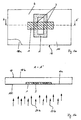
- FIG. 1a shows a carrier substrate 10 made of transparent PET, which has a prepared bottom 10 a.
- Figure 1 b shows the carrier substrate 10 from FIG. 1 a in section A - A '.
- the upper side of the carrier substrate 10 is designated by the reference numeral 10b.
- the underside 10a is provided in a first region 1 with a first diffractive relief structure and in a second region 2 with a second diffractive relief structure.
- the first and second relief structures are directly molded into the underside 10a of the carrier substrate, or the first and second relief structures are shaped into a replication lacquer layer provided on the underside.
- each of the first and second relief structures is a sine grid having a relief depth of 400 nm and a grating period of 350 nm, wherein the grating lines of the sine grating of the first relief structure are arranged substantially perpendicular to the grating lines of the sine grating of the second relief structure.
- Table 2 for such sine gratings a degree of transparency of 82.3% for the TE polarization direction and 62.8% for the TM polarization direction results.
- a relative difference in transparency of 30% results for the two different polarization directions.
- the azimuth angle of the first and second relief structure differs and the Depth-to-width ratio of the relief structure is preferably greater than 0.3.
- the relief structures exemplified in Table 2 with a grating period of 350 nm and a depth of 100 nm or 800 nm can be used, in which case the azimuth angle of the first and second relief structures preferably has an angular difference of approximately 90 °.
- a coating mask layer 100 of silver is sputtered over the entire surface in a constant area density with respect to the plane spanned by the carrier substrate 10.
- the first region 1 is so oriented for a according to the grid lines of the first relief structure, TE polarized light more transparent than the second region. Conversely, the second region is more transparent to the 90 ° polarized light than the first region.
- the third area in which a superposition of the first and second relief structure is provided (here cross-shaped sine grid with a depth of 400 nm and a grating period of 350 nm), the higher transmittance exists for both polarization directions.
- first exposure radiation 20a whose polarization direction is chosen so that the light is TE polarized with respect to the first relief structure
- second exposure radiation 20b which is an exposure to linearly polarized light having a wavelength of 550 nm and having a polarization direction rotated by 90 ° relative to the polarization direction of the exposure radiation 20a
- increased transmittance results in the second region 2 and third area 3.
- the exposure mask layer 100 is opaque and in a layer thickness, so that the fourth region 4 is impermeable to the first and the second exposure radiation 20a, 20b.
- Figure 1c shows the top 10b of the carrier substrate 10 from FIG. 1a upon exposure of the lower surface 10a to the first exposure radiation 20a.
- the exposure mask layer 100 has an increased permeability to the first exposure radiation 20a on the lower side 10a.
- Figure 1d shows the top 10b of the carrier substrate 10 from FIG. 1a upon exposure of the bottom 10a to the second exposure radiation 20b. Only in the second region 2 does the exposure mask layer 100 have an increased permeability for the second exposure radiation 20b on the underside 10a.
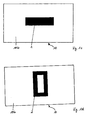
- FIG. 2a shows the carrier substrate 10 from FIG. 1a in section A - A 'with the first functional layer 30 of copper applied over its entire surface in a layer thickness of 0.1 .mu.m to 0.5 .mu.m and also a first negative photoresist layer 40 applied over the entire area.
- the first exposure radiation penetrates 20a amplifies in the first region 1 through the exposure mask layer 100, the carrier layer 10 and the first functional layer 30 and leads to a partially stronger exposure of the first photoresist layer 40.
- the exposure time and the exposure intensity are in this case matched to the photoresist used for the photoresist layer 40, that the photoresist is activated in the partially more exposed area 1, but is not activated in the less exposed areas 2 and 4.
- FIG. 2b shows the carrier substrate 10 from FIG. 2a after etching the first functional layer 30.
- the regions of the first functional layer 30 which were not covered by the etching mask were removed, so that a structured first functional layer 30 'was formed.
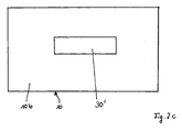
- Figure 2c shows the carrier substrate 10 from FIG. 2b after removal of the etching mask in plan view.
- the structured first functional layer 30 ' is present on the upper side 10a of the carrier substrate 10 in register with the first region 1 (see FIG. 1c) ,
- Figure 2d shows the carrier substrate 10 from Figure 2c in cross-section, with a third functional layer 50 of a transparent organic dielectric material applied over the entire area on the structured first functional layer 30 'and free areas of the carrier substrate 10.
- a second functional layer 31 made of copper in a layer thickness of 0.1 .mu.m to 0.5 .mu.m and a second positive photoresist layer 41 is also applied to the entire surface.
- the second exposure radiation 20b penetrates in the second region 2 through the exposure mask layer 100, the carrier layer 10, the first functional layer 30, the third functional layer 50 and the second functional layer 31, resulting in a partially stronger exposure of the second exposure beam 20b second photoresist layer 41.
- the exposure time and the exposure intensity are hereby adjusted to the photoresist used for the photoresist layer 41 such that the photoresist is in the partially more exposed area 2 is activated, but not activated in the less exposed areas 1 and 4.
- FIG. 2e shows the carrier substrate 10 from Figure 2d after development and structuring of the second photoresist layer or its remaining unexposed areas 41 ', and after etching of the second functional layer 31, wherein the structured second functional layer 31' was formed.
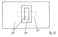
- FIG. 2f shows the carrier substrate 10 from FIG. 2e after removal of the structured second photoresist layer 41 'in plan view.
- the structured second functional layer 31 'on the third functional layer 50 can be seen.
- the position of the structured first functional layer 30 'below the third functional layer 50 is indicated by a dotted line.
- the structured first functional layer 30 ' is arranged in perfect register with the structured second functional layer 31'.
Description
Die Erfindung betrifft ein Verfahren zur Herstellung eines Mehrschichtkörpers, insbesondere eines Mehrschichtkörpers mit mindestens einem elektronischen Bauelement, wobei der Mehrschichtkörper mindestens zwei Funktionsschichten, insbesondere elektrische Funktionsschichten, auf einer Oberseite eines Trägersubstrats umfasst, welche im Register zueinander strukturiert sind. Die Erfindung betrifft weiterhin einen danach erhältlichen Mehrschichtkörper.The invention relates to a method for producing a multilayer body, in particular a multilayer body having at least one electronic component, wherein the multilayer body comprises at least two functional layers, in particular electrical functional layers, on an upper side of a carrier substrate, which are structured in register with one another. The invention further relates to a multi-layer body obtainable thereafter.
Dicke Trägersubstrate waren dabei bislang bevorzugt, da es sich bei der Verarbeitung dünner, kostengünstigerer Trägersubstrate mit einer Dicke im Bereich von 6 bis etwa 50 µm gezeigt hat, dass diese zu einem Verziehen während der Verarbeitung neigen, wobei der Verzug sich mit jedem Verarbeitungsschritt ändert. Wird auf das dünne Trägersubstrat eine elektrische Funktionsschicht aufgebracht und strukturiert, so ergibt sich bereits ein merklicher Verzug bzw. senkrecht zum Trägersubstrat gesehen eine Abweichung der Form der Funktionsschicht von deren Idealform. Der Verzug wirkt sich besonders störend aus, wenn nachfolgend oder nach Aufbringung einer oder mehrerer vollflächiger Funktionsschichten, verbunden mit einer weiteren Änderung der Dimensionen der bereits gebildeten strukturierten Funktionsschicht, eine weitere strukturierte Funktionsschicht zu der bereits gebildeten strukturierten Funktionsschicht im Register angeordnet werden muss.Thick support substrates have heretofore been preferred because processing of thinner, less costly support substrates having a thickness in the range of 6 to about 50 microns has been found to be prone to distortion during processing, with the distortion varying with each processing step. If an electrical functional layer is applied and patterned on the thin carrier substrate, a noticeable distortion or perpendicular to the carrier substrate already results in a deviation of the shape of the functional layer from its ideal shape. The delay has a particularly disturbing effect if, subsequently or after application of one or more full-surface functional layers, combined with a further change in the dimensions of the already formed structured functional layer, a further structured functional layer must be arranged in the register relative to the already formed structured functional layer.
Es ist daher Aufgabe der Erfindung, ein verbessertes Verfahren zur Herstellung eines Mehrschichtkörpers mit im Register zueinander strukturierten Funktionsschichten sowie danach herstellbare Bauelemente anzugeben, insbesondere ein verbessertes Verfahren zur Herstellung elektronischer Bauelemente auf zum Verziehen neigenden Trägersubstraten bereitzustellen.It is therefore an object of the invention to provide an improved method for producing a multilayer body with functional layers structured in register with one another and components which can be produced thereafter, in particular to provide an improved method for producing electronic components on carrier substrates which are prone to warping.
Die Aufgabe wird für das Verfahren zur Herstellung eines Mehrschichtkörpers, der mindestens zwei insbesondere elektrische Funktionsschichten auf einer Oberseite eines Trägersubstrats umfasst, welche im Register zueinander strukturiert sind, dadurch gelöst, dass eine Unterseite des Trägersubstrats derart präpariert wird, dass in einem ersten Bereich eine Durchlässigkeit für eine erste Belichtungsstrahlung und in mindestens einem zweiten Bereich eine Durchlässigkeit für mindestens eine dazu unterschiedliche zweite Belichtungsstrahlung im Register zum ersten Bereich resultiert, dass die Unterseite nacheinander mit der ersten und der mindestens einen zweiten Belichtungsstrahlung belichtet wird, und dass die erste Belichtungsstrahlung zur Strukturierung einer ersten Funktionsschicht und die mindestens eine zweite Belichtungsstrahlung zur Strukturierung mindestens einer zweiten Funktionsschicht auf der Oberseite des Trägersubstrats verwendet wird.The object is achieved for the method for producing a multilayer body, which comprises at least two, in particular electrically functional layers on an upper side of a carrier substrate, which are structured in register to each other, that a bottom of the carrier substrate is prepared such that in a first region, a permeability for a first exposure radiation and in at least one second region, a transmission for at least one different second exposure radiation in the register to the first region results in that the bottom is successively exposed to the first and the at least one second exposure radiation, and that the first exposure radiation for structuring a first functional layer and the at least one second exposure radiation is used for structuring at least one second functional layer on the upper side of the carrier substrate.
Das erfindungsgemässe Verfahren ermöglicht trotz eines Verzugs des Trägersubstrats bei dessen Verarbeitung eine unproblematische Anordnung der mindestens einen zweiten Funktionsschicht im perfekten oder nahezu perfekten Register zur ersten Funktionsschicht, da der auftretende Verzug gleichermassen den ersten Bereich und den mindestens einen zweiten Bereich betrifft. Die Form des ersten Bereichs wird senkrecht zur Ebene des Trägersubstrats gesehen im Einklang mit der Form des mindestens einen zweiten Bereichs durch den Verzug verändert, so dass sich die Lage des ersten Bereichs hinsichtlich der Lage des mindestens einen zweiten Bereichs nicht verschieben kann. Die Lage des ersten Bereichs sowie des mindestens einen zweiten Bereichs wird somit bereits zu Beginn des Herstellungsverfahrens auf dem Trägersubstrat festgelegt, so dass eine Ungenauigkeit in der Ausrichtung der ersten Funktionsschicht gegenüber der mindestens einen zweiten Funktionsschicht trotz eines Verzugs des Trägersubstrats nicht mehr auftreten kann. Die mindestens eine zweite Funktionsschicht wird in einer von ihrer Idealform abweichenden und in einer an die aktuell vorliegende Form der ersten Funktionsschicht angepassten Form lagegenau zur ersten Funktionsschicht ausgebildet. Aufgrund der genauen Positionierung der Funktionsschichten zueinander ist es nun möglich, hochwertige optische und/oder elektrische Bauelemente mit verbesserten optischen bzw. elektrischen Eigenschaften bei gleichzeitig geringerem Platzbedarf auf dem Trägersubstrat auszubilden.Despite the distortion of the carrier substrate during its processing, the method according to the invention makes possible an unproblematic arrangement of the at least one second functional layer in the perfect or nearly perfect register to the first functional layer, since the distortion occurring equally affects the first region and the at least one second region. The shape of the first region is changed perpendicular to the plane of the carrier substrate in accordance with the shape of the at least one second region by the distortion, so that the position of the first region with respect to the position of the at least one second region can not shift. The position of the first region and of the at least one second region is thus already established on the carrier substrate at the beginning of the production process, so that an inaccuracy in the orientation of the first functional layer relative to the at least one second functional layer can no longer occur despite a distortion of the carrier substrate. The at least one second functional layer is formed in a position that is different from its ideal shape and in a shape adapted to the currently present form of the first functional layer, in a positionally accurate manner relative to the first functional layer. Due to the precise positioning of the functional layers relative to one another, it is now possible to form high-quality optical and / or electrical components with improved optical or electrical properties while at the same time requiring less space on the carrier substrate.
So werden bei der Herstellung von OFETs auf einem dünnen Trägersubstrat aufgrund der optimalen Ausrichtung der Source/Drain-Elektroden gegenüber der Gate-Elektrode deutlich niedrigere Gate-Kapazitäten erreicht, so dass eine Schaltgeschwindigkeit der OFETs deutlich erhöht ist. Während bei den früheren Herstellungsmethoden ca. 80 % der Fläche des Trägersubstrats für die Berücksichtigung von Toleranzen bei der Herstellung der einzelnen Funktionsschichten verloren ging, ist nun eine deutlich bessere Ausnutzung der Fläche des Trägersubstrats möglich, so dass um bis zu 100 % mehr elektronische Bauelemente auf einem Trägersubstrat gebildet werden können.Thus, in the production of OFETs on a thin carrier substrate due to the optimal alignment of the source / drain electrodes relative to the gate electrode significantly lower gate capacitances are achieved, so that a switching speed of the OFETs is significantly increased. While approximately 80% of the surface of the carrier substrate was lost in the consideration of tolerances in the production of the individual functional layers in the earlier production methods, a significantly better utilization of the surface of the carrier substrate is now possible, meaning that up to 100% more electronic components are possible a carrier substrate can be formed.
Das erfindungsgemässe Verfahren bietet sich hier weiter vor allem zur Herstellung von optischen Bauelementen an, welche zwei strukturierte, von einer Abstandsschicht voneinander getrennte Funktionsschichten umfassen. Die beiden strukturierten Funktionsschichten können hierbei metallische oder farbige Schichten sein. Bevorzugt handelt es sich bei der ersten Funktionsschicht um eine opake Maskenschicht, welche bei Betrachtung eine winkelabhängige geometrische Abschattung der zweiten strukturierten Funktionsschicht bewirkt und so je nach Blickwinkel beispielsweise ein Farbflipp oder einen Wechsel der dargestellten Bildinformation erzeugt. Auch hier ist es möglich, dass die zwei oder mehr unabhängig voneinander strukturierbaren Funktionsschichten unmittelbar aufeinander liegen und so beispielsweise ein Farbbild durch additive oder substraktive Farbmischung bilden. Bei den Funktionsschichten kann es sich weiter auch um IR- oder UV-lumineszente unabhängig voneinander strukturierbare Schichten oder um Schichten handeln, die mit optisch variablen Pigmenten (Dünnfilmschicht-Pigmente, Flüssigkristall-Pigmente) versehen sind. Weiter ist es auch möglich, dass die optischen Funktionsschichten im weiteren auch von einem diffraktiven Oberflächen-Relief überlagert sind und so beispielsweise metallische oder dielektrische Reflexionsschichten darstellen, die die Generierung eines partiell vorhandenen optisch variablen Effekts (beispielsweise Hologramm) ermöglichen.The method according to the invention is furthermore particularly suitable for the production of optical components which comprise two structured functional layers separated from one another by a spacer layer. The two structured functional layers may be metallic or colored layers. The first functional layer is preferably an opaque mask layer which, when viewed, effects an angle-dependent geometrical shadowing of the second structured functional layer and thus generates, for example, a color flip or a change in the displayed image information depending on the viewing angle. Again, it is possible that the two or more independently structurable functional layers are directly adjacent to each other and thus form, for example, a color image by additive or subtractive color mixing. The functional layers may also be IR or UV-luminescent layers structurable independently of one another or layers which are provided with optically variable pigments (thin-film layer pigments, liquid crystal pigments). Furthermore, it is also possible for the optical functional layers to be superimposed on a diffractive surface relief and thus represent, for example, metallic or dielectric reflection layers which enable the generation of a partially present optically variable effect (for example a hologram).
Es kann vorgesehen sein, das Trägersubstrat auf der Unterseite direkt mit Reliefstrukturen zu versehen oder eine auf die Unterseite aufgebrachte Schicht, insbesondere aus einem thermoplastischen Material oder einem UV-Lack, mit Reliefstrukturen zu versehen. Dabei kann ein Spritzgusswerkzeug zum Einsatz kommen oder die Reliefstrukturen mittels Abformen eines Stempels in UV-Lack oder mittels eines gegebenenfalls beheizten Stempels in thermoplastischem Material gebildet werden. Auch die Verwendung einer klassischen Photolithographiemethode zur Bildung der Reliefstrukturen auf der Unterseite des Trägersubstrats, bei der ein Photoresist aufgetragen, belichtet, entwickelt und als Ätzmaske für die Unterseite verwendet wird, ist ohne weiteres möglich.It can be provided to provide the carrier substrate on the underside directly with relief structures or to provide a layer applied to the underside, in particular of a thermoplastic material or a UV coating, with relief structures. In this case, an injection molding tool can be used or the relief structures can be formed by molding a stamp in UV varnish or by means of an optionally heated stamp in thermoplastic material. Also, the use of a classical photolithography method to form the relief structures on the bottom Of the carrier substrate, in which a photoresist is applied, exposed, developed and used as an etching mask for the bottom, is readily possible.
Die Aufgabe wird für einen Mehrschichtkörper, insbesondere umfassend ein organisches elektronisches Bauelement, welcher ein Trägersubstrat aus einem flexiblen Folienmaterial, insbesondere einem Kunststofffolienmaterial, aufweist, dadurch gelöst, dass eine Unterseite des Trägersubstrats derart präpariert ist, dass in einem ersten Bereich eine Durchlässigkeit für eine erste Belichtungsstrahlung und in mindestens einem zweiten Bereich eine Durchlässigkeit für mindestens eine dazu unterschiedliche zweite Belichtungsstrahlung im Register zum ersten Bereich ausgebildet ist, und dass auf einer Oberseite des Trägersubstrats mindestens zwei strukturierte Funktionsschichten im Register zueinander und weiterhin im Register zu dem ersten und dem mindestens einen zweiten Bereich angeordnet sind.The object is achieved for a multilayer body, in particular comprising an organic electronic component, which has a carrier substrate made of a flexible film material, in particular a plastic film material, characterized in that an underside of the carrier substrate is prepared such that in a first region, a permeability to a first At least two structured functional layers in register with each other and further in the register to the first and the at least one second on a top side of the carrier substrate at least one second exposure radiation is formed in the register to the first region Area are arranged.
Das Trägersubstrat weist hierbei eine Dicke im Bereich von 3 µm bis 250 µm, bevorzugt 6 µm bis 50 µm auf.The carrier substrate in this case has a thickness in the range of 3 .mu.m to 250 .mu.m, preferably 6 .mu.m to 50 .mu.m.
Die erste und zweite Belichtungsstrahlung können sich hierbei beispielsweise durch ihre Wellenlänge, Polarisation, spektrale Zusammensetzung, den Beleuchtungseinfallwinkel, etc. unterscheiden.The first and second exposure radiation may differ, for example, by their wavelength, polarization, spectral composition, the angle of incidence of illumination, etc.
Das Bauelement weist aufgrund der genauen Positionierung der Funktionsschichten zueinander besonders gute und reproduzierbare optische und/oder elektrische Eigenschaften bei gleichzeitig geringem Platzbedarf auf.Due to the precise positioning of the functional layers relative to one another, the component has particularly good and reproducible optical and / or electrical properties while at the same time requiring little space.
In einer ersten Variante des erfindungsgemässen Verfahrens wird die Unterseite des Trägersubstrats präpariert, indem im ersten Bereich eine erste Reliefstruktur und im zweiten Bereich und im Register zur ersten Reliefstruktur mindestens eine, zur ersten Reliefstruktur unterschiedliche zweite Reliefstruktur gebildet wird, dass auf die Unterseite weiterhin eine Belichtungsmaskenschicht aufgebracht wird, wobei die Belichtungsmaskenschicht mit einer konstanten Flächendichte bezogen auf eine von der Trägerschicht aufgespannte Ebene aufgebracht wird, dass im Register zur ersten Reliefstruktur die auf die Oberseite des Trägersubstrat aufgebrachte erste Funktionsschicht strukturiert wird und dass im Register zu der mindestens einen zweiten Reliefstruktur die mindestens eine auf die Oberseite des Trägersubstrats aufgebrachte zweite elektrische Funktionsschicht strukturiert wird. Bei diesem Ausführungsbeispiel der Erfindung wird keine Belichtungsmaskenschicht benötigt.In a first variant of the inventive method, the underside of the carrier substrate is prepared by a first relief structure in the first region and in the second region and in register with the first relief structure at least one second relief structure different from the first relief structure is formed so that an exposure mask layer is applied to the underside, wherein the exposure mask layer is applied with a constant areal density relative to a plane spanned by the carrier layer, that in the register to the first relief structure that on top The first functional layer applied to the carrier substrate is structured, and the at least one second electrical functional layer applied to the upper side of the carrier substrate is patterned in register with the at least one second relief structure. In this embodiment of the invention, no exposure mask layer is needed.
Der ersten Variante des Verfahrens liegt die Erkenntnis zugrunde, dass durch die Reliefstrukturen im ersten und mindestens einen zweiten Bereich physikalische Eigenschaften der auf das Trägersubstrat aufgebrachten Belichtungsmaskenschicht, beispielsweise effektive Dicke oder optische Dichte, beeinflusst werden, so dass sich die Transmissions-Eigenschaften der Belichtungsmaskenschicht im ersten und zweiten Bereich unterscheiden. Die Belichtungsmaskenschicht wird in einem Belichtungsverfahren als Maske für die Teilentfernung der ersten elektrischen Funktionsschicht und weiterhin auch für die Teilentfernung der mindestens einen zweiten elektrischen Funktionsschicht verwendet, indem jeweils eine photoempfindliche Schicht auf der Oberseite des Trägersubstrats durch die Belichtungsmaskenschicht - also auch durch das Trägersubstrat - hindurch belichtet und partiell entfernt wird, so dass eine Strukturierung der ersten bzw. der zweiten Funktionsschicht unmittelbar erfolgt oder danach erfolgen kann.The first variant of the method is based on the finding that physical properties of the exposure mask layer applied to the carrier substrate, for example effective thickness or optical density, are influenced by the relief structures in the first and at least one second area, so that the transmission properties of the exposure mask layer in the first and second area differ. The exposure mask layer is used in an exposure method as a mask for the partial removal of the first electrical functional layer and also for the partial removal of the at least one second electrical functional layer, in each case by passing a photosensitive layer on the upper side of the carrier substrate through the exposure mask layer, ie also through the carrier substrate is exposed and partially removed, so that a structuring of the first and the second functional layer is carried out immediately or can be done afterwards.
Hierdurch wird gegenüber den mit herkömmlichen Verfahren aufgebrachten Funktionsschichten der Vorteil erzielt, dass diese ohne zusätzlichen Justieraufwand registergenau zueinander ausgerichtet sind. Es haben nur die Toleranzen der Reliefstrukturen Einfluss auf die Toleranzen der Lage der beiden Funktionsschichten. Die Anordnung von Bereichen der Belichtungsmaskenschicht mit gleichen physikalischen Eigenschaften erfolgt exakt im Register zum ersten und mindestens einen zweiten Bereich.As a result, compared to the functional layers applied with conventional methods, the advantage is achieved that they are aligned in register with each other without additional adjustment effort. Only the Tolerances of the relief structures Influence on the tolerances of the position of the two functional layers. The arrangement of areas of the exposure mask layer with the same physical properties takes place exactly in register with the first and at least one second area.
Das Trägersubstrat ist dabei möglichst dünn zu wählen, da der Abstand zwischen der strukturierten Schicht und der z.B. photoaktiven Schicht auf der gegenüberliegenden Seite, insbesondere bei dicken Trägern, einen Einfluss auf die Qualität/Auflösung/Register der Funktionsschicht haben kann.The carrier substrate should be as thin as possible, since the distance between the structured layer and the e.g. photoactive layer on the opposite side, especially with thick carriers, may have an impact on the quality / resolution / register of the functional layer.
Bei der Belichtungsmaskenschicht handelt es sich um eine Schicht, die eine Doppel-Funktion erfüllt, da sie die Funktion einer hochgenauen Belichtungsmaske für den Herstellungsprozess von unterschiedlich strukturierten Funktionsschichten erbringt.The exposure mask layer is a layer that performs a dual function because it provides the function of a high-precision exposure mask for the manufacturing process of differently structured functional layers.
Die Belichtungsmaskenschicht wird auf das Trägersubstrat vorzugsweise mittels Sputtern, Aufdampfen oder Aufsprühen aufgebracht. Beim Sputtern liegt prozessbedingt ein gerichteter Materialauftrag vor, so dass bei einem Aufsputtern von Material der Belichtungsmaskenschicht in konstanter Flächendichte bezogen auf die von dem Trägersubstrat aufgespannte Ebene das Material auf das mit den Reliefstrukturen versehene Trägersubstrat lokal unterschiedlich dick abgelagert wird. Beim Aufdampfen und Aufsprühen der Belichtungsmaskenschicht wird verfahrenstechnisch vorzugsweise ebenfalls ein zumindest teilweise gerichteter Materialauftrag erzeugt. Der Materialauftrag kann dabei nicht nur senkrecht, sondern auch in einem Winkel im Bereich von 30 bis 150° zur von dem Trägersubstrat aufgespannten Ebene erfolgen. Dies ist insbesondere bei der Verwendung periodischer symmetrischer oder asymmetrischer Reliefstrukturen von Vorteil, welche gezielt partiell beschichtet werden sollen.The exposure mask layer is preferably applied to the carrier substrate by means of sputtering, vapor deposition or spraying. When sputtering is due to the process, a directed material order, so that when sputtering material of the exposure mask layer in constant area density based on the plane spanned by the carrier substrate plane, the material is locally deposited differently thick on the provided with the relief structures carrier substrate. During vapor deposition and spraying of the exposure mask layer, an at least partially directed material application is preferably also produced by process engineering. The material application can be done not only vertically, but also at an angle in the range of 30 to 150 ° to the plane spanned by the carrier substrate level. This is particularly advantageous when using periodic symmetric or asymmetrical relief structures, which are selectively coated in a targeted manner should be.
Dabei wird die Belichtungsmaskenschicht vorzugsweise von einer Metallschicht oder von einer Schicht aus einer Metalllegierung gebildet. Solche Schichten können mit bewährten Verfahren, wie Sputtern, aufgebracht werden, und sie weisen bereits bei geringen Schichtdicken eine hinreichende optische Dichte auf. Es kann sich bei der Belichtungsmaskenschicht aber auch um eine nichtmetallische Schicht handeln, die beispielsweise eingefärbt sein kann, Flüssigkristalle enthalten kann oder dotiert sein kann, beispielsweise mit Nano-Partikeln oder mit Nano-Sphären, um ihre optische Dichte zu erhöhen.In this case, the exposure mask layer is preferably formed by a metal layer or by a layer of a metal alloy. Such layers can be applied by known methods, such as sputtering, and they have a sufficient optical density even at low layer thicknesses. However, the exposure mask layer can also be a nonmetallic layer, which can be colored, for example, can contain liquid crystals or can be doped, for example with nanoparticles or with nano spheres, in order to increase their optical density.
Weiter kann vorgesehen sein, dass die Belichtungsmaskenschicht auf das Trägersubstrat in einer Dicke aufgebracht wird, bei der die Belichtungsmaskenschicht weitgehend opak ist, vorzugsweise eine optische Dichte von grösser als 1,5 besitzt.It can further be provided that the exposure mask layer is applied to the carrier substrate in a thickness at which the exposure mask layer is substantially opaque, preferably has an optical density of greater than 1.5.
Überraschender Weise hat sich gezeigt, dass sich durch die Erhöhung der Opazität der Belichtungsmaskenschicht das Verhältnis der Transmissivitäten der Bereiche mit unterschiedlicher diffraktiver Reliefstruktur vergrössern lässt. Wird mit entsprechender Beleuchtungsstärke durch eine üblicherweise als opak bezeichnete Belichtungsmaskenschicht (beispielsweise optische Dichte von 5) belichtet, die aufgrund ihrer hohen optischen Dichte normalerweise nicht als Maskenschicht eingesetzt werden würde, lassen sich besonders gute Ergebnisse erzielen.Surprisingly, it has been shown that increasing the opacity of the exposure mask layer can increase the ratio of the transmissivities of the regions with different diffractive relief structure. If exposure is effected with an appropriate illuminance by an exposure mask layer (for example optical density of 5), which is normally designated as opaque, which would normally not be used as a mask layer because of its high optical density, particularly good results can be achieved.
Von besonderem Vorteil ist, wenn die Belichtungsmaskenschicht auf das Trägersubstrat vollflächig in einer Dicke aufgebracht wird, bei der die Belichtungsmaskenschicht eine optische Dichte zwischen 2 und 7 besitzt. Zur Ausbildung besonders grosser Unterschiede der optischen Dichte der ersten und der zweiten Reliefstruktur kann in dem ersten Bereich als erste Reliefstruktur eine diffraktive Reliefstruktur mit einem hohem Tiefen-zu-Breiten-Verhältnis der einzelnen Strukturelemente, insbesondere mit einem Tiefen-zu-Breiten-Verhältnis > 0,3, abgeformt werden und die zweite Reliefstruktur als Reliefstruktur mit niedrigerem Tiefen-zu-Breiten-Verhältnis ausgebildet werden.It is particularly advantageous if the exposure mask layer is applied to the carrier substrate over its entire surface in a thickness at which the exposure mask layer has an optical density between 2 and 7. For the formation of particularly large differences in the optical density of the first and the second relief structure may be in the first region as a first relief structure, a diffractive relief structure with a high depth-to-width ratio of the individual structural elements, in particular with a depth-to-width ratio> 0.3, molded and the second relief structure be formed as a relief structure with lower depth-to-width ratio.
Durch die Verwendung derartiger spezieller diffraktiver Reliefstrukturen ist es bei geeigneter Wahl der Schichtdicke der Belichtungsmaskenschicht möglich, sehr grosse, bereits mit dem Auge erkennbare Unterschiede in der optischen Dichte der ersten Schicht im ersten Bereich und im zweiten Bereich zu generieren. Überraschenderweise wurde jedoch festgestellt, dass derart grosse Unterschiede in der Transmission im ersten und im zweiten Bereich für die Umsetzung des erfindungsgemässen Verfahrens nicht zwingend sind. Es kommt nur darauf an, dass sich der erste und der mindestens eine zweite Bereich durch ihre Transmissionseigenschaften beziehungsweise eine geringere oder eine grössere optische Dichte abgrenzen.By using such special diffractive relief structures, it is possible, with a suitable choice of the layer thickness of the exposure mask layer, to generate very large differences in the optical density of the first layer in the first region and in the second region which are already recognizable with the eye. Surprisingly, however, it was found that such large differences in the transmission in the first and in the second range for the implementation of the inventive method are not mandatory. It is only important that the first and the at least one second region delimit by their transmission properties or a lower or a greater optical density.
In einer vorteilhaften Ausgestaltung ist vorgesehen, dass die photoempfindliche Schicht durch die Belichtungsmaskenschicht hindurch mittels UV-Strahlung belichtet wird. Experimente haben gezeigt, dass die durch die unterschiedliche Gestaltung der Reliefstruktur im ersten und zweiten Bereich erzielbaren Unterschiede in den Transmissionseigenschaften der Belichtungsmaskenschicht im Bereich der UV-Strahlung besonders ausgeprägt sind. Bei der Verwendung von UV-Strahlung für die Belichtung lassen sich so besonders gute Ergebnisse erzielen.In an advantageous embodiment, it is provided that the photosensitive layer is exposed through the exposure mask layer by means of UV radiation. Experiments have shown that the differences in the transmission properties of the exposure mask layer in the region of the UV radiation which can be achieved by the different design of the relief structure in the first and second regions are particularly pronounced. When using UV radiation for the exposure, particularly good results can be achieved.
Reliefstrukturen mit geringen Unterschieden im Tiefen-zu-Breiten-Verhältnis weisen bei dünner Bedampfung auch üblicherweise relativ geringe Unterschiede in der Transmission auf. Selbst geringe relative Unterschiede können jedoch verstärkt werden durch Vergrösserung der Schichtdicke der Belichtungsmaskenschicht und damit der mittleren optischen Dichte. So lassen sich bereits bei recht geringen Unterschieden der Transmission der Belichtungsmaskenschicht im ersten und im zweiten Bereich gute Ergebnisse erzielen. Bei der Belichtungsmaskenschicht kann es sich um eine sehr dünne Schicht in der Grössenordnung von einigen nm handeln. Die mit gleichmässiger Flächendichte bezogen auf die von dem Trägersubstrat aufgespannte Ebene aufgetragene Belichtungsmaskenschicht ist in Bereichen mit einem hohen Tiefen-zu-Breiten-Verhältnis erheblich dünner ausgebildet als in Bereichen mit niedrigerem Tiefen-zu-Breiten-Verhältnis.Relief structures with small differences in the depth-to-width ratio also usually show relatively small differences in transmission with thin vapor deposition. Even small relative differences However, they can be enhanced by increasing the layer thickness of the exposure mask layer and thus the average optical density. Thus, even with quite small differences in the transmission of the exposure mask layer in the first and in the second range, good results can be achieved. The exposure mask layer may be a very thin layer, on the order of a few nm. The exposure mask layer applied with uniform areal density relative to the plane defined by the carrier substrate is made substantially thinner in areas having a high depth-to-width ratio than in areas having a lower depth-to-width ratio.
Das dimensionslose Tiefen-zu-Breiten-Verhältnis h/d ist ein kennzeichnendes Merkmal für die Vergrösserung der Oberfläche bei Verwendung von vorzugsweise periodischen Strukturen, beispielsweise mit sinusquadratischem Verlauf. Als Tiefe ist hier der Abstand zwischen dem höchsten und dem tiefsten aufeinander folgenden Punkt einer solchen Struktur bezeichnet, d.h. es handelt sich um den Abstand zwischen "Berg" und "Tal". Als Breite ist der Abstand zwischen zwei benachbarten höchsten Punkten, d.h. zwischen zwei "Bergen", bezeichnet. Je höher nun das Tiefen-zu-Breiten-Verhältnis ist, desto steiler sind die "Bergflanken" ausgebildet und desto dünner ist die auf den "Bergflanken" abgeschiedene erste Schicht ausgebildet. Der Effekt der Ausbildung höherer Transmission oder Transparenz bei Zunahme des Tiefen-zu-Breiten-Verhältnisses wird auch bei Strukturen mit vertikalen Flanken beobachtet, beispielsweise bei Rechteckgittern. Es kann sich aber auch um Strukturen handeln, auf die dieses Modell nicht anwendbar ist. Beispielsweise kann es sich um diskret verteilte linienförmige Bereiche handeln, die nur als ein "Tal" ausgebildet sind, wobei der Abstand zwischen zwei "Tälern" um ein Vielfaches höher ist als die Tiefe der "Täler". Bei formaler Anwendung der vorstehend genannten Definition würde das so berechnete Tiefen-zu-Breiten-Verhältnis annähernd Null sein und nicht das charakteristische physikalische Verhalten widerspiegeln. Deshalb ist bei diskret angeordneten Strukturen, die im wesentlichen nur aus einem "Tal" gebildet sind, die Tiefe des "Tales" zur Breite des "Tales" ins Verhältnis zu setzen.The dimensionless depth-to-width ratio h / d is a characteristic feature for the enlargement of the surface when using preferably periodic structures, for example with a sinusoidal course. Depth is the distance between the highest and the lowest consecutive point of such a structure, ie the distance between "mountain" and "valley". Width is the distance between two adjacent highest points, ie between two "mountains". The higher the depth-to-width ratio, the steeper the "mountain flanks" and the thinner the first layer deposited on the "mountain flanks". The effect of forming higher transmission or transparency as the depth-to-width ratio increases is also observed in structures having vertical edges, such as rectangular gratings. But they can also be structures to which this model is not applicable. For example, they may be discretely distributed line-shaped areas which are formed only as a "valley", wherein the distance between two "valleys" is many times higher than the depth of the "valleys". In formal application of the above definition, the thus calculated depth-to-width ratio would be close to zero and do not reflect the characteristic physical behavior. Therefore, with discretely arranged structures formed essentially only of a "valley", the depth of the "valley" should be related to the width of the "valley".
Der Grad der Verringerung der optischen Dichte kann in Abhängigkeit vom Untergrund, von der Beleuchtung usw. variieren. Eine wichtige Rolle spielt dabei die Absorption des Lichtes in der Belichtungsmaskenschicht.The degree of optical density reduction may vary depending on the background, lighting, etc. An important role is played by the absorption of light in the exposure mask layer.
Tabelle 1 zeigt den ermittelten Reflexionsgrad von zwischen Plastikfolien (Brechungsindex n = 1,5) angeordneten Belichtungsmaskenschichten aus Metall, insbesondere aus Ag, Al, Au, Cr, Cu, Rh und Ti bei einer LichtWellenlänge λ = 550 nm. Das Dickenverhältnis ε ist hierbei als Quotient aus der für den Reflexionsgrad R = 80% des Maximums Rmax und der für den Reflexionsgrad R = 20% des Maximums Rmax erforderlichen Dicke t der Metallschicht gebildet.
Aus der heuristischen Betrachtung heraus haben Silber und Gold (Ag und Au), wie zu sehen ist, einen hohen maximalen Reflexionsgrad RMax und erfordern ein relativ kleines Tiefen-zu-Breiten-Verhältnis zur Reduzierung der optischen Dichte der metallischen Belichtungsmaskenschicht, in dem vorstehenden Beispiel zur Ausbildung von Transparenz. Aluminium (Al) hat zwar ein auch einen hohen maximalen Reflexionsgrad RMax, erfordert aber ein höheres Tiefen-zu-Breiten-Verhältnis. Vorzugsweise kann deshalb vorgesehen sein, die Belichtungsmaskensschicht aus Silber oder Gold auszubilden.From the heuristic point of view, as can be seen, silver and gold (Ag and Au) have a high maximum reflectance R Max and require a relatively small depth to width ratio to reduce the optical density of the metallic exposure mask layer in the above Example of training for transparency. Although aluminum (Al) also has a high maximum reflectance R Max , it requires a higher depth-to-width ratio. Preferably, therefore, it may be provided to form the exposure mask layer of silver or gold.
Tabelle 2 zeigt nun die Berechnungsergebnisse, gewonnen aus strengen Beugungsberechnungen für als lineare, sinusförmige Gitter mit einem Gitterabstand von 350 nm ausgebildete Reliefstrukturen mit unterschiedlichen Tiefen-zu-Breiten-Verhältnissen. Die Reliefstrukturen sind mit Silber beschichtet mit einer nominalen Dicke t0 = 40 nm. Das Licht, das auf die Reliefstrukturen auftrifft, hat die Wellenlänge λ = 550 nm (grün) und ist TE-polarisiert bzw. TMpolarisiert.
Wie sich zeigte, ist die Transmission ausser vom Tiefen-zu-Breiten-Verhältnis auch abhängig von der Polarisation des aufgestrahlten Lichtes. Diese Abhängigkeit ist in Tabelle 2 für das Tiefen-zu-Breiten-Verhältnis h/d = 1,1 dargestellt. Es kann vorgesehen sein, diesen Effekt für die selektive Ausbildung von Funktionsschichten zu nutzen.As it turned out, apart from the depth-to-width ratio, the transmission is also dependent on the polarization of the radiated light. This dependence is shown in Table 2 for the depth to width ratio h / d = 1.1. It may be provided to use this effect for the selective formation of functional layers.
Weiterhin zeigte sich, dass der Transparenzgrad bzw. der Reflexionsgrad der Belichtungsmasken wellenlängenabhängig ist. Dieser Effekt ist besonders gut für TE-polarisiertes Licht ausgeprägt.Furthermore, it was found that the degree of transparency or the reflectance of the exposure masks is wavelength-dependent. This effect is especially good for TE polarized light.
Weiterhin zeigte sich, dass der Transparenzgrad bzw. die Transmission abnimmt, wenn der Einfallswinkel des Lichtes sich vom normalen Einfallswinkel unterscheidet, d.h. der Transparenzgrad nimmt ab, wenn das Licht nicht senkrecht einfällt. Das bedeutet, dass die Belichtungsmaskenschicht nur in einem begrenzten Einfallskegel des Lichtes transparent bzw. transparenter ausgebildet sein kann. Es kann also vorgesehen sein, dass die Belichtungsmaskenschicht bei schräger Beleuchtung opak oder undurchlässig ausgebildet ist, wobei auch dieser Effekt für die selektive Ausbildung weiterer Funktionsschichten nutzbar ist.Furthermore, it has been found that the degree of transparency or transmission decreases when the angle of incidence of the light differs from the normal angle of incidence, i. the degree of transparency decreases when the light is not incident vertically. This means that the exposure mask layer can be made transparent or transparent only in a limited incidence cone of the light. It can thus be provided that the exposure mask layer is formed opaque or impermeable in oblique illumination, whereby this effect can be used for the selective formation of further functional layers.
Neben dem Tiefen-zu-Breiten-Verhältnis einer Reliefstruktur wird die Veränderung der optischen Dichte auch durch die Spatialfrequenz der Reliefstruktur beeinflusst. So hat sich weiter gezeigt, dass eine Veränderung des Transmissionsverhaltens einer auf eine Reliefstruktur aufgebrachten Belichtungsmaskenschicht erzielt werden kann, wenn das Produkt aus Spatialfrequenz und Relieftiefe in einem ersten Bereich der Reliefstruktur grösser als das Produkt aus Spatialfrequenz und Relieftiefe in einem zweiten Bereich der Reliefstruktur ist.In addition to the depth-to-width ratio of a relief structure, the change in the optical density is also influenced by the spatial frequency of the relief structure. It has thus been further shown that a change in the transmission behavior of an exposure mask layer applied to a relief structure can be achieved if the product of spatial frequency and relief depth in a first region of the relief structure is greater than the product of spatial frequency and relief depth in a second region of the relief structure.
Die Ausbildung von Bereichen unterschiedlicher Transparenz bzw. Transmission kann aber auch durch andere Effekte erreicht werden, beispielsweise durch
- die Polarisationsabhängigkeit der Transmission infolge unterschiedlich orientierter Strukturen;
- den Formfaktor der Strukturen, d.h. Strukturen mit rechteckförmigem, sinusförmigem, sägezahnförmigem oder sonstigem Profil können bei gleichem Produkt aus Spatialfrequenz und Relieftiefe eine unterschiedliche Transmission aufweisen;
- gerichtetes Aufdampfen der Belichtungsmaskenschicht in Kombination mit speziellen Strukturen bzw. Strukturkombinationen oder Strukturanordnungen.
- the polarization dependence of the transmission due to differently oriented structures;
- the form factor of the structures, ie structures with rectangular, sinusoidal, sawtooth or other profile can have a different transmission with the same product of Spatialfrequenz and relief depth;
- directed vapor deposition of the exposure mask layer in combination with special structures or structural combinations or structural arrangements.
Wenn es sich bei der ersten Reliefstruktur um eine Struktur mit einem stochastischen Profil handelt, beispielsweise um eine Mattstruktur, können Korrelationslänge, Rauhtiefe und statistische Verteilung des Profils typische Kenngrössen sein, welche die Transmission beeinflussen.If the first relief structure is a structure with a stochastic profile, for example a matt structure, the correlation length, roughness depth and statistical distribution of the profile can be typical parameters which influence the transmission.
Zur Ausbildung von Bereichen mit unterschiedlicher Transparenz oder Transmission ist es so auch möglich, im ersten Bereich und im zweiten Bereich Reliefstrukturen zu verwenden, die sich in ein oder mehreren der oben aufgeführten Parameter unterscheiden.In order to form regions with different transparency or transmission, it is thus also possible to use relief structures in the first region and in the second region which differ in one or more of the parameters listed above.
In einer zweiten Variante des erfindungsgemässen Verfahrens wird die Unterseite des Trägersubstrats präpariert, indem in dem ersten Bereich eine erste Reliefstruktur und in dem zweiten Bereich und im Register zur ersten Reliefstruktur mindestens eine, zur ersten Reliefstruktur unterschiedliche zweite Reliefstrukturen gebildet wird, dass im Register zur ersten Reliefstruktur die auf die Oberseite des Trägersubstrat aufgebrachte erste Funktionsschicht strukturiert wird und dass im Register zu der mindestens einen zweiten Reliefstruktur die mindestens eine auf die Oberseite des Trägersubstrats aufgebrachte zweite Funktionsschicht strukturiert wird.In a second variant of the method according to the invention, the underside of the carrier substrate is prepared by forming a first relief structure in the first region and at least one second relief structure different from the first relief structure in the second region and in register with the first relief structure Relief structure is structured on the top of the carrier substrate applied first functional layer and that in the register to the at least one second Relief structure, the at least one applied to the top of the carrier substrate second functional layer is structured.
Die unterschiedlichen Belichtungseigenschaften ergeben sich hier aufgrund der unterschiedlichen Beugung, Brechung oder Reflexion der Belichtungsstrahlung an den gebildeten Reliefstrukturen.The different exposure properties arise here due to the different diffraction, refraction or reflection of the exposure radiation to the relief structures formed.
Die erste und zweite Belichtungsstrahlung unterscheidet sich bei diesem Ausführungsbeispiel bevorzugt in ihrem Einfallswinkel und/oder in ihrer Wellenlänge. So ist es beispielsweise möglich, als erste und zweite Reliefstrukturen Linsenstrukturen, beispielsweise Zylinder-Linsen oder Freiform-Linsen, vorzusehen, die bei unterschiedlichem Einfall der Belichtungsstrahlung das einfallende Licht im ersten Bereich oder im zweiten Bereich fokusieren und so die Durchlässigkeit des Trägersubstrats im ersten und zweiten Bereich abhängig von der Belichtungsrichtung erhöhen. Weiter ist es möglich, diffraktive Reliefstrukturen auf der Unterseite des Trägersubstrats vorzusehen, welche das Licht in Abhängigkeit von Einfallswinkel und/oder von der Wellenlänge durch Beugung in unterschiedlichen Bereichen fokusieren. So ist es zum einen möglich, diffraktive Linsen vorzusehen, die abhängig von der Wellenlänge des einfallenden Lichts einen unterschiedlichen Fokus besitzen und so das Licht bei einer ersten Belichtungsstrahlung im ersten Bereich und bei einer zweiten Belichtungsstrahlung, die sich von der ersten Belichtungsstrahlung in ihrer Wellenlänge unterscheidet, im zweiten Bereich fokusieren. Weiter ist es möglich, Blazegitter zu verwenden, die sich durch ein sägezahnförmiges Reliefprofil auszeichnen. Hierbei ist es möglich, den Einfallswinkel bezüglich der Flanken des Sägezahns so zu wählen, dass bei einem ersten Einfallswinkels des Lichts eine Totalreflexion (bei Aufbringen einer speziellen LRI-Schicht (auf die Blazestruktur) - (LRI = Low Refractive Index) - an der Flanke des Sägezahns stattfindet und bei einem zweiten Einfallswinkel des Lichts die Lichtstrahlen auf den durch den Brechungswinkel bestimmten Bereich gelenkt werden. Weiter ist es möglich, durch geeignete Wahl der Blazeparameter (Tiefe, Periode, Material, etc.) zu erreichen, dass zumindest ein signifikanter Unterschied in der transmittierten Intensität für die beiden Einfallswinkel existiert.The first and second exposure radiation preferably differs in this embodiment in their angle of incidence and / or in their wavelength. Thus, it is possible, for example, to provide lens structures, for example cylindrical lenses or free-form lenses, as the first and second relief structures, which focus the incident light in the first region or in the second region with different incidence of the exposure radiation and thus the permeability of the carrier substrate in the first and second relief structures increase the second range depending on the exposure direction. Furthermore, it is possible to provide diffractive relief structures on the underside of the carrier substrate, which focus the light as a function of angle of incidence and / or of the wavelength by diffraction in different regions. Thus, it is firstly possible to provide diffractive lenses which have a different focus depending on the wavelength of the incident light and thus the light at a first exposure radiation in the first region and at a second exposure radiation which differs from the first exposure radiation in its wavelength to focus in the second area. Furthermore, it is possible to use blaze gratings, which are characterized by a sawtooth-shaped relief profile. In this case, it is possible to choose the angle of incidence with respect to the edges of the sawtooth such that at a first angle of incidence of the light a total reflection (when applying a special LRI layer (on the bladder structure) - (LRI = Low Refractive Index) - on the flank of the sawtooth takes place and at a second angle of incidence of the light Beams are directed to the determined by the refractive angle range. Furthermore, it is possible to achieve, by a suitable choice of the blaze parameters (depth, period, material, etc.), that at least a significant difference in the transmitted intensity exists for the two angles of incidence.
Weiter ist es auch möglich, dass die ersten und zweiten Reliefstrukturen mit einer optischen Trennschicht, beispielsweise einer HRI-Schicht (z.B. ZnS) versehen werden.Furthermore, it is also possible for the first and second relief structures to be provided with an optical separation layer, for example an HRI layer (for example ZnS).
Mittels der ersten und zweiten Variante des Verfahren lassen sich strukturierte Funktionsschichten sehr hoher Auflösung erzielen. Die erzielbare Registrierung und Auflösung ist etwa um den Faktor 100 besser als durch bekannte Strukturierungsverfahren erzielbar. Da die Breite der Strukturelemente der ersten Reliefstruktur im Bereich der Wellenlänge des sichtbaren Lichtes (circa 380 bis 780 nm), aber auch darunter liegen kann, können Funktionsschichtbereiche mit sehr feinen Konturen ausgebildet werden. Damit werden auch in dieser Hinsicht grosse Vorteile gegenüber den bisher verwendeten Verfahren erzielt, da eine weitere Miniaturisierung des Bauelements erfolgen kann.By means of the first and second variant of the method, structured functional layers of very high resolution can be achieved. The achievable registration and resolution is about 100 times better than achievable by known structuring method. Since the width of the structural elements of the first relief structure can be in the range of the wavelength of the visible light (approximately 380 to 780 nm), but also below it, functional layer areas can be formed with very fine contours. Thus, great advantages over the previously used methods are achieved in this regard, as a further miniaturization of the device can be done.
Es können Linien und/oder Punkte mit hoher Auflösung erzeugt werden, beispielsweise mit einer Breite bzw. einem Durchmesser von weniger als 5 µm, insbesondere bis etwa 200 nm. Vorzugsweise werden Auflösungen im Bereich von etwa 0,5 µm bis 5 µm, insbesondere im Bereich von etwa 1 µm, erzeugt. Demgegenüber sind mit Verfahren, die eine Justierung der strukturierten Funktionsschichten im Register vorsehen, Linienbreiten kleiner als 10 µm nur mit sehr hohem Aufwand realisierbar.It is possible to produce lines and / or dots with high resolution, for example with a width or a diameter of less than 5 μm, in particular up to approximately 200 nm. Preferably, resolutions in the range from approximately 0.5 μm to 5 μm, in particular in the Range of about 1 micron, generated. In contrast, with methods that provide an adjustment of the structured functional layers in the register, line widths smaller than 10 microns can be realized only with great effort.
Es ist bevorzugt, wenn die erste und/oder die mindestens eine zweite Reliefstruktur als diffraktive Reliefstrukturen ausgebildet werden. Dabei hat es sich bewährt, wenn sich die erste und die mindestens eine zweite Reliefstruktur in ihrem Azimut unterscheiden.It is preferred if the first and / or the at least one second relief structure are formed as diffractive relief structures. It has proven useful if the first and the at least one second relief structure differ in their azimuth.
Die erste und/oder die mindestens eine zweite Reliefstruktur werden insbesondere als Gitterstruktur, wie Lineargitter oder Kreuzgitter, als isotrope oder anisotrope Mattstruktur, als binäre oder kontinuierliche Fresnellinse, als Mikroprisma, als Blazegitter, als Kombinationsstruktur oder als Makrostruktur ausgebildet:
- Lineargitter: z.B. Sinusgitter mit Linienzahlen von 100 l/mm bis 5000 l/mm
und Strukturtiefen von 50 nm bis 5 um. - Kreuzgitter: z.B. Sinusgitter mit Linienzahlen von 100 l/mm bis 5000 l/mm
und Strukturtiefen von 50 nm bis 5 µm. - Mattstrukturen (isotrop/anisotrop): Korrelationslängen von 0,5 µm bisss 50µm
und Strukturtiefen von 50nm bis 10 µm. - Blazegitter oder Mikroprismen: Linienzahlen von 10 l/mm bis 3000 l/mm und Strukturtiefen von 25 nm bis 10µm.
- Makrostruktur: beliebig geformte Oberflächenstrukturen, charakterisiert durch maximale
Tiefe von 100 nm bis 10µm, mit grossen Entfernungen (≥ 100 µm) zwischen Unsteigkeitsstellen des Oberflächenprofils. - Kombinatonsstrukturen: ergeben sich aus Kombinationen oben genannter Strukturen.
- Linear grids: eg sine grids with line numbers from 100 l / mm to 5000 l / mm and structure depths from 50 nm to 5 μm.
- Cross gratings: eg sine gratings with line numbers from 100 l / mm to 5000 l / mm and structure depths from 50 nm to 5 μm.
- Matt structures (isotropic / anisotropic): Correlation lengths of 0.5 μm to 50 μm and structure depths of 50 nm to 10 μm.
- Blaze grates or microprisms: Line numbers from 10 l / mm to 3000 l / mm and structure depths from 25 nm to 10μm.
- Macrostructure: arbitrarily shaped surface structures, characterized by a maximum depth of 100 nm to 10 μm, with large distances (≥ 100 μm) between points of elevation of the surface profile.
- Combination structures: result from combinations of the above-mentioned structures.
Gemäss einer dritten Variante des erfindungsgemässen Verfahrens wird die Unterseite des Trägersubstrats präpariert, indem in dem ersten Bereich eine erste Farbschicht und in dem zweiten Bereich und im Register zur ersten Farbschicht mindestens eine, zur ersten Farbschicht farblich unterschiedliche zweite Farbschicht angeordnet wird, und dass im Register zur ersten Farbschicht die auf die Oberseite des Trägersubstrat aufgebrachte erste Funktionsschicht strukturiert wird und dass im Register zu der mindestens einen zweiten Farbschicht die mindestens eine auf die Oberseite des Trägersubstrats aufgebrachte zweite elektrische Funktionsschicht strukturiert wird. Die unterschiedlichen Farbschichten wirken dabei als Filter für Belichtungsstrahlungen unterschiedlicher Wellenlängen.According to a third variant of the method according to the invention, the underside of the carrier substrate is prepared by arranging a first color layer in the first region and at least one second color layer different in color from the first color layer in the second region and in register with the first color layer, and in the register for the first color layer, the first functional layer applied to the upper side of the carrier substrate is structured, and in the register to the at least one second color layer the at least one second electrical functional layer applied to the upper side of the carrier substrate is structured. The different color layers act as filters for exposure radiation of different wavelengths.
Dabei wird beispielsweise im ersten Bereich musterförmig eine rote Farbschicht aufgedruckt, welche für eine blaue erste Belichtungsstrahlung durchlässig ist, und in einem zweiten Bereich eine blaue Farbschicht aufgedruckt, welche für eine rote zweite Belichtungsstrahlung durchlässig ist. Von der ersten und zweiten Farbschicht freie Bereiche des Trägersubstrats lassen beide Belichtungsstrahlungen durch, während Bereiche, welche mit beiden Farbschichten bedeckt sind, keine der beiden Belichtungsstrahlungen durchlassen.In this case, for example, a red color layer is pattern-shaped in the first area, which is permeable to a blue first exposure radiation, and printed in a second area, a blue color layer which is transparent to a red second exposure radiation. Both of the first and second color layer free areas of the carrier substrate let both exposure radiation through, while areas which are covered with two color layers, neither of the two exposure radiation pass.
Gemäss der ersten, zweiten oder dritten Variante wird auf die Oberseite des Trägersubstrats bevorzugt die erste Funktionsschicht vollflächig aufgebracht wird, wobei vor oder nach Bildung der ersten Funktionsschicht auf der Oberseite vollflächig eine erste photoempfindliche Schicht gebildet wird. Danach erfolgt eine Belichtung der ersten photoempfindlichen Schicht mittels der ersten Belichtungsstrahlung durch das Trägersubstrat und gegebenenfalls die Belichtungsmaskenschicht hindurch, welche im ersten Bereich für die erste Belichtungsstrahlung durchlässig ist/sind, und die erste photoempfindliche Schicht wird im Register zum ersten Bereich partiell entfernt, wobei unmittelbar oder nachfolgend eine Strukturierung der ersten Funktionsschicht erfolgt. Weiterhin wird die mindestens eine zweite Funktionsschicht vollflächig auf die Oberseite aufgebracht, wobei vor oder nach Bildung der mindestens einen zweiten Funktionsschicht vollflächig mindestens eine zweite photoempfindliche Schicht auf der Oberseite gebildet wird. Nun erfolgt eine Belichtung der mindestens einen zweiten photoempfindlichen Schicht mittels mindestens der zweiten Belichtungsstrahlung durch das Trägersubstrat und gegebenenfalls die Belichtungsmaskenschicht hindurch, welche(s) im zweiten Bereich für die zweite Belichtungsstrahlung durchlässig ist/sind, und die mindestens eine zweite photoempfindliche Schicht wird im Register zum zweiten Bereich partiell entfernt, wobei unmittelbar oder nachfolgend eine Strukturierung der mindestens einen zweiten Funktionsschicht erfolgt.According to the first, second or third variant, the first functional layer is preferably applied over the full area to the upper side of the carrier substrate, wherein a first photosensitive layer is formed over the whole area before or after formation of the first functional layer on the upper side. Thereafter, the first photosensitive layer is exposed by the first exposure radiation through the carrier substrate and optionally the exposure mask layer, which is permeable to the first exposure radiation in the first region, and the first photosensitive layer Layer is partially removed in the register to the first area, wherein structuring of the first functional layer takes place directly or subsequently. Furthermore, the at least one second functional layer is applied over its entire surface to the upper side, wherein at least one second photosensitive layer is formed over its entire surface before or after formation of the at least one second functional layer. Now, the at least one second photosensitive layer is exposed by at least the second exposure radiation through the carrier substrate and optionally the exposure mask layer, which is permeable to the second exposure radiation in the second region, and the at least one second photosensitive layer is registered Partially removed to the second region, wherein structuring of the at least one second functional layer takes place directly or subsequently.
Es hat sich bewährt, wenn die Unterseite des Trägersubstrats in einem dritten Bereich derart präpariert wird, dass der dritte Bereich sowohl für die erste als auch für die mindestens eine zweite Belichtungsstrahlung durchlässig ist. Dadurch lassen sich Bereiche der strukturierten ersten und der mindestens einen strukturierten zweiten Funktionsschicht deckungsgleich übereinander anordnen. Im Falle der ersten und zweiten Variante mit Reliefstrukturen werden die unterschiedlichen Reliefstrukturen im dritten Bereich nebeneinander oder sich überlagernd ausgebildet. Im. Fall der dritten Variante werden im dritten Bereich keine Farbschichten angeordnet.It has proven useful if the underside of the carrier substrate is prepared in a third region such that the third region is permeable to both the first and the at least one second exposure radiation. As a result, regions of the structured first and the at least one structured second functional layer can be arranged congruently one above the other. In the case of the first and second variant with relief structures, the different relief structures in the third area are formed next to each other or superimposed. In the case of the third variant, no color layers are arranged in the third area.
Weiterhin hat es sich bewährt, wenn die Unterseite des Trägersubstrats in einem vierten Bereich derart präpariert wird, dass der vierte Bereich undurchlässig für die erste und mindestens eine zweite Belichtungsstrahlung ist. Im Falle der ersten und zweiten Variante mit Reliefstrukturen werden keine oder ausgewählte Reliefstrukturen im dritten Bereich ausgebildet. Im Fall der dritten Variante werden im dritten Bereich alle Farbschichten angeordnet.Furthermore, it has proven useful if the underside of the carrier substrate is prepared in a fourth region such that the fourth region is impermeable to the first and at least one second exposure radiation. In the case of the first and second variant with relief structures are no or selected relief structures formed in the third region. In the case of the third variant, all color layers are arranged in the third area.
Somit lassen sich mindestens vier unterschiedliche Belichtungszustände realisieren:
- a) Belichten nur im ersten Bereich;
- b) Belichten nur im mindestens einen zweiten Bereich;
- c) Belichten im ersten und im mindestens einen zweiten Bereich;
- d) nicht Belichten;
- a) exposure only in the first area;
- b) exposing only in at least a second area;
- c) exposing in the first and at least a second area;
- d) not exposing;
Es hat sich bewährt, wenn das unpräparierte Trägersubstrat aus einem Material und/oder in einer Dicke ausgebildet wird, so dass es für die erste und/oder die mindestens eine zweite Belichtungsstrahlung durchlässig ist. Das unpräparierte Trägersubstrat kann aber auch so ausgebildet werden, dass es für die erste und/oder die mindestens eine zweite Belichtungsstrahlung undurchlässig ist und erst durch die Präparation, beispielsweise durch das Einbringen von Reliefstrukturen, oder beim Belichten, beispielsweise durch chemische Reaktionen usw., zumindest partiell für die Belichtungsstrahlung durchlässig wird.It has proven useful if the unprepared carrier substrate is formed from a material and / or in a thickness such that it is permeable to the first and / or the at least one second exposure radiation. However, the unprepared carrier substrate can also be formed so that it is impermeable to the first and / or the at least one second exposure radiation and only by the preparation, for example by the introduction of relief structures, or during exposure, for example by chemical reactions, etc., at least partially permeable to the exposure radiation.
Es hat sich bewährt, wenn die erste und die mindestens eine zweite Belichtungsstrahlung sich in ihrer Wellenlänge und/oder ihrer Polarisation und/oder ihrem Auftreffwinkeln auf die vom Trägersubstrat aufgespannte Ebene unterscheiden.It has proven useful if the first and the at least one second exposure radiation differ in their wavelength and / or their polarization and / or their impact angles on the plane spanned by the carrier substrate.
So werden für die dritte Variante des erfindungsgemässen Verfahrens insbesondere Belichtungsstrahlungen unterschiedlicher Wellenlänge eingesetzt, beispielsweise rote Strahlung als erste Belichtungsstrahlung und blaue Strahlung als die mindestens eine zweite Belichtungsstrahlung in Kombination mit einer blauen und mit einer roten Farbschicht als erste und zweite Farbschichten.Thus, for the third variant of the method according to the invention, in particular exposure radiation of different wavelengths is used, for example red radiation as the first exposure radiation and blue Radiation than the at least one second exposure radiation in combination with a blue and a red color layer as first and second color layers.
Zwischen der strukturierten ersten und der mindestens einen strukturierten zweiten Funktionsschicht kann vollflächig oder teilweise unterbrochen mindestens eine dritte Funktionsschicht ausgebildet werden. Dabei hat es sich bewährt, wenn die mindestens eine dritte Funktionsschicht aus einem halbleitenden oder einem elektrisch isolierenden Funktionsschichtmaterial gebildet wird.Between the structured first and the at least one structured second functional layer, at least one third functional layer can be formed over the whole area or partially interrupted. It has proven useful if the at least one third functional layer is formed from a semiconducting or an electrically insulating functional layer material.
Generell müssen Funktionsschichten, wie auch das Trägersubstrat, welche zwischen der Bestrahlungslichtquelle und einer photoempfindlichen Schicht im Strahlengang liegen, eine Mindest-Durchlässigkeit für die jeweilige Belichtungsstrahlung aufweisen, damit eine partielle Belichtung der photoempfindlichen Schicht erfolgen kann. Dabei ist nicht nur der visuelle Eindruck (opak - transparent) entscheidend, sondern lediglich die Transmission der jeweiligen Schicht.In general, functional layers, as well as the carrier substrate, which lie between the irradiation light source and a photosensitive layer in the beam path, must have a minimum permeability for the respective exposure radiation, so that a partial exposure of the photosensitive layer can take place. Not only the visual impression (opaque - transparent) is decisive, but only the transmission of the respective layer.
Bevorzugt wird die erste Funktionsschicht aus einem elektrisch leitenden Funktionsschichtmaterial gebildet, um insbesondere Leiterbahnen und/oder Elektrodenflächen auszubilden.Preferably, the first functional layer is formed from an electrically conductive functional layer material in order to form in particular conductor tracks and / or electrode surfaces.
Die strukturierte zweite Funktionsschicht wird, je nach Erfordernis des gebildeten Bauelements, aus einem elektrisch leitenden oder einem halbleitenden oder einem dielektrischen Funktionsschichtmaterial gebildet.The structured second functional layer is formed, depending on the requirement of the formed component, of an electrically conductive or a semiconductive or a dielectric functional layer material.
Generell können elektrisch leitende Funktionsschichten in einem Zwischenschritt galvanisch verstärkt werden, um die elektrische Leitfähigkeit zu erhöhen.In general, electrically conductive functional layers can be galvanically reinforced in an intermediate step in order to increase the electrical conductivity increase.
Für die drei Varianten hat es sich weiterhin bewährt, wenn mindestens eine photoempfindliche Schicht als elektrische Funktionsschicht verwendet wird. Die photoempfindliche Schicht kann nach ihrer Strukturierung beispielsweise ein elektrisch leitende Schicht, eine halbleitende Schicht oder eine dielektrische Schicht ausbilden. Weiterhin kann mindestens eine photoempfindliche Schicht während oder nach Durchführung des Verfahrens entfernt werden.For the three variants, it has also proven useful if at least one photosensitive layer is used as the electrical functional layer. After its structuring, the photosensitive layer can, for example, form an electrically conductive layer, a semiconducting layer or a dielectric layer. Furthermore, at least one photosensitive layer may be removed during or after the process has been carried out.
Es ist bevorzugt, wenn als photoempfindliche Schicht eine photoempfindliche Waschlackschicht oder eine positive oder negative Photoresistschicht oder eine Photopolymerschicht eingesetzt wird. Positive Photoresiste lassen sich im belichteten Bereich, negative Photoreiste im unbelichteten Bereich entfernen. Auch eine photoempfindliche Schicht, welche durch die Belichtung aktiviert wird und in den aktivierten Bereichen ein Ätzmittel für die erste und/oder die mindestens eine zweite Funktionsschicht bildet, hat sich bewährt.It is preferred if a photosensitive washcoat layer or a positive or negative photoresist layer or a photopolymer layer is used as the photosensitive layer. Positive photoresists can be removed in the exposed area, negative photoreists in the unexposed area. A photosensitive layer, which is activated by the exposure and forms an etchant for the first and / or the at least one second functional layer in the activated regions, has proven itself.
Vorzugsweise wird als elektronisches Bauelement ein Kondensator ausgebildet, wobei die erste Funktionsschicht elektrisch leitend ausgebildet und in Form von zwei Kondensatorelektroden strukturiert wird und die mindestens eine zweite Funktionsschicht in Form einer strukturierten dielektrischen Schicht ausgebildet wird.Preferably, a capacitor is formed as the electronic component, wherein the first functional layer is formed electrically conductive and structured in the form of two capacitor electrodes and the at least one second functional layer is formed in the form of a structured dielectric layer.
Weiterhin ist es bevorzugt, wenn als elektronisches Bauelement ein Feldeffekttransistor, insbesondere ein OFET, ausgebildet wird, wobei die erste Funktionsschicht elektrisch leitend und in Form von Source/Drain-Elektroden strukturiert ausgebildet wird, wobei eine zweite Funktionsschicht elektrisch leitend und in Form einer Gate-Elektrode strukturiert ausgebildet wird, oder umgekehrt, und wobei zwischen der ersten und der mindestens einen zweiten Funktionsschicht vollflächig eine dritte Funktionsschicht aus einer halbleitenden Schicht und vollflächig eine vierte Funktionsschicht aus einer dielektrischen Schicht gebildet werden. Dabei kann somit ein Top-Gate- oder ein Bottom-Gate-Aufbau gewählt werden.Furthermore, it is preferred if a field-effect transistor, in particular an OFET, is formed as the electronic component, wherein the first functional layer is designed to be electrically conductive and structured in the form of source / drain electrodes, wherein a second functional layer is electrically conductive and in the form of a gate. Electrode is formed structured, or vice versa, and wherein between the first and the at least one second Functional layer over the entire surface of a third functional layer of a semiconductive layer and the entire surface of a fourth functional layer are formed of a dielectric layer. In this case, a top-gate or a bottom-gate structure can thus be selected.
Der Feldeffekttransistor wird insbesondere gebildet, indem auf die Oberseite des Trägersubstrats eine photoempfindliche Waschlackschicht vollflächig aufgebracht wird, indem darauf vollflächig die erste Funktionsschicht gebildet wird, dass nun die Belichtung mit der ersten Belichtungsstrahlung erfolgt, wobei die Waschlackschicht im ersten Bereich unlöslich wird, dass die Waschlackschicht inklusive der ersten Funktionsschicht in den übrigen Bereichen abgewaschen und erste Funktionsschicht strukturiert wird, dass anschliessend die dritte und die vierte Funktionsschicht gebildet werden, dass weiterhin die zweite Funktionsschicht und darauf eine Photoresistschicht vollflächig aufgebracht werden, dass nun die Belichtung mit der zweiten Belichtungsstrahlung erfolgt und die Photoresistschicht im Register zum zweiten Bereich strukturiert wird, und dass unter Verwendung der strukturierten Photoresistschicht als Ätzmaske ein Ätzen und Strukturieren der zweiten Funktionsschicht erfolgt.The field-effect transistor is formed, in particular, by applying a photosensitive washcoat layer over the entire surface by forming the first functional layer over its entire surface so that the exposure is effected with the first exposure radiation, the washcoat layer becoming insoluble in the first region washed off including the first functional layer in the other areas and first functional layer is structured, that subsequently the third and the fourth functional layer are formed, further that the second functional layer and then a photoresist layer are applied over the entire surface, that now takes place exposure to the second exposure radiation and the Photoresist layer is patterned in the register to the second region, and in that using the patterned photoresist layer as an etching mask etching and patterning of the second functional layer is carried out.
Alternativ kann der Feldeffekttransistor gebildet werden, indem auf der Oberseite des Trägersubstrats vollflächig die erste Funktionsschicht gebildet und eine erste Photoresistschicht vollflächig aufgebracht wird, dass nun die Belichtung mit der ersten Belichtungsstrahlung erfolgt, dass die erste Photoresistschicht im Register zum ersten Bereich strukturiert und als Ätzmaske zum Ätzen und Strukturieren der ersten Funktionsschicht verwendet wird, dass die Ätzmaske entfernt wird, dass anschliessend die dritte Funktionsschicht und die vierte Funktionsschicht gebildet werden, dass weiterhin die zweite Funktionsschicht und darauf eine zweite Photoresistschicht vollflächig aufgebracht werden, dass nun die Belichtung mit der zweiten Belichtungsstrahlung erfolgt und die zweite Photoresistschicht im Register zum zweiten Bereich strukturiert wird, und dass unter Verwendung der strukturierten zweiten Photoresistschicht als Ätzmaske ein Ätzen und Strukturieren der zweiten Funktionsschicht erfolgt.Alternatively, the field effect transistor can be formed by the entire surface of the first functional layer formed on the top of the carrier layer and a first photoresist layer is applied over the entire surface, that now takes place exposure to the first exposure radiation, that the first photoresist layer structured in the register to the first region and as an etching mask for Etching and patterning of the first functional layer is used, that the etching mask is removed, that then the third functional layer and the fourth functional layer are formed, that further the second functional layer and thereon a second photoresist layer be applied over the entire surface, that now takes place the exposure with the second exposure radiation and the second photoresist layer is patterned in the register to the second area, and that using the patterned second photoresist layer as an etching mask etching and patterning of the second functional layer is carried out.
Es hat sich besonders bewährt, wenn ein organisches elektrisches Bauelement enthaltend zumindest eine organische Funktionsschicht gebildet wird.It has proven particularly advantageous if an organic electrical component containing at least one organic functional layer is formed.
Die organische Funktionsschicht wird vorzugsweise aus einer Flüssigkeit, insbesondere durch Drucken oder Rakeln, aufgebracht. Organische Funktionsschichtmaterialien können unter anderem Polymere sein, die in der Flüssigkeit gelöst sind. Die, die organischen Funktionsschichtmaterialien enthaltende Flüssigkeit kann auch eine Suspension oder Emulsion sein.The organic functional layer is preferably applied from a liquid, in particular by printing or knife coating. Organic functional layer materials may include polymers that are dissolved in the liquid. The liquid containing the organic functional layer materials may also be a suspension or emulsion.
Eine organische elektrische Funktionsschicht kann alle Arten von Stoffen mit Ausnahme der klassischen Halbleiter (kristallines Silizium oder Germanium) und der typischen metallischen Leiter beinhalten. Eine Beschränkung im dogmatischen Sinne auf organisches Material im Sinne der Kohlenstoff-Chemie ist demnach nicht vorgesehen. Der Begriff des Polymers schliesst hier ausdrücklich polymeres Material und/oder oligomeres Material und/oder Material aus "small molecules" und/oder Material aus "Nano-Partikeln" ein. Schichten aus Nano-Partikeln können beispielsweise mittels einer Polymersuspension aufbracht werden. Es kann sich also bei dem Polymer auch um einen hybriden Werkstoff handeln, beispielsweise um einen n-leitenden polymeren Halbleiter auszubilden. Vielmehr sind auch beispielsweise Silicone eingeschlossen. Weiterhin soll der Begriff nicht im Hinblick auf die Molekülgrösse beschränkt sein, sondern wie weiter oben ausgeführt, "small molecules" oder "Nano-Partikel" einschliessen. Es kann vorgesehen sein, dass die organische Funktionsschicht mit unterschiedlichem organischen Material ausgebildet wird.An organic electrical functional layer may include all types of materials except the classical semiconductors (crystalline silicon or germanium) and the typical metallic conductors. A restriction in the dogmatic sense to organic material in the sense of carbon chemistry is therefore not provided. The term "polymer" expressly includes polymeric material and / or oligomeric material and / or "small molecule" material and / or "nano-particle" material. Layers of nanoparticles can be applied, for example, by means of a polymer suspension. Thus, the polymer may also be a hybrid material, for example to form an n-type polymeric semiconductor. Rather, for example, silicones are included. Furthermore, the term should not be limited in terms of molecular size, but, as stated above, include "small molecules" or "nano-particles". It can be provided that the organic functional layer is formed with different organic material.
Als p-leitende organische Halbleitermaterialien können Pentacen, Polyalkylthiophen etc. vorgesehen sein, als n-leitende organische Halbleitermaterialien z. B. lösliche Fulleren-Derivate.As p-type organic semiconductor materials pentacene, polyalkylthiophene, etc. may be provided as n-type organic semiconductor materials z. B. soluble fullerene derivatives.
Auf dem Trägersubstrat werden bevorzugt mindestens zwei elektronische Bauelemente gebildet. Diese können auch als Bestandteil einer elektronischen Schaltung miteinander verschaltet ausgebildet werden.At least two electronic components are preferably formed on the carrier substrate. These can also be formed interconnected as part of an electronic circuit.
Insbesondere wird das Trägersubstrat aus einem kostengünstigen flexiblen Folienmaterial, insbesondere einem transparenten Kunststofffolienmaterial, mit einer Schichtdicke im Bereich von 3 µm bis 150 µm ausgebildet. Besonders bevorzugt sind hierbei Folien aus PET, PC, PEN.Aber auch die Verwendung starrer Trägersubstrate, beispielsweise aus Glas, ist möglich.In particular, the carrier substrate is formed from a cost-effective flexible film material, in particular a transparent plastic film material, with a layer thickness in the range of 3 μm to 150 μm. Films made of PET, PC, PEN are particularly preferred. However, the use of rigid substrates, for example of glass, is also possible.
Besonders bevorzugt ist es, wenn das Trägersubstrat bandförmig ausgebildet und in einem kontinuierlichen Verfahren von Rolle-zu-Rolle verarbeitet wird. Dabei wird das Trägersubstrat auf eine Vorratsrolle aufgewickelt bereitgestellt, von dieser abgezogen und in dem erfindungsgemässen Verfahren mit den Funktionsschichten des mindestens einen elektrischen Bauelements beschichtet und schliesslich wieder auf eine weitere Vorratsrolle aufgewickelt oder in einzelne Bauelemente, Bauelementegruppen oder Schaltungen zerteilt, insbesondere durch Stanzen.It is particularly preferred if the carrier substrate is strip-shaped and processed in a continuous roll-to-roll process. In this case, the carrier substrate is provided wound on a supply roll, withdrawn from this and coated in the inventive method with the functional layers of the at least one electrical component and finally wound up again on a further supply roll or divided into individual components, component groups or circuits, in particular by punching.
Das Trägersubstrat kann in einer weiteren Ausgestaltung von den elektrischen Funktionsschichten des Bauelements ablösbar ausgebildet sein. Dazu wird insbesondere eine Ablöseschicht zwischen dem Trägersubstrat und den elektrischen Funktionsschichten des mindestens einen elektrischen Bauelements vorgesehen. Ein Bauelement oder eine Bauelementgruppe kann mittels einer Kleberschicht, welche auf der dem Trägersubstrat gegenüberliegenden Seite des Bauelements angeordnet wird, auf einem separaten Träger befestigt und anschliessend das Trägersubstrat abgezogen werden. Die Verarbeitung kann dabei mittels für Transferfolien bekannten Verfahren erfolgen. Dabei fungieren die Funktionsschichten inklusive der Kleberschicht als Transferlage.In a further embodiment, the carrier substrate may be detachable from the electrical functional layers of the component. For this purpose, in particular a release layer between the carrier substrate and the provided electrical functional layers of the at least one electrical component. A component or a component group can be fastened on a separate carrier by means of an adhesive layer, which is arranged on the side of the component which is opposite the carrier substrate, and subsequently the carrier substrate can be pulled off. The processing can be carried out by means known for transfer films method. The functional layers including the adhesive layer function as a transfer layer.
Ein erfindungsgemässes elektronisches Bauelement bzw. dessen strukturierte Funktionsschichten können aufgrund der geringen Dicke des Trägersubstrats einen Verzug im Bereich von 0 bis 10 % aufweisen. Der Verzug berechnet sich dabei aus der Formabweichung der strukturierten Funktionsschicht im Hinblick auf ihre Idealform.An inventive electronic component or its structured functional layers may have a delay in the range of 0 to 10% due to the small thickness of the carrier substrate. The distortion is calculated from the shape deviation of the structured functional layer with regard to its ideal shape.
Das gebildete elektronische Bauelement passt sich insbesondere flexibel einer Gerätekontur oder ähnlichem an, so dass insbesondere eine Verwendung für RFID-Tags, auf Verpackungsmaterial, Etiketten oder ähnlichem möglich ist.The electronic component formed adapts particularly flexible to a device contour or the like, so that in particular a use for RFID tags on packaging material, labels or the like is possible.
Das elektronische Bauelement ist vorzugsweise als ein Kondensator, ein Feldeffekttransistor, insbesondere ein OFET, eine LED, insbesondere eine OLED, oder als Diode ausgebildet.The electronic component is preferably designed as a capacitor, a field effect transistor, in particular an OFET, an LED, in particular an OLED, or as a diode.
Die Bildung elektronische Schaltungen, insbesondere organischer elektronischer Schaltungen, mit mindestens einem erfindungsgemässen elektronischen Bauelement ist ideal. Dabei kann auch die Schaltung derart ausgebildet werden, dass diese sich flexibel einer Gerätekontur oder ähnlichem anpasst.The formation of electronic circuits, in particular organic electronic circuits, with at least one electronic component according to the invention is ideal. In this case, the circuit can be formed such that it flexibly adapts to a device contour or the like.
Die
- Figur 1a
- eine präparierte Unterseite eines Trägersubstrats;
- Figur 1b
- das
Trägersubstrat aus Figur 1 im Schnitt A - A'; - Figur 1c
- die Oberseite des Trägersubstrats aus
Figur 1a bei Belichtung mit einer ersten Belichtungsstrahlung; - Figur 1d
- die Oberseite des Trägersubstrats aus
Figur 1a bei Belichtung mit einer zweiten Belichtungsstrahlung; - Figur 2a
- das
Trägersubstrat aus Figur 1 im Schnitt A - A' mit darauf aufgebrachter erster Funktionsschicht und erster negativer Photoresistschicht; - Figur 2b
- das Trägersubstrat aus
Figur 2a nach Strukturierung der Photoresistschicht und Ätzen der ersten Funktionsschicht; - Figur 2c
- das Trägersubstrat aus
Figur 2a nach Entfernung der ersten Photoresistschicht in der Draufsicht; - Figur 2d
- das Trägersubstrat aus
Figur 2c mit darauf aufgebrachter zweiter Funktionsschicht und zweiter positiver Photoresistschicht; - Figur 2e
- das Trägersubstrat aus
Figur 2d nach Strukturierung der zweiten Photoresistschicht und Ätzen der zweiten Funktionsschicht; und - Figur 2f
- das Trägersubstrat aus
Figur 2e nach Entfernung der zweiten Photoresistschicht in der Draufsicht.
- FIG. 1a
- a prepared underside of a carrier substrate;
- FIG. 1b
- the carrier substrate
FIG. 1 in section A - A '; - Figure 1c
- the top of the carrier substrate
FIG. 1a when exposed to a first exposure radiation; - Figure 1d
- the top of the carrier substrate
FIG. 1a when exposed to a second exposure radiation; - FIG. 2a
- the carrier substrate
FIG. 1 in section A - A 'with first functional layer applied thereon and first negative photoresist layer; - FIG. 2b
- the carrier substrate
FIG. 2a after structuring the photoresist layer and etching the first functional layer; - Figure 2c
- the carrier substrate
FIG. 2a after removal of the first photoresist layer in plan view; - Figure 2d
- the carrier substrate
Figure 2c with second functional layer and second positive photoresist layer applied thereto; - FIG. 2e
- the carrier substrate
Figure 2d after structuring the second photoresist layer and etching the second functional layer; and - FIG. 2f
- the carrier substrate
FIG. 2e after removal of the second photoresist layer in plan view.
Weiter ist es auch möglich, für die erste und zweite Reliefstruktur andere Beugungsstrukturen mit einer Gitterperiode kleiner als der Wellenlänge des für die Bestrahlung verwendeten Lichts einzusetzen, bei denen sich der Azimutwinkel der ersten und zweiten Reliefstruktur unterscheidet und das Tiefen-zu-Breiten-Verhältnis der Reliefstruktur bevorzugt grösser als 0,3 ist. Insbesondere können hier die in der Tabelle 2 beispielhaft aufgeführten Reliefstrukturen mit einer Gitterperiode von 350 nm und einer Tiefe von 100 nm oder 800 nm verwendet werden, wobei hierbei bevorzugt der Azimutwinkel der ersten und zweiten Reliefstruktur eine Winkeldifferenz von etwa 90° aufweisen.Furthermore, it is also possible to use other diffraction structures with a grating period smaller than the wavelength of the light used for the irradiation for the first and second relief structures, in which the azimuth angle of the first and second relief structure differs and the Depth-to-width ratio of the relief structure is preferably greater than 0.3. In particular, the relief structures exemplified in Table 2 with a grating period of 350 nm and a depth of 100 nm or 800 nm can be used, in which case the azimuth angle of the first and second relief structures preferably has an angular difference of approximately 90 °.
Auf die ersten und zweiten Reliefstrukturen ist eine Beschichtungsmaskenschicht 100 aus Silber in einer konstanten Flächendichte bezogen auf die vom Trägersubstrat 10 aufgespannte Ebene vollflächig aufgesputtert.On the first and second relief structures, a
Der erste Bereich 1 ist so für eine gemäss den Gitterlinien der ersten Reliefstruktur orientiert, TE-polarisiertes Licht transparenter als der zweite Bereich. Umgekehrt ist der zweite Bereich für ein 90° hierzu polarisiertes Licht durchlässiger als der erste Bereich. Im dritten Bereich, in dem eine Überlagerung der ersten und zweiten Reliefstruktur vorgesehen ist (hier kreuzförmiges Sinusgitter mit einer Tiefe von 400 nm und einer Gitterperiode von 350 nm) besteht die höhere Durchlässigkeit für beide Polarisationsrichtungen. Wird so als erste Belichtungsstrahlung 20a eine Belichtung mit linear polarisiertem Licht einer Wellenlänge λ = 550 nm gewählt, deren Polarisationsrichtung so gewählt ist, dass das Licht bezüglich der ersten Reliefstruktur TE-polarisiert ist, so besteht eine höhere Durchlässigkeit (Transparenz) für die erste Belichtungsstrahlung 20a im ersten und dritten Bereich. Für eine zweite Belichtungsstrahlung 20b, bei der es sich um eine Belichtung mit linear polarisiertem Licht einer Wellenlänge von 550 nm und mit einer zu der Polarisationsrichtung der Belichtungsstrahlung 20a um 90° verdrehten Polarisationsrichtung handelt, ergibt sich eine erhöhte Durchlässigkeit in dem zweiten Bereich 2 und dem dritten Bereich 3.The
In einem vierten Bereich 4 ohne Reliefstruktur liegt die Belichtungsmaskenschicht 100 opak und in einer Schichtdicke vor, so dass der vierte Bereich 4 undurchlässig für die erste und die zweite Belichtungsstrahlung 20a, 20b ausgebildet ist.In a
Die aktivierten Photoresist-Bereiche 40' verbleiben bei der Entwicklung und Strukturierung des Photoresists auf der ersten Funktionsschicht 30 und bilden eine Ätzmaske für die erste Funktionsschicht 30.The activated photoresist regions 40 'remain on the first
Die nicht aktivierten Photoresist-Bereiche 41' verbleiben bei der Entwicklung und Strukturierung des positiven Photoresists auf der zweiten Funktionsschicht 31 und bilden eine Ätzmaske für die zweite Funktionsschicht 31.The non-activated photoresist regions 41 'remain on the second
Claims (15)
- Method for producing a multilayer body, in particular a multilayer body with at least one electronic structural element, wherein the multilayer body comprises at least two functional layers, in particular electrical functional layers, on a top side (10b) of a carrier substrate (10), which are structured in register with one another,
characterised in that,
an underside (10a) of the carrier substrate (10) is prepared in such a way that, in a first region (1), there results an increased level of transmissibility for a first exposure radiation (20a) compared to an at least one second region and, in at least one second region (2), there results an increased level of transmissibility for at least one second exposure radiation (20b) compared to the first region, which is different therefrom, in register with the first region (1), that the underside (10a) is successively exposed with the first and the at least one second exposure radiation (20a, 20b), and that the first exposure radiation (20a) is used for structuring a first functional layer (30) and the at least one second exposure radiation (20b) is used for structuring at least one second functional layer (31) on the top side (10b) of the carrier substrate (10). - Method according to claim 1,
characterised in that,
the underside (10a) of the carrier substrate (10) is prepared, while a first relief structure is formed in the first region (1) and, in register with the first relief structure, at least one second relief structure that differs from the first relief structure is formed in the second region (2), that, furthermore, an exposure mask layer (100) is applied to the underside (10a), wherein the exposure mask layer (100) is applied with a constant areal density with respect to a plane that is fixed by the carrier substrate (10), that the first functional layer (30) applied to the top side (10b) of the carrier substrate (10) is structured in register with the first relief structure, and that the at least one second electrical functional layer (31) applied to the top side (10b) of the carrier substrate (10) is structured in register with the at least one second relief structure. - Method according to claim 2,
characterised in that,
the exposure mask layer (100) is formed from a metallic layer or from a layer made from a metal alloy. - Method according to one of the preceding claims,
characterised in that,
the first and the second relief structure are formed by diffractive relief structures with a depth-to-width ratio of the individual structural elements of = 0.3. - Method according to one of the preceding claims,
characterised in that,
the first and second relief structures are formed from relief structures with a grating period of =800nm, preferably =500nm. - Method according to claim 1,
characterised in that,
the underside (10a) of the carrier substrate (10) is prepared, while a first relief structure is formed in the first region (1) and at least one second relief structure that differs from the first relief structure is formed in the second region (2) and in register with the first relief structure, that the first functional layer (30) applied to the top side (10b) of the carrier substrate (10) is structured in register with the first relief structure, and that the at least one second electrical functional layer (31) applied to the top side (10b) of the carrier substrate (10) is structured in register with the at least one second relief structure. - Method according to claim 1,
characterised in that,
the underside (10a) of the carrier substrate (10) is prepared, while a first layer of paint is arranged in the first region and at least one second layer of paint that differs from the first layer of paint in terms of colour is arranged in the second region and in register with the first layer of paint, and that the first functional layer applied to the top side (10b) of the carrier substrate (10) is structured in register with the first layer of paint, and that the at least one second functional layer applied to the top side (10b) of the carrier substrate (10) is structured in register with the at least one second layer of paint. - Method according to one of claims 1 to 7,
characterised in that,
the structured first functional layer (30') is formed from an electrically conductive functional layer material. - Method according to one of claims 1 to 8,
characterised in that,
the structured second functional layer (31') is formed from an electrically conductive or a semi-conductive or a dielectric functional material. - Multilayer body, in particular multilayer body with at least one organic, electronic structural element, which has a carrier substrate (10),
characterised in that,
an underside (10a) of the carrier substrate (10) is prepared in such a way that, in a first region (1), an increased level of transmissibility for a first exposure radiation (20a) compared to an at least one second region and, in at least one second region (2), an increased level of transmissibility for at least one second exposure radiation (20b) compared to the first region, is formed, and that two separately structured functional layers (30', 31') are arranged on a top side (10b) of the carrier substrate (10), with which a first functional layer (30) is structured, such that the first functional layer (30') is arranged in register with the first region, and wherein a second functional layer (31') is structured, such that the second functional layer (31') is arranged in register with the second region (2). - Multilayer body according to claim 10,
characterised in that,
a first relief structure is arranged in the first region (1) and at least one second relief structure that differs from the first relief structure is arranged in the second region (2) and in register with the first relief structure. - Multilayer body according to one of claims 10 or 11,
characterised in that,
furthermore, an exposure mask layer (100) is arranged on the underside (10a). - Multilayer body according to claim 12,
characterised in that,
a first layer of paint is arranged in the first region (1) and at least one second layer of paint that differs from the first layer of paint in terms of colour is arranged in the second region (2) and in register with the first layer of paint. - Multilayer body according to one of claims 10 to 13,
characterised in that,
the multilayer body has one or more electrical structural elements, in particular a capacitor, a field effect transistor, a solar cell, a structural element containing a photosensitive layer, a resistor, an antenna, an LED, in particular an OLED, or a diode. - Multilayer body according to one of claims 10 to 14,
characterised in that,
the multilayer body has a glass layer as a substrate, and that the multilayer body has a replicating varnish layer, into which a first diffractive relief structure is moulded in the first region, and into which a second diffractive relief structure, which is different thereto, is moulded in the at least one further second region.
Applications Claiming Priority (2)
| Application Number | Priority Date | Filing Date | Title |
|---|---|---|---|
| DE102006037433A DE102006037433B4 (en) | 2006-08-09 | 2006-08-09 | Method for producing a multilayer body and multilayer body |
| PCT/EP2007/006884 WO2008017426A1 (en) | 2006-08-09 | 2007-08-03 | Method for producing at least one multilayer body, and multilayer body |
Publications (2)
| Publication Number | Publication Date |
|---|---|
| EP2050150A1 EP2050150A1 (en) | 2009-04-22 |
| EP2050150B1 true EP2050150B1 (en) | 2013-04-24 |
Family
ID=38608712
Family Applications (1)
| Application Number | Title | Priority Date | Filing Date |
|---|---|---|---|
| EP07801506.2A Not-in-force EP2050150B1 (en) | 2006-08-09 | 2007-08-03 | Method for producing at least one multilayer body, and multilayer body |
Country Status (6)
| Country | Link |
|---|---|
| US (2) | US8129217B2 (en) |
| EP (1) | EP2050150B1 (en) |
| JP (1) | JP4944200B2 (en) |
| DE (1) | DE102006037433B4 (en) |
| DK (1) | DK2050150T3 (en) |
| WO (1) | WO2008017426A1 (en) |
Families Citing this family (30)
| Publication number | Priority date | Publication date | Assignee | Title |
|---|---|---|---|---|
| EP2650906A3 (en) | 2004-06-04 | 2015-02-18 | The Board of Trustees of the University of Illinois | Methods and devices for fabricating and assembling printable semiconductor elements |
| US7799699B2 (en) | 2004-06-04 | 2010-09-21 | The Board Of Trustees Of The University Of Illinois | Printable semiconductor structures and related methods of making and assembling |
| TWI438827B (en) | 2006-09-20 | 2014-05-21 | Univ Illinois | Release strategies for making printable semiconductor structures, devices and device components |
| KR101610885B1 (en) | 2007-01-17 | 2016-04-08 | 더 보오드 오브 트러스티스 오브 더 유니버시티 오브 일리노이즈 | Optical systems fabricated by printing-based assembly |
| US8389862B2 (en) | 2008-10-07 | 2013-03-05 | Mc10, Inc. | Extremely stretchable electronics |
| US8886334B2 (en) | 2008-10-07 | 2014-11-11 | Mc10, Inc. | Systems, methods, and devices using stretchable or flexible electronics for medical applications |
| US8372726B2 (en) | 2008-10-07 | 2013-02-12 | Mc10, Inc. | Methods and applications of non-planar imaging arrays |
| US8097926B2 (en) | 2008-10-07 | 2012-01-17 | Mc10, Inc. | Systems, methods, and devices having stretchable integrated circuitry for sensing and delivering therapy |
| EP2349440B1 (en) | 2008-10-07 | 2019-08-21 | Mc10, Inc. | Catheter balloon having stretchable integrated circuitry and sensor array |
| RU2567138C2 (en) | 2009-03-30 | 2015-11-10 | Боэгли-Гравюр С.А. | Method and apparatus for structuring solid body surface coated with solid material using laser |
| RU2573160C2 (en) * | 2009-03-30 | 2016-01-20 | Боэгли-Гравюр С.А. | Method and device for structuring of surface of solid body coated with solid material with help of laser |
| TWI592996B (en) | 2009-05-12 | 2017-07-21 | 美國伊利諾大學理事會 | Printed assemblies of ultrathin, microscale inorganic light emitting diodes for deformable and semitransparent displays |
| WO2011041727A1 (en) | 2009-10-01 | 2011-04-07 | Mc10, Inc. | Protective cases with integrated electronics |
| US10441185B2 (en) | 2009-12-16 | 2019-10-15 | The Board Of Trustees Of The University Of Illinois | Flexible and stretchable electronic systems for epidermal electronics |
| US9936574B2 (en) | 2009-12-16 | 2018-04-03 | The Board Of Trustees Of The University Of Illinois | Waterproof stretchable optoelectronics |
| WO2011084450A1 (en) | 2009-12-16 | 2011-07-14 | The Board Of Trustees Of The University Of Illinois | Electrophysiology in-vivo using conformal electronics |
| KR101724273B1 (en) | 2010-03-17 | 2017-04-07 | 더 보드 오브 트러스티즈 오브 더 유니버시티 오브 일리노이 | implantable biomedical devices on bioresorbable substrates |
| US9442285B2 (en) | 2011-01-14 | 2016-09-13 | The Board Of Trustees Of The University Of Illinois | Optical component array having adjustable curvature |
| US20150364685A1 (en) * | 2011-03-03 | 2015-12-17 | Orthogonal, Inc. | Process for patterning materials in thin-film devices |
| WO2012158709A1 (en) | 2011-05-16 | 2012-11-22 | The Board Of Trustees Of The University Of Illinois | Thermally managed led arrays assembled by printing |
| JP2014523633A (en) | 2011-05-27 | 2014-09-11 | エムシー10 インコーポレイテッド | Electronic, optical and / or mechanical devices and systems and methods of manufacturing these devices and systems |
| US8934965B2 (en) | 2011-06-03 | 2015-01-13 | The Board Of Trustees Of The University Of Illinois | Conformable actively multiplexed high-density surface electrode array for brain interfacing |
| EP2786644B1 (en) | 2011-12-01 | 2019-04-10 | The Board of Trustees of the University of Illionis | Transient devices designed to undergo programmable transformations |
| JP2015521303A (en) | 2012-03-30 | 2015-07-27 | ザ ボード オブ トラスティーズ オブ ザ ユニヴァーシ | An electronic device that can be attached to the surface and can be attached to an accessory |
| DE102012108170B4 (en) * | 2012-09-03 | 2015-01-22 | Bundesdruckerei Gmbh | Security element and method for producing a security element |
| US9171794B2 (en) | 2012-10-09 | 2015-10-27 | Mc10, Inc. | Embedding thin chips in polymer |
| EP3304130B1 (en) | 2015-06-01 | 2021-10-06 | The Board of Trustees of the University of Illinois | Alternative approach to uv sensing |
| CN107851208B (en) | 2015-06-01 | 2021-09-10 | 伊利诺伊大学评议会 | Miniaturized electronic system with wireless power supply and near field communication capability |
| US10925543B2 (en) | 2015-11-11 | 2021-02-23 | The Board Of Trustees Of The University Of Illinois | Bioresorbable silicon electronics for transient implants |
| EP3985715A4 (en) * | 2020-06-01 | 2022-11-09 | Changxin Memory Technologies, Inc. | Design method for wafer layout and lithography machine exposure system |
Citations (5)
| Publication number | Priority date | Publication date | Assignee | Title |
|---|---|---|---|---|
| US3829213A (en) * | 1972-06-02 | 1974-08-13 | Mos Technology Inc | Artproof method for semiconductor devices |
| EP0673045A1 (en) * | 1994-03-11 | 1995-09-20 | Dow Corning S.A. | Foils for a multilayer capacitor |
| US20020195928A1 (en) * | 2001-06-25 | 2002-12-26 | Grace Anthony J. | Electroluminescent display device and method of making |
| WO2005039868A2 (en) * | 2003-10-24 | 2005-05-06 | Leonhard Kurz Gmbh & Co. Kg | Structuring of electrical functional layers by means of a transfer film and structuring the adhesive |
| DE102004059798A1 (en) * | 2004-12-10 | 2006-06-29 | Ovd Kinegram Ag | Optically variable element with electrically active layer |
Family Cites Families (12)
| Publication number | Priority date | Publication date | Assignee | Title |
|---|---|---|---|---|
| US4374911A (en) * | 1978-04-28 | 1983-02-22 | International Business Machines Corporation | Photo method of making tri-level density photomask |
| US5932397A (en) * | 1996-05-28 | 1999-08-03 | Rvm Scientific, Inc. | Multicolor lithography for control of three dimensional refractive index gradient processing |
| US6133933A (en) * | 1997-01-13 | 2000-10-17 | Xerox Corporation | Color Xerographic printing system with multicolor printbar |
| US6255130B1 (en) * | 1998-11-19 | 2001-07-03 | Samsung Electronics Co., Ltd. | Thin film transistor array panel and a method for manufacturing the same |
| WO2001040836A1 (en) * | 1999-12-02 | 2001-06-07 | Gemfire Corporation | Photodefinition of optical devices |
| US6569580B2 (en) * | 2001-03-13 | 2003-05-27 | Diverging Technologies, Inc. | Binary and phase-shift photomasks |
| US7160649B2 (en) * | 2002-07-11 | 2007-01-09 | Hitachi Via Mechanics, Ltd. | Gray level imaging masks, optical imaging apparatus for gray level imaging masks and methods for encoding mask and use of the masks |
| CN1757124B (en) * | 2003-03-07 | 2010-06-16 | 皇家飞利浦电子股份有限公司 | Method of manufacturing an electronic arrangement |
| JP3746497B2 (en) | 2003-06-24 | 2006-02-15 | 松下電器産業株式会社 | Photo mask |
| DE102004059467A1 (en) * | 2004-12-10 | 2006-07-20 | Polyic Gmbh & Co. Kg | Gate made of organic field effect transistors |
| JP4769544B2 (en) * | 2005-10-28 | 2011-09-07 | Hoya株式会社 | Manufacturing method of secondary mold |
| US8906490B2 (en) * | 2006-05-19 | 2014-12-09 | Eastman Kodak Company | Multicolor mask |
-
2006
- 2006-08-09 DE DE102006037433A patent/DE102006037433B4/en not_active Expired - Fee Related
-
2007
- 2007-08-03 US US12/309,908 patent/US8129217B2/en not_active Expired - Fee Related
- 2007-08-03 EP EP07801506.2A patent/EP2050150B1/en not_active Not-in-force
- 2007-08-03 JP JP2009523184A patent/JP4944200B2/en not_active Expired - Fee Related
- 2007-08-03 DK DK07801506.2T patent/DK2050150T3/en active
- 2007-08-03 WO PCT/EP2007/006884 patent/WO2008017426A1/en active Application Filing
-
2012
- 2012-01-25 US US13/358,007 patent/US8502213B2/en not_active Expired - Fee Related
Patent Citations (5)
| Publication number | Priority date | Publication date | Assignee | Title |
|---|---|---|---|---|
| US3829213A (en) * | 1972-06-02 | 1974-08-13 | Mos Technology Inc | Artproof method for semiconductor devices |
| EP0673045A1 (en) * | 1994-03-11 | 1995-09-20 | Dow Corning S.A. | Foils for a multilayer capacitor |
| US20020195928A1 (en) * | 2001-06-25 | 2002-12-26 | Grace Anthony J. | Electroluminescent display device and method of making |
| WO2005039868A2 (en) * | 2003-10-24 | 2005-05-06 | Leonhard Kurz Gmbh & Co. Kg | Structuring of electrical functional layers by means of a transfer film and structuring the adhesive |
| DE102004059798A1 (en) * | 2004-12-10 | 2006-06-29 | Ovd Kinegram Ag | Optically variable element with electrically active layer |
Non-Patent Citations (4)
| Title |
|---|
| "Fabricating Printed Circuit Boards", 1 January 2002, ELSEVIER SCIENCE (USA), ISBN: 978-1-87-870750-5, article JON VARTERESIAN: "Making Printed Circuit Boards", pages: 69 - 72, XP055042087 * |
| A. HÜBLER: "Funktionale Polymere - Gedruckte Elektronik als Chance", DEGUSSA SCIENCENEWSLETTER, ELEMENTS, vol. 13, 2005, pages 10 - 13 * |
| HELMUT KIPPHAN: "Handbook of Print Media", 2000, SPRINGER VERLAG, ISBN: 3-540-66941-8, pages: 1164 * |
| Vortragsunterlagen von Prof. Dr. Arved Hübler, "Printing Technologies for Polytronic Structures", 1st Polyscene Workshop at IMEC in Leuven, Belgium * |
Also Published As
| Publication number | Publication date |
|---|---|
| US8129217B2 (en) | 2012-03-06 |
| EP2050150A1 (en) | 2009-04-22 |
| WO2008017426A1 (en) | 2008-02-14 |
| DK2050150T3 (en) | 2013-07-22 |
| US8502213B2 (en) | 2013-08-06 |
| JP4944200B2 (en) | 2012-05-30 |
| US20090289246A1 (en) | 2009-11-26 |
| US20120164391A1 (en) | 2012-06-28 |
| JP2010500606A (en) | 2010-01-07 |
| DE102006037433A1 (en) | 2008-02-28 |
| DE102006037433B4 (en) | 2010-08-19 |
Similar Documents
| Publication | Publication Date | Title |
|---|---|---|
| EP2050150B1 (en) | Method for producing at least one multilayer body, and multilayer body | |
| DE102005006277B4 (en) | Method for producing a multilayer body | |
| DE102006039071B4 (en) | Optical filter and method for its production | |
| DE102005006231B4 (en) | Method for producing a multilayer body | |
| EP1937471B1 (en) | Multi-layer body and method for producing the same | |
| DE69914956T2 (en) | THERMAL TRANSFER OF A BLACK MATRIX CONTAINING SOOT | |
| DE102008013073B4 (en) | Process for producing a film element and film element | |
| EP3013598B1 (en) | Method for producing a multilayer element, and multilayer element | |
| DE102011115125B4 (en) | Manufacture of a micro-optical display arrangement | |
| EP1785016B1 (en) | Multilayer body with differently microstructured areas provided with an electroconductive coating | |
| EP1559147B1 (en) | Film comprising organic semiconductors | |
| DE102010019766A1 (en) | Method for producing a microstructure on a support | |
| DE102007060108A1 (en) | Solar cell module and method for its production | |
| DE112016002084T5 (en) | A touch sensor provided with a circular polarizing plate and an image display device | |
| EP3074239A1 (en) | Multi-layer body and method for the production thereof | |
| DE102005002837A1 (en) | Transparent electrode manufacturing method, e.g. for organic light emitting diode, involves providing data set that contains data representing structure of conductive paths to be manufactured, where paths form structured electrode layer | |
| EP3606765B1 (en) | Security element with relief structure and method for the production thereof | |
| EP1599344B1 (en) | Safety element | |
| EP1704606B1 (en) | Method for the production of an organic transistor comprising a self-adjusting gate electrode | |
| DE102009051887A1 (en) | Method of forming a microlens of an image sensor and method of manufacturing the image sensor | |
| EP3302997B1 (en) | Method for producing a security element, therefrom obtainable security element, security paper and valuable document | |
| DE102016217235A1 (en) | METHOD FOR STRUCTURING A LAYER AND DEVICE WITH A STRUCTURED LAYER | |
| DE102006035749A1 (en) | Method for producing at least one component and component |
Legal Events
| Date | Code | Title | Description |
|---|---|---|---|
| PUAI | Public reference made under article 153(3) epc to a published international application that has entered the european phase |
Free format text: ORIGINAL CODE: 0009012 |
|
| 17P | Request for examination filed |
Effective date: 20090116 |
|
| AK | Designated contracting states |
Kind code of ref document: A1 Designated state(s): AT BE BG CH CY CZ DE DK EE ES FI FR GB GR HU IE IS IT LI LT LU LV MC MT NL PL PT RO SE SI SK TR |
|
| AX | Request for extension of the european patent |
Extension state: AL BA HR MK RS |
|
| 17Q | First examination report despatched |
Effective date: 20100608 |
|
| DAX | Request for extension of the european patent (deleted) | ||
| GRAP | Despatch of communication of intention to grant a patent |
Free format text: ORIGINAL CODE: EPIDOSNIGR1 |
|
| RIC1 | Information provided on ipc code assigned before grant |
Ipc: G03F 1/00 20120101ALI20130107BHEP Ipc: H01L 51/00 20060101AFI20130107BHEP |
|
| GRAS | Grant fee paid |
Free format text: ORIGINAL CODE: EPIDOSNIGR3 |
|
| GRAA | (expected) grant |
Free format text: ORIGINAL CODE: 0009210 |
|
| AK | Designated contracting states |
Kind code of ref document: B1 Designated state(s): AT BE BG CH CY CZ DE DK EE ES FI FR GB GR HU IE IS IT LI LT LU LV MC MT NL PL PT RO SE SI SK TR |
|
| REG | Reference to a national code |
Ref country code: GB Ref legal event code: FG4D Free format text: NOT ENGLISH |
|
| REG | Reference to a national code |
Ref country code: CH Ref legal event code: EP |
|
| REG | Reference to a national code |
Ref country code: AT Ref legal event code: REF Ref document number: 609082 Country of ref document: AT Kind code of ref document: T Effective date: 20130515 Ref country code: CH Ref legal event code: NV Representative=s name: FIAMMENGHI-FIAMMENGHI, CH |
|
| REG | Reference to a national code |
Ref country code: IE Ref legal event code: FG4D Free format text: LANGUAGE OF EP DOCUMENT: GERMAN |
|
| REG | Reference to a national code |
Ref country code: DE Ref legal event code: R096 Ref document number: 502007011664 Country of ref document: DE Effective date: 20130620 |
|
| REG | Reference to a national code |
Ref country code: DK Ref legal event code: T3 |
|
| REG | Reference to a national code |
Ref country code: SE Ref legal event code: TRGR |
|
| REG | Reference to a national code |
Ref country code: NL Ref legal event code: T3 |
|
| REG | Reference to a national code |
Ref country code: LT Ref legal event code: MG4D |
|
| PG25 | Lapsed in a contracting state [announced via postgrant information from national office to epo] |
Ref country code: PT Free format text: LAPSE BECAUSE OF FAILURE TO SUBMIT A TRANSLATION OF THE DESCRIPTION OR TO PAY THE FEE WITHIN THE PRESCRIBED TIME-LIMIT Effective date: 20130826 Ref country code: GR Free format text: LAPSE BECAUSE OF FAILURE TO SUBMIT A TRANSLATION OF THE DESCRIPTION OR TO PAY THE FEE WITHIN THE PRESCRIBED TIME-LIMIT Effective date: 20130725 Ref country code: LT Free format text: LAPSE BECAUSE OF FAILURE TO SUBMIT A TRANSLATION OF THE DESCRIPTION OR TO PAY THE FEE WITHIN THE PRESCRIBED TIME-LIMIT Effective date: 20130424 Ref country code: IS Free format text: LAPSE BECAUSE OF FAILURE TO SUBMIT A TRANSLATION OF THE DESCRIPTION OR TO PAY THE FEE WITHIN THE PRESCRIBED TIME-LIMIT Effective date: 20130824 Ref country code: SI Free format text: LAPSE BECAUSE OF FAILURE TO SUBMIT A TRANSLATION OF THE DESCRIPTION OR TO PAY THE FEE WITHIN THE PRESCRIBED TIME-LIMIT Effective date: 20130424 Ref country code: ES Free format text: LAPSE BECAUSE OF FAILURE TO SUBMIT A TRANSLATION OF THE DESCRIPTION OR TO PAY THE FEE WITHIN THE PRESCRIBED TIME-LIMIT Effective date: 20130804 |
|
| PG25 | Lapsed in a contracting state [announced via postgrant information from national office to epo] |
Ref country code: BG Free format text: LAPSE BECAUSE OF FAILURE TO SUBMIT A TRANSLATION OF THE DESCRIPTION OR TO PAY THE FEE WITHIN THE PRESCRIBED TIME-LIMIT Effective date: 20130724 Ref country code: LV Free format text: LAPSE BECAUSE OF FAILURE TO SUBMIT A TRANSLATION OF THE DESCRIPTION OR TO PAY THE FEE WITHIN THE PRESCRIBED TIME-LIMIT Effective date: 20130424 Ref country code: PL Free format text: LAPSE BECAUSE OF FAILURE TO SUBMIT A TRANSLATION OF THE DESCRIPTION OR TO PAY THE FEE WITHIN THE PRESCRIBED TIME-LIMIT Effective date: 20130424 Ref country code: CY Free format text: LAPSE BECAUSE OF FAILURE TO SUBMIT A TRANSLATION OF THE DESCRIPTION OR TO PAY THE FEE WITHIN THE PRESCRIBED TIME-LIMIT Effective date: 20130424 |
|
| PG25 | Lapsed in a contracting state [announced via postgrant information from national office to epo] |
Ref country code: EE Free format text: LAPSE BECAUSE OF FAILURE TO SUBMIT A TRANSLATION OF THE DESCRIPTION OR TO PAY THE FEE WITHIN THE PRESCRIBED TIME-LIMIT Effective date: 20130424 Ref country code: SK Free format text: LAPSE BECAUSE OF FAILURE TO SUBMIT A TRANSLATION OF THE DESCRIPTION OR TO PAY THE FEE WITHIN THE PRESCRIBED TIME-LIMIT Effective date: 20130424 Ref country code: CZ Free format text: LAPSE BECAUSE OF FAILURE TO SUBMIT A TRANSLATION OF THE DESCRIPTION OR TO PAY THE FEE WITHIN THE PRESCRIBED TIME-LIMIT Effective date: 20130424 |
|
| BERE | Be: lapsed |
Owner name: OVD KINEGRAM A.G. Effective date: 20130831 |
|
| PG25 | Lapsed in a contracting state [announced via postgrant information from national office to epo] |
Ref country code: RO Free format text: LAPSE BECAUSE OF FAILURE TO SUBMIT A TRANSLATION OF THE DESCRIPTION OR TO PAY THE FEE WITHIN THE PRESCRIBED TIME-LIMIT Effective date: 20130424 |
|
| PLBE | No opposition filed within time limit |
Free format text: ORIGINAL CODE: 0009261 |
|
| STAA | Information on the status of an ep patent application or granted ep patent |
Free format text: STATUS: NO OPPOSITION FILED WITHIN TIME LIMIT |
|
| 26N | No opposition filed |
Effective date: 20140127 |
|
| PG25 | Lapsed in a contracting state [announced via postgrant information from national office to epo] |
Ref country code: MC Free format text: LAPSE BECAUSE OF FAILURE TO SUBMIT A TRANSLATION OF THE DESCRIPTION OR TO PAY THE FEE WITHIN THE PRESCRIBED TIME-LIMIT Effective date: 20130424 |
|
| REG | Reference to a national code |
Ref country code: DE Ref legal event code: R097 Ref document number: 502007011664 Country of ref document: DE Effective date: 20140127 |
|
| REG | Reference to a national code |
Ref country code: IE Ref legal event code: MM4A |
|
| PG25 | Lapsed in a contracting state [announced via postgrant information from national office to epo] |
Ref country code: BE Free format text: LAPSE BECAUSE OF NON-PAYMENT OF DUE FEES Effective date: 20130831 |
|
| PG25 | Lapsed in a contracting state [announced via postgrant information from national office to epo] |
Ref country code: IE Free format text: LAPSE BECAUSE OF NON-PAYMENT OF DUE FEES Effective date: 20130803 |
|
| REG | Reference to a national code |
Ref country code: AT Ref legal event code: MM01 Ref document number: 609082 Country of ref document: AT Kind code of ref document: T Effective date: 20130803 |
|
| PG25 | Lapsed in a contracting state [announced via postgrant information from national office to epo] |
Ref country code: AT Free format text: LAPSE BECAUSE OF NON-PAYMENT OF DUE FEES Effective date: 20130803 |
|
| PG25 | Lapsed in a contracting state [announced via postgrant information from national office to epo] |
Ref country code: MT Free format text: LAPSE BECAUSE OF FAILURE TO SUBMIT A TRANSLATION OF THE DESCRIPTION OR TO PAY THE FEE WITHIN THE PRESCRIBED TIME-LIMIT Effective date: 20130424 |
|
| PG25 | Lapsed in a contracting state [announced via postgrant information from national office to epo] |
Ref country code: HU Free format text: LAPSE BECAUSE OF FAILURE TO SUBMIT A TRANSLATION OF THE DESCRIPTION OR TO PAY THE FEE WITHIN THE PRESCRIBED TIME-LIMIT; INVALID AB INITIO Effective date: 20070803 Ref country code: LU Free format text: LAPSE BECAUSE OF NON-PAYMENT OF DUE FEES Effective date: 20130803 |
|
| REG | Reference to a national code |
Ref country code: FR Ref legal event code: PLFP Year of fee payment: 10 |
|
| REG | Reference to a national code |
Ref country code: FR Ref legal event code: PLFP Year of fee payment: 11 |
|
| REG | Reference to a national code |
Ref country code: FR Ref legal event code: PLFP Year of fee payment: 12 |
|
| PGFP | Annual fee paid to national office [announced via postgrant information from national office to epo] |
Ref country code: NL Payment date: 20190821 Year of fee payment: 13 |
|
| PGFP | Annual fee paid to national office [announced via postgrant information from national office to epo] |
Ref country code: FR Payment date: 20190822 Year of fee payment: 13 Ref country code: DK Payment date: 20190822 Year of fee payment: 13 Ref country code: FI Payment date: 20190820 Year of fee payment: 13 Ref country code: IT Payment date: 20190821 Year of fee payment: 13 Ref country code: SE Payment date: 20190826 Year of fee payment: 13 Ref country code: TR Payment date: 20190726 Year of fee payment: 13 Ref country code: DE Payment date: 20190705 Year of fee payment: 13 |
|
| PGFP | Annual fee paid to national office [announced via postgrant information from national office to epo] |
Ref country code: GB Payment date: 20190827 Year of fee payment: 13 |
|
| PGFP | Annual fee paid to national office [announced via postgrant information from national office to epo] |
Ref country code: CH Payment date: 20190826 Year of fee payment: 13 |
|
| REG | Reference to a national code |
Ref country code: DE Ref legal event code: R119 Ref document number: 502007011664 Country of ref document: DE |
|
| REG | Reference to a national code |
Ref country code: FI Ref legal event code: MAE |
|
| REG | Reference to a national code |
Ref country code: DK Ref legal event code: EBP Effective date: 20200831 |
|
| REG | Reference to a national code |
Ref country code: SE Ref legal event code: EUG |
|
| REG | Reference to a national code |
Ref country code: CH Ref legal event code: PL |
|
| REG | Reference to a national code |
Ref country code: NL Ref legal event code: MM Effective date: 20200901 |
|
| GBPC | Gb: european patent ceased through non-payment of renewal fee |
Effective date: 20200803 |
|
| PG25 | Lapsed in a contracting state [announced via postgrant information from national office to epo] |
Ref country code: FI Free format text: LAPSE BECAUSE OF NON-PAYMENT OF DUE FEES Effective date: 20200803 Ref country code: LI Free format text: LAPSE BECAUSE OF NON-PAYMENT OF DUE FEES Effective date: 20200831 Ref country code: CH Free format text: LAPSE BECAUSE OF NON-PAYMENT OF DUE FEES Effective date: 20200831 |
|
| PG25 | Lapsed in a contracting state [announced via postgrant information from national office to epo] |
Ref country code: SE Free format text: LAPSE BECAUSE OF NON-PAYMENT OF DUE FEES Effective date: 20200804 |
|
| PG25 | Lapsed in a contracting state [announced via postgrant information from national office to epo] |
Ref country code: DE Free format text: LAPSE BECAUSE OF NON-PAYMENT OF DUE FEES Effective date: 20210302 Ref country code: IT Free format text: LAPSE BECAUSE OF NON-PAYMENT OF DUE FEES Effective date: 20200803 Ref country code: FR Free format text: LAPSE BECAUSE OF NON-PAYMENT OF DUE FEES Effective date: 20200831 |
|
| PG25 | Lapsed in a contracting state [announced via postgrant information from national office to epo] |
Ref country code: DK Free format text: LAPSE BECAUSE OF NON-PAYMENT OF DUE FEES Effective date: 20200831 Ref country code: GB Free format text: LAPSE BECAUSE OF NON-PAYMENT OF DUE FEES Effective date: 20200803 |
|
| PG25 | Lapsed in a contracting state [announced via postgrant information from national office to epo] |
Ref country code: NL Free format text: LAPSE BECAUSE OF NON-PAYMENT OF DUE FEES Effective date: 20200901 |
|
| PG25 | Lapsed in a contracting state [announced via postgrant information from national office to epo] |
Ref country code: TR Free format text: LAPSE BECAUSE OF NON-PAYMENT OF DUE FEES Effective date: 20200803 |