EP2044600B1 - Transformator und entsprechendes herstellungsverfahren unter verwendung von flüssigkristallpolymer (lcp)-material - Google Patents
Transformator und entsprechendes herstellungsverfahren unter verwendung von flüssigkristallpolymer (lcp)-material Download PDFInfo
- Publication number
- EP2044600B1 EP2044600B1 EP07799292.3A EP07799292A EP2044600B1 EP 2044600 B1 EP2044600 B1 EP 2044600B1 EP 07799292 A EP07799292 A EP 07799292A EP 2044600 B1 EP2044600 B1 EP 2044600B1
- Authority
- EP
- European Patent Office
- Prior art keywords
- lcp
- transformer
- secondary windings
- primary
- windings
- Prior art date
- Legal status (The legal status is an assumption and is not a legal conclusion. Google has not performed a legal analysis and makes no representation as to the accuracy of the status listed.)
- Active
Links
Images


Classifications
-
- H—ELECTRICITY
- H05—ELECTRIC TECHNIQUES NOT OTHERWISE PROVIDED FOR
- H05K—PRINTED CIRCUITS; CASINGS OR CONSTRUCTIONAL DETAILS OF ELECTRIC APPARATUS; MANUFACTURE OF ASSEMBLAGES OF ELECTRICAL COMPONENTS
- H05K3/00—Apparatus or processes for manufacturing printed circuits
- H05K3/46—Manufacturing multilayer circuits
- H05K3/4611—Manufacturing multilayer circuits by laminating two or more circuit boards
-
- H—ELECTRICITY
- H01—ELECTRIC ELEMENTS
- H01F—MAGNETS; INDUCTANCES; TRANSFORMERS; SELECTION OF MATERIALS FOR THEIR MAGNETIC PROPERTIES
- H01F41/00—Apparatus or processes specially adapted for manufacturing or assembling magnets, inductances or transformers; Apparatus or processes specially adapted for manufacturing materials characterised by their magnetic properties
- H01F41/02—Apparatus or processes specially adapted for manufacturing or assembling magnets, inductances or transformers; Apparatus or processes specially adapted for manufacturing materials characterised by their magnetic properties for manufacturing cores, coils, or magnets
- H01F41/04—Apparatus or processes specially adapted for manufacturing or assembling magnets, inductances or transformers; Apparatus or processes specially adapted for manufacturing materials characterised by their magnetic properties for manufacturing cores, coils, or magnets for manufacturing coils
- H01F41/06—Coil winding
- H01F41/08—Winding conductors onto closed formers or cores, e.g. threading conductors through toroidal cores
-
- H—ELECTRICITY
- H01—ELECTRIC ELEMENTS
- H01F—MAGNETS; INDUCTANCES; TRANSFORMERS; SELECTION OF MATERIALS FOR THEIR MAGNETIC PROPERTIES
- H01F27/00—Details of transformers or inductances, in general
- H01F27/28—Coils; Windings; Conductive connections
-
- H—ELECTRICITY
- H01—ELECTRIC ELEMENTS
- H01F—MAGNETS; INDUCTANCES; TRANSFORMERS; SELECTION OF MATERIALS FOR THEIR MAGNETIC PROPERTIES
- H01F41/00—Apparatus or processes specially adapted for manufacturing or assembling magnets, inductances or transformers; Apparatus or processes specially adapted for manufacturing materials characterised by their magnetic properties
- H01F41/02—Apparatus or processes specially adapted for manufacturing or assembling magnets, inductances or transformers; Apparatus or processes specially adapted for manufacturing materials characterised by their magnetic properties for manufacturing cores, coils, or magnets
- H01F41/04—Apparatus or processes specially adapted for manufacturing or assembling magnets, inductances or transformers; Apparatus or processes specially adapted for manufacturing materials characterised by their magnetic properties for manufacturing cores, coils, or magnets for manufacturing coils
- H01F41/041—Printed circuit coils
- H01F41/042—Printed circuit coils by thin film techniques
-
- H—ELECTRICITY
- H05—ELECTRIC TECHNIQUES NOT OTHERWISE PROVIDED FOR
- H05K—PRINTED CIRCUITS; CASINGS OR CONSTRUCTIONAL DETAILS OF ELECTRIC APPARATUS; MANUFACTURE OF ASSEMBLAGES OF ELECTRICAL COMPONENTS
- H05K3/00—Apparatus or processes for manufacturing printed circuits
- H05K3/46—Manufacturing multilayer circuits
- H05K3/4611—Manufacturing multilayer circuits by laminating two or more circuit boards
- H05K3/4626—Manufacturing multilayer circuits by laminating two or more circuit boards characterised by the insulating layers or materials
- H05K3/4629—Manufacturing multilayer circuits by laminating two or more circuit boards characterised by the insulating layers or materials laminating inorganic sheets comprising printed circuits, e.g. green ceramic sheets
-
- H—ELECTRICITY
- H01—ELECTRIC ELEMENTS
- H01F—MAGNETS; INDUCTANCES; TRANSFORMERS; SELECTION OF MATERIALS FOR THEIR MAGNETIC PROPERTIES
- H01F17/00—Fixed inductances of the signal type
- H01F17/0006—Printed inductances
- H01F17/0013—Printed inductances with stacked layers
- H01F2017/002—Details of via holes for interconnecting the layers
-
- H—ELECTRICITY
- H01—ELECTRIC ELEMENTS
- H01F—MAGNETS; INDUCTANCES; TRANSFORMERS; SELECTION OF MATERIALS FOR THEIR MAGNETIC PROPERTIES
- H01F27/00—Details of transformers or inductances, in general
- H01F27/28—Coils; Windings; Conductive connections
- H01F27/2804—Printed windings
- H01F2027/2809—Printed windings on stacked layers
-
- H—ELECTRICITY
- H01—ELECTRIC ELEMENTS
- H01F—MAGNETS; INDUCTANCES; TRANSFORMERS; SELECTION OF MATERIALS FOR THEIR MAGNETIC PROPERTIES
- H01F41/00—Apparatus or processes specially adapted for manufacturing or assembling magnets, inductances or transformers; Apparatus or processes specially adapted for manufacturing materials characterised by their magnetic properties
- H01F41/02—Apparatus or processes specially adapted for manufacturing or assembling magnets, inductances or transformers; Apparatus or processes specially adapted for manufacturing materials characterised by their magnetic properties for manufacturing cores, coils, or magnets
- H01F41/04—Apparatus or processes specially adapted for manufacturing or assembling magnets, inductances or transformers; Apparatus or processes specially adapted for manufacturing materials characterised by their magnetic properties for manufacturing cores, coils, or magnets for manufacturing coils
- H01F41/041—Printed circuit coils
- H01F41/046—Printed circuit coils structurally combined with ferromagnetic material
-
- H—ELECTRICITY
- H05—ELECTRIC TECHNIQUES NOT OTHERWISE PROVIDED FOR
- H05K—PRINTED CIRCUITS; CASINGS OR CONSTRUCTIONAL DETAILS OF ELECTRIC APPARATUS; MANUFACTURE OF ASSEMBLAGES OF ELECTRICAL COMPONENTS
- H05K1/00—Printed circuits
- H05K1/02—Details
- H05K1/03—Use of materials for the substrate
- H05K1/0306—Inorganic insulating substrates, e.g. ceramic, glass
-
- H—ELECTRICITY
- H05—ELECTRIC TECHNIQUES NOT OTHERWISE PROVIDED FOR
- H05K—PRINTED CIRCUITS; CASINGS OR CONSTRUCTIONAL DETAILS OF ELECTRIC APPARATUS; MANUFACTURE OF ASSEMBLAGES OF ELECTRICAL COMPONENTS
- H05K1/00—Printed circuits
- H05K1/16—Printed circuits incorporating printed electric components, e.g. printed resistors, capacitors or inductors
-
- H—ELECTRICITY
- H05—ELECTRIC TECHNIQUES NOT OTHERWISE PROVIDED FOR
- H05K—PRINTED CIRCUITS; CASINGS OR CONSTRUCTIONAL DETAILS OF ELECTRIC APPARATUS; MANUFACTURE OF ASSEMBLAGES OF ELECTRICAL COMPONENTS
- H05K2203/00—Indexing scheme relating to apparatus or processes for manufacturing printed circuits covered by H05K3/00
- H05K2203/30—Details of processes not otherwise provided for in H05K2203/01 - H05K2203/17
- H05K2203/308—Sacrificial means, e.g. for temporarily filling a space for making a via or a cavity or for making rigid-flexible PCBs
-
- Y—GENERAL TAGGING OF NEW TECHNOLOGICAL DEVELOPMENTS; GENERAL TAGGING OF CROSS-SECTIONAL TECHNOLOGIES SPANNING OVER SEVERAL SECTIONS OF THE IPC; TECHNICAL SUBJECTS COVERED BY FORMER USPC CROSS-REFERENCE ART COLLECTIONS [XRACs] AND DIGESTS
- Y10—TECHNICAL SUBJECTS COVERED BY FORMER USPC
- Y10T—TECHNICAL SUBJECTS COVERED BY FORMER US CLASSIFICATION
- Y10T29/00—Metal working
- Y10T29/49—Method of mechanical manufacture
- Y10T29/49002—Electrical device making
- Y10T29/4902—Electromagnet, transformer or inductor
- Y10T29/49069—Data storage inductor or core
-
- Y—GENERAL TAGGING OF NEW TECHNOLOGICAL DEVELOPMENTS; GENERAL TAGGING OF CROSS-SECTIONAL TECHNOLOGIES SPANNING OVER SEVERAL SECTIONS OF THE IPC; TECHNICAL SUBJECTS COVERED BY FORMER USPC CROSS-REFERENCE ART COLLECTIONS [XRACs] AND DIGESTS
- Y10—TECHNICAL SUBJECTS COVERED BY FORMER USPC
- Y10T—TECHNICAL SUBJECTS COVERED BY FORMER US CLASSIFICATION
- Y10T29/00—Metal working
- Y10T29/49—Method of mechanical manufacture
- Y10T29/49002—Electrical device making
- Y10T29/4902—Electromagnet, transformer or inductor
- Y10T29/49071—Electromagnet, transformer or inductor by winding or coiling
-
- Y—GENERAL TAGGING OF NEW TECHNOLOGICAL DEVELOPMENTS; GENERAL TAGGING OF CROSS-SECTIONAL TECHNOLOGIES SPANNING OVER SEVERAL SECTIONS OF THE IPC; TECHNICAL SUBJECTS COVERED BY FORMER USPC CROSS-REFERENCE ART COLLECTIONS [XRACs] AND DIGESTS
- Y10—TECHNICAL SUBJECTS COVERED BY FORMER USPC
- Y10T—TECHNICAL SUBJECTS COVERED BY FORMER US CLASSIFICATION
- Y10T29/00—Metal working
- Y10T29/49—Method of mechanical manufacture
- Y10T29/49002—Electrical device making
- Y10T29/4902—Electromagnet, transformer or inductor
- Y10T29/49073—Electromagnet, transformer or inductor by assembling coil and core
-
- Y—GENERAL TAGGING OF NEW TECHNOLOGICAL DEVELOPMENTS; GENERAL TAGGING OF CROSS-SECTIONAL TECHNOLOGIES SPANNING OVER SEVERAL SECTIONS OF THE IPC; TECHNICAL SUBJECTS COVERED BY FORMER USPC CROSS-REFERENCE ART COLLECTIONS [XRACs] AND DIGESTS
- Y10—TECHNICAL SUBJECTS COVERED BY FORMER USPC
- Y10T—TECHNICAL SUBJECTS COVERED BY FORMER US CLASSIFICATION
- Y10T29/00—Metal working
- Y10T29/49—Method of mechanical manufacture
- Y10T29/49002—Electrical device making
- Y10T29/4902—Electromagnet, transformer or inductor
- Y10T29/49075—Electromagnet, transformer or inductor including permanent magnet or core
- Y10T29/49078—Laminated
-
- Y—GENERAL TAGGING OF NEW TECHNOLOGICAL DEVELOPMENTS; GENERAL TAGGING OF CROSS-SECTIONAL TECHNOLOGIES SPANNING OVER SEVERAL SECTIONS OF THE IPC; TECHNICAL SUBJECTS COVERED BY FORMER USPC CROSS-REFERENCE ART COLLECTIONS [XRACs] AND DIGESTS
- Y10—TECHNICAL SUBJECTS COVERED BY FORMER USPC
- Y10T—TECHNICAL SUBJECTS COVERED BY FORMER US CLASSIFICATION
- Y10T29/00—Metal working
- Y10T29/49—Method of mechanical manufacture
- Y10T29/49002—Electrical device making
- Y10T29/49117—Conductor or circuit manufacturing
- Y10T29/49124—On flat or curved insulated base, e.g., printed circuit, etc.
- Y10T29/49155—Manufacturing circuit on or in base
- Y10T29/49165—Manufacturing circuit on or in base by forming conductive walled aperture in base
-
- Y—GENERAL TAGGING OF NEW TECHNOLOGICAL DEVELOPMENTS; GENERAL TAGGING OF CROSS-SECTIONAL TECHNOLOGIES SPANNING OVER SEVERAL SECTIONS OF THE IPC; TECHNICAL SUBJECTS COVERED BY FORMER USPC CROSS-REFERENCE ART COLLECTIONS [XRACs] AND DIGESTS
- Y10—TECHNICAL SUBJECTS COVERED BY FORMER USPC
- Y10T—TECHNICAL SUBJECTS COVERED BY FORMER US CLASSIFICATION
- Y10T29/00—Metal working
- Y10T29/49—Method of mechanical manufacture
- Y10T29/49002—Electrical device making
- Y10T29/49117—Conductor or circuit manufacturing
- Y10T29/49204—Contact or terminal manufacturing
- Y10T29/49208—Contact or terminal manufacturing by assembling plural parts
- Y10T29/49218—Contact or terminal manufacturing by assembling plural parts with deforming
Definitions
- the present invention relates to the field of transformers, and more particularly, to making a transformer using ceramic, ferrite or liquid crystal polymer materials.
- Miniature, low cost, small-signal transformers for impedance matching and conversion of single-ended to differential (BALUNS) are sometimes prohibitively large for portable designs using standard wire-wound core technology.
- Some advances in low temperature co-fired ceramic ferrite tapes and pastes allow fabrication alternatives to wire-wound cores.
- some fabrication processes for a transformer structure or similar device use metallized magnetic substrates or green tape processes, such as disclosed in U.S. Patent Nos. 6,007,758 and 5,802,702 .
- vias can be formed through a ceramic body and sidewalls coated with a conductive material.
- An aperture can be formed through the ceramic body and intersect the via.
- the unfired ceramic body can be metallized such that a conductive pathway is formed.
- some devices can be formed from multiple unfired ferrite layers a single via coating step, permitting green tape-type fabrication.
- LTCC low temperature co-fired ceramic
- ferrite tape/ink combinations such as disclosed in U.S. Patent Nos. 5,312,674 and 5,532,667 .
- a ferromagnetic material can be provided in ink or tape form and sinterable, using a firing profile that is about the same thermal shrinkage characteristics as low temperature co-fired ceramic tape.
- Other magnetic components can be fabricated as monolithic structures using multilayer co-fired ceramic tape techniques such as disclosed in U.S. Patent No. 5,349,743 . Multiple layers of a magnetic material and an insulating non-magnetic material can form a monolithic structure having magnetic and insulating non-magnetic regions. Windings can be formed using screen-printed conductors connected through the multilayer structure by conducting vias.
- US 2004/212475 A1 discloses a transformer formed on and as part of a printed circuit board, the transformer having a ferromagnetic core. Winding surrounding a portion of is core are formed from a plurality of vias on the on the printed circuit board.
- EP 1610599 A discloses an inductor formed on and as part of a printed circuit board and having a ferromagnetic core.
- the printed circuit board can be made from a stock of liquid crystal polymer (LCP) shuts and the magnetic core is made from ferrite.
- LCP liquid crystal polymer
- Improvements are still desired to ensure that traditional thick film printing and commercially available multilayered ceramic (ferrite) tape processing can be used with silver and gold thick film conductors without wire winding. It is desirable that small designs be implemented for high frequency, small-signal applications having a low profile. Flexible designs are desirable that allow the conductor and core to be integrated. A minimum number of layers is desired with a simple pattern to provide a tightly coupled interaction between primary and secondary windings.
- a transformer and method of making are defined in claims 1 and 4.
- the transformer and method of making as described allows the use of traditional thick film printing and commercially available multilayer ceramic (ferrite) tape processing that can be co-fired with metallic thick film conductors, for example, silver or gold. No wire winding is required and small designs are possible for high frequency, small-signal applications.
- the transformer has a low profile for volume efficient designs that are more flexible because the conductor and core are integrated.
- the transformer design as described can use simple patterns and a minimum number of layers that provide tightly coupled interaction between primary and secondary windings. It is also possible to use liquid crystal polymer (LCP) sheets to manufacture such a transformer.
- LCP liquid crystal polymer
- the transformer can be adapted for use with radio frequency (RF) and intermediate frequency (IF) circuits and miniaturized for problematic and common components.
- the transformer can use materials that are commercially available and be manufactured using a commercially available process.
- This transformer structure has a broad applicability in the commodity transformer market and in portable wireless designs. It can be especially relevant to many S-band receiver designs.
- FIG. 1 shows a plan view of circuit board 10 having numerous electronic components mounted thereon, including integrated circuits (IC's) 12 and numerous other electronic components 14.
- IC's integrated circuits
- Three "small" transformers 16 as mini-circuits are mounted on the circuit board 10.
- These prior art transformers can be formed using standard wire-wound core technology.
- These types of prior art transformers 16 have a high profile and large footprint. In some instances, the prior art transformers 16 extend vertically a greater distance than many of the other components 12,14 that are illustrated and mounted on the circuit board 10.
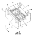
- FIGS. 2 and 3 Another prior art monolithic structure uses multilayer co-fired ceramic tape techniques and examples are shown in FIGS. 2 and 3 .
- the fabrication of these magnetic components, such as transformers, uses multiple layers of magnetic material and insulates the non-magnetic material to form a monolithic structure with well-defined magnetic and insulating non-magnetic regions. Windings can be formed using screen-printed conductors connected through the multilayer structure by conducting vias.
- Co-fired multilayer packages can be constructed with unfired green (dielectric) ceramic tape for the various layers.
- Compatible conductive compositions can use printed conductor layers interspersed between the dielectric layers, and interlayer connecting vias. The conductive layers are normally printed on the green tape, and the entire assembly is laminated and fired in one operation. It can reduce the physical size of circuitry and improve its reliability.
- FIGS. 2 and 3 The prior art examples shown in FIGS. 2 and 3 are explained in U.S. Patent No. 5,349,743 .
- Pluralities of the two ceramic green tape materials are layered with a desired geometry to form a laminated structure with well-defined magnetic and non-magnetic regions.
- Conducting paths are deposited on selected insulating non-magnetic tape layers. These conducting paths are connected by vias formed in the layers to create desired multi-turn windings for the magnetic component.
- the conducting paths can be constructed of a conductive material that is amenable to printing or other deposition techniques, and is compatible with the firing and sintering process characteristics of ferrite materials.
- Suitable conductive materials include palladium (Pd) or palladium-silver compositions (Pd-Ag) dispersed in an organic binder.
- Other suitable compositions include conductive metallic oxides (in a binder), which have the same firing and sintering characteristics as the ferrite materials used in constructing the magnetic devices.
- the structure formed by the layering technique is laminated under pressure and co-fired and sintered at a temperature of 1100 to 1400 degrees Centigrade to form a monolithic magnetic component structure having the desired electrical and magnetic properties.
- the Ni ferrite powder material is doped with Mn to a content equaling 1-10 mol% of the overall material composition.
- the component shown in FIG. 2 is constructed as a multiple winding transformer having a toroidal magnetic core structure.
- This toroidal core has four well-defined sections 31-34, each of which is constructed from a plurality of high permeability ceramic green tape layers.
- Sections 32 and 34 are circumscribed by conductive windings 35 and 36, respectively. Taken separately these windings form the primary and secondary windings of a transformer. If these windings are connected in series, however, the structure functions as a multiple turn inductor.
- Windings 35 and 36 can be formed by screen-printing pairs of conductor turns onto a plurality of insulating non-magnetic ceramic green tape layers. Each insulating non-magnetic layer can have suitable apertures for containing the sections of magnetic green tape layered inserts.
- the turns printed on each layer are connected to turns of the other layers with conductive vias 37, i.e., a through hole filled with a conductive material.
- Additional insulating non-magnetic layers are used to contain sections 31 and 33 of the magnetic tape sections and to form the top and bottom structure of the component.
- Conductive vias 38 are used to connect the ends of the windings 35 and 36 to connector pads 39 on the top surface of the component.
- the insulating non-magnetic regions of the structure are denoted by 40.
- Current excitation of the windings 35 and 36 produces a magnetic flux in the closed magnetic path defined by the sections 31-34 of the toroidal core.
- the fluxpath in this embodiment is in a vertical plane, e.g., the x-z plane shown in FIG.3 .
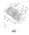
- FIG. 3 A phantom view of another prior art magnetic component is shown in FIG. 3 .
- This component as in the case with the prior example, is also constructed as a multiple winding transformer having a toroidal magnetic core structure.
- the toroidal core is defined by a main structure of magnetic material 41 positioned between top and bottom members 55 and 56, which are insulating non-magnetic material layers.
- Member 41 is further punctuated by inserts of insulating non-magnetic material inserts 42, 43, and 44, which provide support for conducting vias 61, which form part of the windings.
- the windings 51 and 52 are the primary and secondary, respectively, of the transformer.
- Windings 51 and 52 may be connected in series to form an inductor. These windings are formed by screen printing conductors on a layer of member 55 near the top of the structure and screen printing conductors on a layer of member 56 near the bottom of the structure and interconnecting these printed conductors with the conducting vias 61 to form the windings. Connector pads 57 are printed on the top surface of the top layer of member 58 and are connected by conducting vias 62 to the windings 51 and 52.
- FIGS. 4 and 11 Two different transformer structures are shown in FIGS. 4 and 11 , showing primary and secondary windings on a common core.
- FIG. 4 illustrates a transformer at 100 and shows a rectangular configured core 102 having an open area 104. The steps used for manufacturing the transformer 100 shown in FIG. 4 are shown in FIGS. 5-10 . Respective primary and secondary windings 106, 108 are illustrated.
- FIG. 5 is a plan view showing a substantially planar base 110 formed in this example as a substantially planar ceramic substrate for a fabrication sequence as a thick film substrate.
- a substantially planar configured, first half primary winding 112 is formed on the ceramic substrate 110. This winding can be typically formed by screen-printing a metallic conductor on the base 110, for example, a silver or gold screen-printed conductor.
- the base ceramic material could be an alumina type ceramic in one non-limiting example.
- an end 112a of the first half primary winding 112 extends beyond the other coil ends, and is operative as one of the connection points, i.e., terminals for the completed transformer 100. Standard photolithography techniques can be used for printing the metallic conductors.
- a ferrite paste 114 is applied to the first half primary winding 112 and over the base, leaving the ends exposed.
- the ferrite paste 114 could be an inorganic paste, for example, a ceramic slurry that includes ferrite-ceramic particles and a binder. It can later be fired for enhanced density and performance. This could be a low temperature system or a high temperature system depending on end-use designs. It is also possible to use tungsten or molybdenum. It should be understood that it is not necessary to fire at this step, although it is possible to conduct one or multiple firings throughout the process.
- the second half primary winding 120 is printed on the ferrite layer 114 such that the ends of this second half primary winding overlap the ferrite layer 114 and contact the exposed ends of the first half primary winding.
- One end 120a is longer and forms a terminal connection.
- the winding ends contact each other and form a completed transformer primary winding over the ferrite core formed by the ferrite paste 114.
- the line spacing can be about 2 to about 4 mils.
- the thick film process could be about one-half mil, e.g., about 12 microns, up to a thick film system norm of 0.05 to 0.10 mm (2 to about 4 mils). It should be understood that it is also possible to use a green tape system and vias.
- a dielectric layer 130 can be deposited over the second half primary winding 120 as illustrated.
- This dielectric layer 130 could be a glass material and similar structure and forms a cavity corresponding to the cavity 104 shown in FIG. 4 . It is also possible to use a material that burns-out and leaves a hole, as long as there is some structure left on which to print. The hole could be formed through evaporation in some manufacturing sequences.
- a first half secondary winding 140 is printed on the dielectric 130, and includes an end 140a that is operative as a terminal for the completed transformer.
- a second ferrite layer 150 is added as shown in FIG. 9 , and the second half secondary winding 160 is printed on the ferrite layer 150 such that its ends connect to the ends of the first half secondary winding 140 as shown in FIG. 10 .
- One end 160a is operative as a terminal for the completed transformer.
- the ferrite layer 150 is thick, the layer could be overprinted on the first half secondary winding 160.
- Conductive vias could be used to attach the first half secondary winding 140 and second half secondary winding 160.
- a coating or other layer could be applied subsequent to the step shown in FIG. 10 to aid in protecting the completed transformer structure.
- FIG. 11 A second example of a transformer is shown in FIG. 11 and has fabrication sequence steps shown in FIGS. 12-15 .
- This transformer design could be used for a mini S-band receiver operable at about 2.0 to about 4.0 GHz and designed to replace some commercial over-the-counter parts.
- the transformer is illustrated at 200 and includes a core 202 with a central portion 204 on which the primary and secondary transformer windings 206, 208 are wound.
- a base layer 210 can be formed as a green tape layer, for example, an LTCC structure, e.g., an unfired ferrite tape in one non-limiting example.
- a first half primary winding 212 is printed together with the first half secondary winding 214 and spaced between the "turns" or printed first half primary winding conductors. The conductors are spaced from each other such that the conductive metallic lines forming the first half secondary winding 214 are spaced from any conductive metallic lines forming the first half primary winding 212. Ends 212a, 214a are exposed, forming terminals for the primary and secondary windings.
- a ferrite layer 220 ( FIG. 13 ) forms a "wrap core" and is applied over the first half primary winding 212 and first half secondary winding 214.
- This ferrite layer 220 has conductor vias 222 formed therein, which could be formed as plated through-holes or punched holes filled with a conductive fill.
- a second half primary winding 230 and second half secondary winding 232 are printed on this ferrite "wrap core" 220 such that the winding ends connect to the conductive vias 222 and connect ends of the first half primary winding 212 and first half secondary winding 214. Longer ends of each winding 230, 232 form terminal ends 230a, 232a, as illustrated.
- a layer could be placed over the second half primary winding 230 and second half secondary winding 232 to leave only the ends exposed as illustrated in FIG. 15 . This layer could be a ferrite layer 250.
- any formed cavity is advantageous because the flux typically stays in the path of least reluctance. If some cavities are placed along edges lengthwise next to vias on the outside, it could improve the efficiency in some examples.
- FIG. 16 shows a flowchart and illustrates a sequence of steps used for making a transformer according to the present invention which is similar to that shown in FIG. 11 , using a liquid crystal polymer (LCP).
- the steps used for forming the transformer are similar to those signs shown in FIGS. 12-15 , but with a series of etching steps used instead.
- the liquid crystal polymer could be supplied in sheet form, in one non-limiting example, as a biaxially oriented film. It could include an orthogonal crystal structure as a biaxially oriented film. Ferrite fillers could be used to increase permeability and magnetic properties.
- the LCP sheets are preferably supplied as a laminate that includes a metallic cladding, for example, a copper cladding, which is etched to form a partial transformer structure similar to that shown in FIG. 12 with first half primary and secondary windings, followed by adding another LCP sheet and etching to form the second half primary and secondary windings.
- a metallic cladding for example, a copper cladding
- a first LCP layer is etched back (block 300) to form the first half primary and secondary windings.
- a ferrite layer is applied (block 302) and a second LCP layer applied and etched (block 304) to form the second half primary and secondary windings.
- the vias are formed (block 306) and a cover layer overlaid (block 308).
- the LCP sheets can be fused together such as in autoclave.
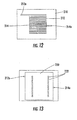
- FIG. 17 is a sectional view of the different layers that are used for forming the transformer using LCP's.
- the transformer structure 310 includes a first LCP layer 312 that includes an etched back LCP circuit layer 314 forming the first half primary and secondary windings.
- a ferrite layer 316 is added and followed by a second LCP layer 320 that includes an etched back LCP circuit layer 322 for the second half primary and secondary windings.
- Vias 324 connect between the LCP circuit layers 314, 322 interconnecting primary windings to each other and secondary windings to each other.
- a cover layer 326 can be added over the second LCP layer 320. This layer could also have an LCP circuit layer adjacent the ferrite in some instances depending on the processing sequences used.
- LCP has a unique property and can fuse to itself under pressure.
- An autoclave can be used to apply heat and pressure to allow the LCP sheets to fuse to themselves.
- a traditional prepeg process with plated through holes could also be used.
- the first half primary and first half secondary windings can be formed and another LCP sheet applied, which is etched back to form the second half primary and second half secondary windings.
- the vias can be drilled and plated or filled with conductive paste.
- the liquid crystal polymer is typically formed as a thermoplastic polymer material and has rigid and flexible monomers that link to each other.
- the segments align to each other in the direction of shear flow. Even when the LCP is cooled below a melting temperature, this direction and structure of orientation continues. This is different from most thermoplastic polymers where molecules are randomly oriented in a solid state.
- LCP has advantageous electrical, thermal, mechanical and chemical properties. It can be used for high-density printed circuit board (PCB) fabrication and semiconductor packaging. It can have a dielectric constant of about 3 in the range of about 0.5 to about 40 GHz and a low loss factor of about 0.004 and low moisture absorption and low moisture permeability.
- PCB printed circuit board
- LCP can be supplied as a thin film material ranging from about 25 micrometers to about 3 millimeters.
- One or both sides can include a copper cladding that is about 18 micrometers thick in some non-limiting examples, and could range even more.
- This copper cladding (layer) could be laminated in a vacuum press at around the melting point of LCP.
- Micromachining techniques could be used to allow MEMS applications. This could include photolithography, metallization, etching and electroplating. It is possible that some LCP material can be bonded to MEMS-related materials using a thermal bonding process and slight pressure at about the melting point or just below the melting point. Complex multilayer, three-dimensional structures could be formed.
Landscapes
- Engineering & Computer Science (AREA)
- Power Engineering (AREA)
- Manufacturing & Machinery (AREA)
- Microelectronics & Electronic Packaging (AREA)
- Chemical & Material Sciences (AREA)
- Ceramic Engineering (AREA)
- Inorganic Chemistry (AREA)
- Coils Or Transformers For Communication (AREA)
- Manufacturing Cores, Coils, And Magnets (AREA)
- Parts Printed On Printed Circuit Boards (AREA)
Claims (6)
- Verfahren zum Herstellen eines Transformators, das umfasst:- Ätzen erster halber primärer und sekundärer Windungen (300) als metallische Schaltungen auf einer metallischen Ummantelung einer ersten Flüssigkristallpolymer-(FKP-) Platte, so dass sekundäre Windungen in einem Abstandsverhältnis zu den primären Windungen positioniert sind,- Aufbringen einer Ferritschicht (302) auf die erste FKP-Platte in der Nähe der ersten halben primären und sekundären Windungen, um einen Umhüllungskern zu bilden,- Aufbringen einer zweiten FKP-Platte (302) auf die Ferritschicht, wobei sich die Ferritschicht zwischen der ersten und zweiten FKP-Platte befindet,- Ätzen zweiter halber primärer und sekundärer Windungen (304) als metallische Schaltungen auf einer metallischen Ummantelung der zweiten FKP-Platte,- Verschmelzen der ersten und zweiten FKP-Platte miteinander, um die Ferritschicht zwischen der ersten und zweiten FKP-Platte einzuhüllen, die die ersten und zweiten primären und sekundären Windungen tragen, und- Verbinden der jeweiligen ersten und zweiten halben primären Windungen und ersten und zweiten halben sekundären Windungen miteinander durch leitfähige Durchkontaktierungen (306).
- Verfahren nach Anspruch 1, das ferner das Ausbilden der leitfähigen Durchkontaktierungen als plattierte Durchgangslöcher umfasst.
- Verfahren nach Anspruch 1, das ferner das Ausstanzen von Löchern in den FKP-Platten und das Füllen der Löcher mit einem leitfähigen Füllmaterial zum Ausbilden der leitfähigen Durchkontaktierungen umfasst.
- Transformator mit:- einer ersten Flüssigkristallpolymer- (FKP-) Platte (312), die einander entgegengesetzte Seiten und eine metallische Ummantelung auf wenigstens einer der Seiten umfasst,- ersten halben primären und sekundären Windungen als metallische Schaltungen (314), die auf der metallischen Ummantelung geätzt sind,- einer zweiten FKP-Platte (320), die einander entgegengesetzte Seiten und eine metallische Ummantelung auf wenigstens einer der Seiten umfasst und auf die erste FKP-Platte aufgebracht ist,- zweiten halben primären und sekundären Windungen als metallische Schaltungen (322), die auf der metallischen Ummantelung der zweiten FKP-Platte geätzt sind,- einer Ferritschicht (316), die zwischen der ersten und zweiten FKP-Platte in der Nähe der ersten halben primären und sekundären Windungen positioniert ist, um einen Umhüllungskern zu bilden, der zwischen der ersten und zweiten FKP-Platte eingehüllt ist, die erste und zweite halbe primäre und sekundäre Windungen tragen, und- leitfähigen Durchkontaktierungen, die in der ersten und zweiten FKP-Platte ausgebildet sind und die jeweiligen ersten und zweiten halben primären Windungen und ersten und zweiten halben sekundären Windungen miteinander verbinden.
- Transformator nach Anspruch 4, wobei die leitfähigen Durchkontaktierungen als plattierte Durchgangslöcher ausgebildet sind.
- Transformator nach Anspruch 4, wobei die leitfähigen Durchkontaktierungen als ausgestanzte Löcher ausgebildet sind, die mit einem leitfähigen Füllmaterial gefüllt sind.
Applications Claiming Priority (2)
| Application Number | Priority Date | Filing Date | Title |
|---|---|---|---|
| US11/428,963 US7340825B2 (en) | 2006-07-06 | 2006-07-06 | Method of making a transformer |
| PCT/US2007/072763 WO2008005993A1 (en) | 2006-07-06 | 2007-07-03 | Transformer and associated method of making using liquid crystal polymer (lcp) material |
Publications (2)
| Publication Number | Publication Date |
|---|---|
| EP2044600A1 EP2044600A1 (de) | 2009-04-08 |
| EP2044600B1 true EP2044600B1 (de) | 2015-06-17 |
Family
ID=38582147
Family Applications (1)
| Application Number | Title | Priority Date | Filing Date |
|---|---|---|---|
| EP07799292.3A Active EP2044600B1 (de) | 2006-07-06 | 2007-07-03 | Transformator und entsprechendes herstellungsverfahren unter verwendung von flüssigkristallpolymer (lcp)-material |
Country Status (8)
| Country | Link |
|---|---|
| US (3) | US7340825B2 (de) |
| EP (1) | EP2044600B1 (de) |
| JP (1) | JP2009543361A (de) |
| KR (1) | KR101057567B1 (de) |
| CN (1) | CN101484957B (de) |
| CA (1) | CA2656644C (de) |
| TW (1) | TWI348718B (de) |
| WO (1) | WO2008005993A1 (de) |
Families Citing this family (9)
| Publication number | Priority date | Publication date | Assignee | Title |
|---|---|---|---|---|
| EP1864310A2 (de) * | 2005-03-02 | 2007-12-12 | Georgia Tech Research Corporation | Kapselungssysteme mit dünnfilm-flüssigkristallpolymer (lcp) und herstellungsverfahren |
| US8203418B2 (en) * | 2007-01-11 | 2012-06-19 | Planarmag, Inc. | Manufacture and use of planar embedded magnetics as discrete components and in integrated connectors |
| US7851039B2 (en) * | 2008-09-12 | 2010-12-14 | Faurecia Interior Systemns, Inc. | Decorative trim and method for making same |
| JP5409242B2 (ja) * | 2009-10-07 | 2014-02-05 | 新光電気工業株式会社 | インダクタ及びインダクタの製造方法 |
| CN103262187A (zh) * | 2011-02-15 | 2013-08-21 | 株式会社村田制作所 | 层叠型电感元件 |
| US10199152B2 (en) * | 2014-12-03 | 2019-02-05 | Qualcomm Incorporated | Embedded thin film magnetic carrier for integrated voltage regulator |
| KR20160102657A (ko) * | 2015-02-23 | 2016-08-31 | 삼성전기주식회사 | 칩 전자부품 및 그 제조방법 |
| US10236111B2 (en) * | 2017-04-12 | 2019-03-19 | Intel Corporation | Low-profile transformer and method of making same |
| US11715722B2 (en) * | 2020-04-30 | 2023-08-01 | Wolfspeed, Inc. | Wirebond-constructed inductors |
Family Cites Families (31)
| Publication number | Priority date | Publication date | Assignee | Title |
|---|---|---|---|---|
| US3614554A (en) * | 1968-10-24 | 1971-10-19 | Texas Instruments Inc | Miniaturized thin film inductors for use in integrated circuits |
| US3659240A (en) * | 1970-04-30 | 1972-04-25 | Bourns Inc | Thick-film electric-pulse transformer |
| GB8329957D0 (en) * | 1983-11-10 | 1983-12-14 | Ici Plc | Thermotropic polymer composition |
| JPS6119109A (ja) * | 1984-07-05 | 1986-01-28 | Nec Corp | トランス |
| US4876120A (en) | 1987-04-21 | 1989-10-24 | General Electric Company | Tailorable multi-layer printed wiring boards of controlled coefficient of thermal expansion |
| US4786120A (en) * | 1987-10-14 | 1988-11-22 | Casica Corporation | Keyboard enclosure assembly |
| JPH0227791A (ja) * | 1988-07-15 | 1990-01-30 | Shinto Paint Co Ltd | プリント回路基板の形成方法 |
| US5349743A (en) | 1991-05-02 | 1994-09-27 | At&T Bell Laboratories | Method of making a multilayer monolithic magnet component |
| US5393607A (en) * | 1992-01-13 | 1995-02-28 | Mitsui Toatsu Chemiclas, Inc. | Laminated transparent plastic material and polymerizable monomer |
| US5259110A (en) | 1992-04-03 | 1993-11-09 | International Business Machines Corporation | Method for forming a multilayer microelectronic wiring module |
| US5312674A (en) | 1992-07-31 | 1994-05-17 | Hughes Aircraft Company | Low-temperature-cofired-ceramic (LTCC) tape structures including cofired ferromagnetic elements, drop-in components and multi-layer transformer |
| US5696477A (en) * | 1994-05-30 | 1997-12-09 | Tabuchi Electric Co., Ltd. | Transformer |
| TW265450B (en) | 1994-06-30 | 1995-12-11 | At & T Corp | Devices using metallized magnetic substrates |
| US5719354A (en) | 1994-09-16 | 1998-02-17 | Hoechst Celanese Corp. | Monolithic LCP polymer microelectronic wiring modules |
| US6462976B1 (en) | 1997-02-21 | 2002-10-08 | University Of Arkansas | Conversion of electrical energy from one form to another, and its management through multichip module structures |
| US6007758A (en) | 1998-02-10 | 1999-12-28 | Lucent Technologies Inc. | Process for forming device comprising metallized magnetic substrates |
| TW410353B (en) | 1998-02-13 | 2000-11-01 | Thomson Brandt Gmbh | Transformer |
| JP2003321656A (ja) * | 2002-04-26 | 2003-11-14 | Japan Gore Tex Inc | 高接着性液晶ポリマーフィルム |
| JP3969192B2 (ja) | 2002-05-30 | 2007-09-05 | 株式会社デンソー | 多層配線基板の製造方法 |
| JP2004082564A (ja) * | 2002-08-28 | 2004-03-18 | Kuraray Co Ltd | 電子デバイスの支持体 |
| KR100755088B1 (ko) | 2003-03-28 | 2007-09-03 | 티디케이가부시기가이샤 | 다층 기판 및 그 제조방법 |
| TW573444B (en) * | 2003-04-22 | 2004-01-21 | Ind Tech Res Inst | Substrate having organic and inorganic functional package |
| US7005955B2 (en) | 2003-04-23 | 2006-02-28 | Hewlett-Packard Development Company, L.P. | Inductor or transformer having a ferromagnetic core that is formed on a printed circuit board |
| JP2005039187A (ja) * | 2003-06-26 | 2005-02-10 | Murata Mfg Co Ltd | 積層コイル部品 |
| US6933596B2 (en) * | 2003-07-01 | 2005-08-23 | Northrop Grumman Corporation | Ultra wideband BGA |
| EP1661148A2 (de) * | 2003-08-26 | 2006-05-31 | Philips Intellectual Property & Standards GmbH | Leiterplatte mit integrierter induktivität |
| US6990729B2 (en) * | 2003-09-05 | 2006-01-31 | Harris Corporation | Method for forming an inductor |
| DE602005002547T2 (de) | 2004-02-23 | 2008-06-12 | Georgia Tech Research Corp. | Passive signalverarbeitungskomponenten auf flüssigkristallpolymer- und mehrschichtpolymerbasis für hf-/drahtlos-mehrband-anwendungen |
| JP2006049536A (ja) * | 2004-08-04 | 2006-02-16 | Sohki:Kk | 多層回路基板 |
| JP4648668B2 (ja) * | 2004-08-31 | 2011-03-09 | ニチハ株式会社 | 無機質板およびその製造方法 |
| US8350657B2 (en) * | 2005-06-30 | 2013-01-08 | Derochemont L Pierre | Power management module and method of manufacture |
-
2006
- 2006-07-06 US US11/428,963 patent/US7340825B2/en active Active
-
2007
- 2007-07-03 KR KR1020097002537A patent/KR101057567B1/ko not_active Expired - Fee Related
- 2007-07-03 CA CA2656644A patent/CA2656644C/en not_active Expired - Fee Related
- 2007-07-03 JP JP2009518618A patent/JP2009543361A/ja active Pending
- 2007-07-03 EP EP07799292.3A patent/EP2044600B1/de active Active
- 2007-07-03 CN CN2007800256459A patent/CN101484957B/zh not_active Expired - Fee Related
- 2007-07-03 WO PCT/US2007/072763 patent/WO2008005993A1/en not_active Ceased
- 2007-07-05 TW TW096124513A patent/TWI348718B/zh active
- 2007-08-15 US US11/838,911 patent/US7509727B2/en active Active
- 2007-08-15 US US11/838,921 patent/US7391293B2/en active Active
Also Published As
| Publication number | Publication date |
|---|---|
| CN101484957B (zh) | 2012-04-18 |
| WO2008005993A1 (en) | 2008-01-10 |
| KR20090030335A (ko) | 2009-03-24 |
| CN101484957A (zh) | 2009-07-15 |
| US7509727B2 (en) | 2009-03-31 |
| TW200811890A (en) | 2008-03-01 |
| CA2656644C (en) | 2012-12-04 |
| CA2656644A1 (en) | 2008-01-10 |
| JP2009543361A (ja) | 2009-12-03 |
| US20080007383A1 (en) | 2008-01-10 |
| EP2044600A1 (de) | 2009-04-08 |
| TWI348718B (en) | 2011-09-11 |
| KR101057567B1 (ko) | 2011-08-17 |
| US7340825B2 (en) | 2008-03-11 |
| US7391293B2 (en) | 2008-06-24 |
| US20080007380A1 (en) | 2008-01-10 |
| US20080005890A1 (en) | 2008-01-10 |
Similar Documents
| Publication | Publication Date | Title |
|---|---|---|
| US7449987B2 (en) | Transformer and associated method of making | |
| EP2044600B1 (de) | Transformator und entsprechendes herstellungsverfahren unter verwendung von flüssigkristallpolymer (lcp)-material | |
| JP4969242B2 (ja) | 内蔵トロイダルインダクタ | |
| CN106328339B (zh) | 线圈部件 | |
| CA2560697C (en) | Embedded toroidal transformers in ceramic substrates | |
| CA2597058C (en) | Embedded toroidal inductor | |
| KR100243356B1 (ko) | 적층세라믹트랜스포머및그제조방법 | |
| KR0121767Y1 (ko) | 다층 하이브리드회로 |
Legal Events
| Date | Code | Title | Description |
|---|---|---|---|
| PUAI | Public reference made under article 153(3) epc to a published international application that has entered the european phase |
Free format text: ORIGINAL CODE: 0009012 |
|
| 17P | Request for examination filed |
Effective date: 20090205 |
|
| AK | Designated contracting states |
Kind code of ref document: A1 Designated state(s): AT BE BG CH CY CZ DE DK EE ES FI FR GB GR HU IE IS IT LI LT LU LV MC MT NL PL PT RO SE SI SK TR |
|
| AX | Request for extension of the european patent |
Extension state: AL BA HR MK RS |
|
| 17Q | First examination report despatched |
Effective date: 20090507 |
|
| DAX | Request for extension of the european patent (deleted) | ||
| RBV | Designated contracting states (corrected) |
Designated state(s): DE FI FR GB SE |
|
| GRAP | Despatch of communication of intention to grant a patent |
Free format text: ORIGINAL CODE: EPIDOSNIGR1 |
|
| INTG | Intention to grant announced |
Effective date: 20150205 |
|
| GRAS | Grant fee paid |
Free format text: ORIGINAL CODE: EPIDOSNIGR3 |
|
| GRAA | (expected) grant |
Free format text: ORIGINAL CODE: 0009210 |
|
| AK | Designated contracting states |
Kind code of ref document: B1 Designated state(s): DE FI FR GB SE |
|
| REG | Reference to a national code |
Ref country code: GB Ref legal event code: FG4D |
|
| REG | Reference to a national code |
Ref country code: DE Ref legal event code: R096 Ref document number: 602007041805 Country of ref document: DE |
|
| PG25 | Lapsed in a contracting state [announced via postgrant information from national office to epo] |
Ref country code: FI Free format text: LAPSE BECAUSE OF FAILURE TO SUBMIT A TRANSLATION OF THE DESCRIPTION OR TO PAY THE FEE WITHIN THE PRESCRIBED TIME-LIMIT Effective date: 20150617 |
|
| REG | Reference to a national code |
Ref country code: DE Ref legal event code: R097 Ref document number: 602007041805 Country of ref document: DE |
|
| PLBE | No opposition filed within time limit |
Free format text: ORIGINAL CODE: 0009261 |
|
| STAA | Information on the status of an ep patent application or granted ep patent |
Free format text: STATUS: NO OPPOSITION FILED WITHIN TIME LIMIT |
|
| 26N | No opposition filed |
Effective date: 20160318 |
|
| REG | Reference to a national code |
Ref country code: FR Ref legal event code: PLFP Year of fee payment: 10 |
|
| PG25 | Lapsed in a contracting state [announced via postgrant information from national office to epo] |
Ref country code: SE Free format text: LAPSE BECAUSE OF FAILURE TO SUBMIT A TRANSLATION OF THE DESCRIPTION OR TO PAY THE FEE WITHIN THE PRESCRIBED TIME-LIMIT Effective date: 20150617 |
|
| REG | Reference to a national code |
Ref country code: FR Ref legal event code: PLFP Year of fee payment: 11 |
|
| REG | Reference to a national code |
Ref country code: FR Ref legal event code: PLFP Year of fee payment: 12 |
|
| P01 | Opt-out of the competence of the unified patent court (upc) registered |
Effective date: 20230530 |
|
| PGFP | Annual fee paid to national office [announced via postgrant information from national office to epo] |
Ref country code: DE Payment date: 20240729 Year of fee payment: 18 |
|
| PGFP | Annual fee paid to national office [announced via postgrant information from national office to epo] |
Ref country code: GB Payment date: 20240729 Year of fee payment: 18 |
|
| PGFP | Annual fee paid to national office [announced via postgrant information from national office to epo] |
Ref country code: FR Payment date: 20240725 Year of fee payment: 18 |
|
| REG | Reference to a national code |
Ref country code: DE Ref legal event code: R119 Ref document number: 602007041805 Country of ref document: DE |
|
| GBPC | Gb: european patent ceased through non-payment of renewal fee |
Effective date: 20250703 |