EP2043139A2 - Method of preventing etch profile bending and bowing in high aspect ratio openings by treating a polymer formed on the opening sidewalls - Google Patents
Method of preventing etch profile bending and bowing in high aspect ratio openings by treating a polymer formed on the opening sidewalls Download PDFInfo
- Publication number
- EP2043139A2 EP2043139A2 EP08165173A EP08165173A EP2043139A2 EP 2043139 A2 EP2043139 A2 EP 2043139A2 EP 08165173 A EP08165173 A EP 08165173A EP 08165173 A EP08165173 A EP 08165173A EP 2043139 A2 EP2043139 A2 EP 2043139A2
- Authority
- EP
- European Patent Office
- Prior art keywords
- bias power
- flow rate
- polymer film
- power level
- gas
- Prior art date
- Legal status (The legal status is an assumption and is not a legal conclusion. Google has not performed a legal analysis and makes no representation as to the accuracy of the status listed.)
- Withdrawn
Links
Images


Classifications
-
- H10P50/242—
-
- H10P50/283—
-
- H—ELECTRICITY
- H01—ELECTRIC ELEMENTS
- H01J—ELECTRIC DISCHARGE TUBES OR DISCHARGE LAMPS
- H01J37/00—Discharge tubes with provision for introducing objects or material to be exposed to the discharge, e.g. for the purpose of examination or processing thereof
- H01J37/32—Gas-filled discharge tubes
- H01J37/32009—Arrangements for generation of plasma specially adapted for examination or treatment of objects, e.g. plasma sources
- H01J37/32082—Radio frequency generated discharge
- H01J37/32091—Radio frequency generated discharge the radio frequency energy being capacitively coupled to the plasma
-
- H—ELECTRICITY
- H01—ELECTRIC ELEMENTS
- H01J—ELECTRIC DISCHARGE TUBES OR DISCHARGE LAMPS
- H01J37/00—Discharge tubes with provision for introducing objects or material to be exposed to the discharge, e.g. for the purpose of examination or processing thereof
- H01J37/32—Gas-filled discharge tubes
- H01J37/32009—Arrangements for generation of plasma specially adapted for examination or treatment of objects, e.g. plasma sources
- H01J37/32082—Radio frequency generated discharge
- H01J37/32137—Radio frequency generated discharge controlling of the discharge by modulation of energy
-
- H—ELECTRICITY
- H01—ELECTRIC ELEMENTS
- H01J—ELECTRIC DISCHARGE TUBES OR DISCHARGE LAMPS
- H01J37/00—Discharge tubes with provision for introducing objects or material to be exposed to the discharge, e.g. for the purpose of examination or processing thereof
- H01J37/32—Gas-filled discharge tubes
- H01J37/32431—Constructional details of the reactor
- H01J37/3244—Gas supply means
- H01J37/32449—Gas control, e.g. control of the gas flow
-
- H10W20/081—
Definitions
- Embodiments of the present invention pertain to semiconductor device fabrication, and in particular to plasma etch processes employed in semiconductor device fabrication. Further, the present invention relates to a method of performing plasma ion etching to form a high aspect ratio contact opening in a dielectric layer on a substrate.
- Microelectronic device fabrication on a semiconductor wafer requires formation of openings through dielectric thin film layers that are adapted to be filled with metal to provide electrical contact between conductors in different layers.
- the contact openings typically have an aspect ratio (depth-to-diameter ratio) as high as 40:1.
- aspect ratio depth-to-diameter ratio
- the hole diameter of a contact opening may be reduced to about 630 ⁇ , while the required depth is about 24,700 ⁇ .
- the opening diameter and the opening-to-opening spacing may be about the same (e.g., roughly 630 ⁇ ).
- the contact opening location pattern and diameter is defined by an aperture in a patterned photoresist layer that is deposited on the wafer surface prior to formation of the openings.
- Each photoresist aperture defines a contact opening location and diameter.
- the contact openings are formed by a plasma etch process that is adapted to etch dielectric material through the apertures in the photoresist layer.
- the plasma etch process employs a fluorocarbon/ fluorohydrocarbon gas that produces two types of species in the plasma: etch species having high fluorine-to-carbon content ratio, and polymer species having a high carbon-to-fluorine content ratio.
- the polymer species accumulates on exposed surfaces of the sidewall of each opening, which enhances etch selectivity and can reduce the tendency of the etch process to widen the opening beyond the diameter established by the photoresist pattern.
- Etch profile is controlled by chamber pressure and by RF bias power. Increasing the RF bias power produces straighter and narrower etch profiles by increasing the ion energy and momentum in the vertical direction. Reducing the chamber pressure can have a similar effect by reducing collisions with ions, thereby reducing the number of ions deflected from their nominal vertical trajectory.
- bowing is manifested by a widened section of the contact opening near the top of the opening.
- the diameter of the widened section may be as much as twice the desired hole diameter, increasing the likelihood of partial merging of adjacent openings at the widened section.
- Another problem, referred to herein as "bending”, is manifested by a deflection of the axis of the opening away from true vertical near the bottom of the opening. Such bending has been observed to deflect the center of the opening bottom toward its neighbor by as much as 50% to 100% of the opening diameter.
- a method for performing plasma ion etching of high aspect ratio contact openings in a dielectric layer on a substrate includes introducing into the plasma reactor chamber a fluorocarbon and/or fluorohydrocarbon gas such as C 2 F 4 , C 4 F 6 , CH 2 F 2 or C 4 F 8 at a first gas flow rate, silicon fluoride gas at a second flow rate that is within a factor between 0.5 and 1.5, in particular 0.75 to 1.25, of the first flow rate, and Argon gas at a flow rate that is a factor between about 2 and 7 times, in particular between about 4 and 6 times, the first flow rate.
- a fluorocarbon and/or fluorohydrocarbon gas such as C 2 F 4 , C 4 F 6 , CH 2 F 2 or C 4 F 8
- silicon fluoride gas at a second flow rate that is within a factor between 0.5 and 1.5, in particular 0.75 to 1.25, of the first flow rate
- Argon gas at a flow rate that is a factor between about 2 and 7
- the method further includes etching a contact opening in the dielectric layer while depositing a polymer film on a side wall of the contact opening having a film thickness less than the radius of the contact opening.
- etching a contact opening in the dielectric layer while depositing a polymer film on a side wall of the contact opening is done by coupling RF power into the chamber to generate a plasma in the chamber while continuously applying RF bias power of a nominal RF bias power level corresponding to a desired plasma etch process.
- the conductivity of the polymer film on the side wall is increased by using conductive polymer material and by ion bombardment of the polymer film with Argon ions, and by coupling to the substrate successive bursts of RF bias power of a high RF bias power level in excess of more than 1.5 times the nominal power level.
- Embodiments are also directed to apparatuses for carrying out the disclosed methods and including apparatus parts for performing described method steps. Furthermore, embodiments are also directed to methods by which the described apparatus operates or by which the described apparatus is manufactured. It may include method steps for carrying out functions of the apparatus or manufacturing parts of the apparatus. The method steps may be performed by way of hardware components, firmware, software, a computer programmed by appropriate software, by any combination thereof or in any other manner.
- high aspect ratio contact openings are etched while preventing bowing or bending of the etch profile by forming a highly conductive thin film on the side wall of each contact opening.
- the conductivity of the thin film on the side wall is enhanced by ion bombardment carried out periodically during the etch process.
- FIG. 1 depicts the effects of static charge accumulation in a high aspect ratio contact opening during the contact etch process.
- FIG. 2 is a graph illustrating the angular velocity distribution at the wafer surface of ion trajectories (solid line) and electron trajectories (dashed line).
- FIG. 3 is a graph of the ion energy distribution.
- FIG. 4 depicts the resulting etch profile of high aspect ratio contact openings caused by the charge accumulation effects depicted in FIG. 1 .
- FIG. 5 illustrates a concept in accordance with an embodiment in which a conductive film covers the side walls of the high aspect ratio openings.
- FIG. 6 depicts the final etch profile achieved in a plasma etch process of the type depicted in FIG. 5 .
- FIG. 7 depicts electrical discharge time as a function of conductivity in a partially conductive polymer film.
- FIGS. 8A through 8H depict a chronological succession of etch profiles obtained during a plasma etch process in accordance with one embodiment.
- FIG. 9 depicts the applied RF bias power level as a function of time in the process of FIG. 8 .
- FIG. 10 depicts a plasma reactor configured to carry out the etch process of FIG. 5 .
- FIG. 11 is a flow chart corresponding to a process in accordance with one embodiment.
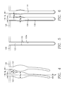
- a high aspect ratio contact opening 100 is formed in a dielectric film 102 in registration with an aperture 104 through an overlying photoresist layer 106.
- the opening 100 is formed by the reaction of the exposed portion of the dielectric film 102 with etchant species in a fluorocarbon/ fluorohydrocarbon plasma 108. Both electrons and positively charged ions from the plasma encounter the sidewall 100a of the opening 100. As shown in the graph of FIG.
- the ions have a narrow angular velocity distribution or profile (solid line) concentrated about the vertical direction relative to the top surface of the dielectric layer 102, while the electrons have a more isotropic angular velocity distribution.
- virtually no electrons from the plasma are able to travel to the bottom of the high aspect ratio opening 100 before being absorbed by collisions with the side wall 100a. Instead, nearly all the electrons are absorbed by collisions with the top portion of the side wall 100a, so that the top portion of the side wall 100a becomes negatively charged.
- the ions have two energy peaks.
- a high energy peak occurs at an ion energy corresponding to the peak-to-peak voltage of the RF bias signal applied to the wafer.
- a lower energy peak occurs at an ion energy corresponding to one-half of the peak-to-peak bias voltage.
- the ion population distribution at the various kinetic energy levels is depicted in the graph of FIG. 3 .
- the higher energy peak increases in population as the RF frequency of the bias signal decreases.
- the higher energy ions tend not to collide with the side wall 100a until they reach the bottom portion of the opening 100, so that the bottom portion of the side wall 100a becomes positively charged.
- the lower energy ions are more easily deflected from their vertical trajectory by negative charge that accumulates near the top of the side wall 100a.
- the deflected ion path 112 depicted in FIG. 1 represents a typical path of a lower energy ion which is deflected from true vertical as the ion travels in a curved path through the electric field of the negatively charged section of the side wall 100a, the deflected ion path eventually intersecting the side wall 100a at a point below the negatively charged section of the side wall 100a. This increases the etch rate of the side wall 102 at that point, leading to bowing of the opening profile in the region near the intersection of the deflected ion path and the side wall 100a. The result is depicted in FIG.
- a high aspect ratio contact opening 100 having a nominal diameter D has a section near its top with an enlarged diameter D B representing the bowing of the etch profile.
- the contact opening 100 is separated from an adjacent contact opening 101 by a nominal separation distance S 1 .
- the separation distance decreases to a small separation S 2 , which may be as little as 5% of the nominal separation distance S 1 .
- the separation, S 2 may be zero in the vicinity of the bowing.
- the enlarged opening diameter D B may be nearly twice the nominal diameter D.
- the bending problem arises because of uneven charge distribution around the circumference of the side wall 100a. This may be an uneven circumferential distribution of the positive charge that accumulates near the bottom of the opening 100, for example. Such uneven charge distribution produces a small net deflection of the higher energy ions that is not manifested until the ions have traveled a sufficiently long distance, or to the bottom of the opening 100. As a result, the bending problem appears as a lateral shift in the position of the center of the bottom of the opening 100 from the center (or axis) of the top of the opening 100. Referring to FIG. 4 , the bottom of the opening 100 is laterally shifted by a bending distance B that is about equal to the diameter D of the opening.
- Embodiments of the present invention pertain to solving both the bowing problem and the bending problem by providing, during the entire duration of the plasma etch process, a conductive thin film on the side wall 100a of each opening 100.
- the conductive coating constitutes an electrical discharge path along which uneven distribution of charge may flow so as to equilibrate the charge distribution.
- build-up of negative charge near the top of the opening 100 and positive charge near the bottom of the opening 100 is reduced or eliminated by the positive and negative charges flowing toward one another along the conductive thin film on the side wall 100a.
- the depth of the opening 100 constantly increases, lengthening the depth of the side wall 100a. As the depth of the opening 100 increases during the etch process to constantly form an additional section of side wall 100a, the conductive thin film is extended downwardly to coat the additional section. In one embodiment, the process is carried on continually during the etch process.
- FIG. 5 depicts the beginning of a contact opening 100 near the start of the etch process, showing a conductive thin film 130 coating the side wall 100a.
- FIG. 6 depicts the results of this process after the contact opening 100 has reached its full depth, about 24,700 ⁇ .
- the diameter D B at the bow is within 10% or less of the nominal diameter D.
- the bending distance B (the deflection of the opening axis at the bottom) has been reduced to nearly zero.
- the conductive thin film 130 is formed by employing a fluorocarbon and/or fluorohydrocarbon process gas of either C 2 F 4 , C 4 F 6 , CH 2 F 2 or C 4 F 8 during the plasma etch process.
- Fluorine-rich plasma by-products formed by dissociation of the fluorocarbon/ fluorohydrocarbon gas molecules in the plasma etch the exposed portion of the dielectric material 102.
- Carbon-rich plasma by-products formed by dissociation of the fluorocarbon/ fluorohydrocarbon gas molecules in the plasma tend to deposit on the side wall 100a as the thin conductive polymer layer 130 which is on the order of about 10 ⁇ thick.
- FIG. 7 is a graph depicting the 1/e discharge time (vertical axis) as function of conductivity (horizontal axis) for a given dielectric constant that is typical of a fluorocarbon polymer of the type discussed above.
- the conductive layer 130 is a specially formed polymer that has both dielectric and conductive properties, with a sufficient conductivity to minimize the 1/e discharge time to on the order of 10 -11 sec or less.
- the effect of providing such conductivity in the layer 130 is to cause the positive and negative charges on the side wall 100a or (more accurately) in the layer 130 to flow toward one another and thereby neutralize or equilibrate. The result is a uniform distribution of static charge along the side wall 100a, or possibly a cancellation of static charge.
- a conductive polymer is formed by employing, for example, either C 2 F 4 , C 4 F 6 , CH 2 F 2 or C 4 F 8 as the process gas during the plasma etch process in which the contact opening 100 of FIG 6 is formed.
- C 2 F 4 , C 4 F 6 , CH 2 F 2 or C 4 F 8 forms polymer precursors in the plasma that tend to form a conductive polymer when deposited on the side wall 100a as the conductive layer 130.
- the requisite conductivity is attained by adding a semiconductor species-containing process gas into the plasma, such as SiF 4 silicon fluoride. This causes the polymer layer 130 to include silicon atoms in the polymer structure, increasing the conductivity of the polymer layer 130.
- conductivity of the polymer layer 130 on the side wall 100a is further enhanced by adding a relatively high atomic number inert gas, such as Argon, into the plasma and ion bombarding the polymer layer 130 with high energy Argon ions.
- a relatively high atomic number inert gas such as Argon
- the result can be to transform the molecular structure of the polymer film 130 so that it becomes more like a graphite structure.
- the graphite structure is a planar hexagonal carbon crystal structure with high electrical conductivity.
- Argon ion bombardment is carried out at a sufficient ion energy to attain a conductivity of about 5 S/m in the polymer layer 130.
- the high power high voltage RF bias required for the Argon ion bombardment may be incompatible with some dielectric etch process recipes.
- the Argon ion bombardment is performed periodically in short bursts/flashes so as to have less effect on the plasma etch process, leaving the RF bias power at a lower level that is compatible with the etch process recipe, except during each short burst when high energy Argon ion bombardment is performed.
- FIGS. 8A through 8H are a chronological succession of etch profile images depicting the progressive etching of a contact opening.
- FIGS. 8A through 8H only the portion of the conductive layer that has been previously exposed to high energy Argon ion bombardment is shaded, the unshaded portion representing a new portion of the conductive layer 130 formed since the previous ion bombardment burst and therefore not yet exposed to ion bombardment.
- FIGS. 8A, 8C, 8E, 8G a new section of side wall 100a and new section of polymer film 130 (unshaded) has been formed in the interim between successive bursts so that it has not yet been exposed to a high bias power.
- FIGS. 8A, 8C, 8E, 8G a new section of side wall 100a and new section of polymer film 130 (unshaded) has been formed in the interim between successive bursts so that it has not yet been exposed to a high bias power.
- the RF bias power remains at a nominal power level called for by the etch process recipe (e.g., 3 kiloWatts or in a range of 500 Watts to 4 kiloWatts, in particular 1 kiloWatts to 3 kiloWatts), except for short periodic bursts, during which the power is temporarily raised to a high level (e.g., 6 kiloWatts).
- the RF power level may be pulsed in bursts, as depicted in FIG. 9 , but the Argon gas flow rate may be constant. Fluorocarbon or fluorohydrocarbon process gases are used during nominal etch, while Ar only during Ar bursts.
- the duration of each burst is sufficient to attain the required increase in electrical conductivity in the newly exposed portion of the polymer film 130, and may be on the order of 10 millisecond (e.g., in a range of about 0.25 ms to 1 sec or more).
- the difference may be relatively high in the case of a nominal etch process bias power level (e.g., 500 W) and an ion bombardment burst of 6 kW, in which case the duration of each 6 kW burst should be relatively short, e.g., about 1 ms.
- the difference is less, and therefore the burst duration may be increased above 10 ms to on the order of 1 second, for example.
- the time between bursts is sufficiently short to prevent significant charge build-up in the new (unshaded) portion of the polymer film 130 not yet exposed to the high energy ion bombardment, and may be on the order of one second (e.g., 0.5 seconds to 5 seconds).
- the RF bias signal frequency is an LF frequency in the range of 1-4 MHz, for example.
- a 13.56 MHz RF bias power component may also be applied to the wafer.
- the chamber pressure has a wider range than in conventional processes, and may be set anywhere between 10 milliTorr and 1 Torr, in particular 200 milliTorr and 800 milliTorr.
- the bowing and bending problem is reduced or eliminated by charge neutralization (or equilibration) through the conductive layer 130, so that some increase in angular deflection of ion trajectory from the vertical direction (due to an increase in chamber pressure) may be tolerated.
- the density of the plasma is controlled by coupling RF plasma source power into the chamber from an RF source power applicator, which may be an inductive coil or an overhead capacitive electrode.
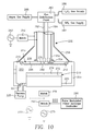
- FIG. 10 A plasma reactor adapted to carry out the foregoing process is depicted in FIG. 10 .
- the reactor includes a vacuum chamber 200 enclosed by a cylindrical side wall 205, a ceiling 210, an overhead electrode 215 in an aperture of the ceiling 210, and a floor 220.
- An insulating ring 212 separates the electrode 215 from the ceiling 210.
- a vacuum pump 225 is coupled to the chamber 200 through a pumping port 227 in the floor 220.
- the overhead electrode 215 is a gas distribution plate having inner and outer interior gas manifolds 230, 235 that feed inner and outer arrays of gas injection orifices 240, 245.
- a coaxial RF feed structure 250 couples RF plasma source power to the overhead electrode 215, the feed structure 250 including an inner hollow cylindrical conductor 252 coupled to the electrode 215 through a thin insulating ring 254, and an outer hollow cylindrical conductor 256 terminated at the ceiling 210.
- An RF source power generator 260 is coupled to the inner and outer coaxial conductors 252, 256 through a fixed impedance match element 262 which may be a coaxial tuning stub.
- a wafer support pedestal 270 includes an insulating layer 272 enclosing a cathode electrode 274 that is coupled to an RF bias power generator 276 through an impedance match element 278.
- a process gas distribution panel 280 supplies process gas to the inner and outer manifolds 230, 235 through gas supply lines 282, 284.
- Various gas supplies are coupled to the gas distribution panel, including a fluorocarbon/ fluorohydrocarbon gas supply 286, a silicon fluoride gas supply 287 and an Argon gas supply 288.
- the gas distribution panel 280 determines the flow rates of the individual gases that constitute the total gas flow rate in the gas supply lines 282, 284.
- a pulse modulated power envelope controller 290 enables the generator 276 to apply high power bursts (e.g., 6 kW) while maintaining a nominal power output level (e.g., 3 kW) between bursts.
- the controller 290 may control a switch 292 at the output of the generator 276.
- a second generator 277 (shown in dashed line) supplies the constant nominal (e.g., 3 kiloWatt) power output, while the generator 276 supplies the periodic short 6 kW bursts that are gated by the switch 292.
- each of the periodic high power bursts is sufficiently short to minimize impact on the etch process recipe, but is sufficiently long to obtain an increase in conductivity of the polymer film 130 of FIG. 5 .
- the time between bursts is sufficiently short to prevent significant static charge build-up on the contact opening side wall 100a of FIG. 8 .
- newly formed portions of the polymer layer 130 of FIG. 8 have not been exposed to ion bombardment and therefore have a lower conductivity, thereby rendering the new portions susceptible to charge accumulation. This accumulation can be minimized (to avoid bowing or bending of the etch profile) by minimizing the time between bursts of high power RF bias on the wafer.
- each high power RF bias burst may be, for example, about 10 ms, and the time between bursts may be about 1 sec.
- the fluorocarbon/ fluorohydrocarbon process gas flow rate may be in the range of 10-100 sccm to the combination of the inner and outer gas manifolds 230, 235.
- the Argon flow rate is about 2 to 7 times the fluorocarbon/ fluorohydrocarbon gas flow rate.
- the silicon fluoride flow rate is between about 0.5 and 1.5 times the flow rate of the fluorocarbon/ fluorohydrocarbon process gas.
- the nominal bias power level may be about 500-4000 Watts while the RF burst level may be in the range of about 5-10 kiloWatts.
- the bias power frequency may be in the range of 1-4 MHz.
- the chamber pressure may be in the range of 1 milliTorr to 10 Torr, for example, in particular in the range of 0.5 Torr to 5 Torr.
- the fluorocarbon process gas may be C 2 F 4 .
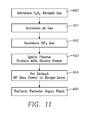
- FIG. 11 illustrates a process in accordance with one embodiment.
- a fluorocarbon/ fluorohydrocarbon gas e.g., C 2 F 4 , C 4 F 6 , CH 2 F 2 or C 4 F 8
- a flow rate in a range of 10-100 sccm (block 400).
- Ar gas is introduced (block 401) at a flow rate (e.g., 300-750 sccm) between 2 and 7 times the fluorocarbon/ fluorohydrocarbon gas flow rate and silicon fluoride gas is introduced at a flow rate (e.g., 10-100 sccm) between 0.5 and 1.5 times the flow rate of the fluorocarbon/ fluorohydrocarbon gas (block 402).
- RF source power is applied and RF bias power is applied to ignite a plasma in the chamber.
- the RF bias power level is set to a nominal level called for by an etch process recipe, for example 500-4000 Watts, at which acceptable etch selectivity and minimal photoresist faceting or damage is experienced.
- etch process recipe for example 500-4000 Watts
- the bias power is periodically increased to about 6 kW for a brief period of time (e.g., 10 msec) with Ar flow only at a predetermined rate (e.g., once every second). This is carried out until the contact opening has been etched to the desired depth.
Landscapes
- Physics & Mathematics (AREA)
- Engineering & Computer Science (AREA)
- Plasma & Fusion (AREA)
- Chemical & Material Sciences (AREA)
- Analytical Chemistry (AREA)
- Drying Of Semiconductors (AREA)
- Plasma Technology (AREA)
- Electrodes Of Semiconductors (AREA)
- Internal Circuitry In Semiconductor Integrated Circuit Devices (AREA)
Applications Claiming Priority (1)
| Application Number | Priority Date | Filing Date | Title |
|---|---|---|---|
| US11/861,032 US7846846B2 (en) | 2007-09-25 | 2007-09-25 | Method of preventing etch profile bending and bowing in high aspect ratio openings by treating a polymer formed on the opening sidewalls |
Publications (1)
| Publication Number | Publication Date |
|---|---|
| EP2043139A2 true EP2043139A2 (en) | 2009-04-01 |
Family
ID=39952217
Family Applications (1)
| Application Number | Title | Priority Date | Filing Date |
|---|---|---|---|
| EP08165173A Withdrawn EP2043139A2 (en) | 2007-09-25 | 2008-09-25 | Method of preventing etch profile bending and bowing in high aspect ratio openings by treating a polymer formed on the opening sidewalls |
Country Status (6)
| Country | Link |
|---|---|
| US (1) | US7846846B2 (enExample) |
| EP (1) | EP2043139A2 (enExample) |
| JP (1) | JP5553496B2 (enExample) |
| KR (1) | KR101019930B1 (enExample) |
| CN (1) | CN101447425B (enExample) |
| TW (1) | TWI367527B (enExample) |
Cited By (1)
| Publication number | Priority date | Publication date | Assignee | Title |
|---|---|---|---|---|
| EP2056341A3 (en) * | 2007-11-02 | 2010-03-03 | Applied Materials, Inc. | Methods for forming high aspect ratio features on a substrate |
Families Citing this family (13)
| Publication number | Priority date | Publication date | Assignee | Title |
|---|---|---|---|---|
| KR101575190B1 (ko) * | 2010-02-12 | 2015-12-08 | 삼성전자주식회사 | 윗면과 바닥면의 시디차가 없는 깊은 트렌치를 갖는 반도체 및 제조방법 |
| CN101866848B (zh) * | 2010-04-29 | 2012-05-30 | 中微半导体设备(上海)有限公司 | 一种刻蚀有机物层的等离子刻蚀方法 |
| US9165785B2 (en) | 2013-03-29 | 2015-10-20 | Tokyo Electron Limited | Reducing bowing bias in etching an oxide layer |
| US9275869B2 (en) * | 2013-08-02 | 2016-03-01 | Lam Research Corporation | Fast-gas switching for etching |
| KR102203460B1 (ko) | 2014-07-11 | 2021-01-18 | 삼성전자주식회사 | 나노구조 반도체 발광소자의 제조방법 |
| KR20160119329A (ko) | 2015-04-02 | 2016-10-13 | 삼성전자주식회사 | 반도체 소자의 미세패턴 형성방법 |
| KR102345979B1 (ko) | 2015-04-30 | 2021-12-31 | 삼성디스플레이 주식회사 | 표시 장치 및 그 제조 방법 |
| CN111063655A (zh) * | 2018-10-17 | 2020-04-24 | 无锡华润上华科技有限公司 | 一种半导体器件的制造方法 |
| CN111785604B (zh) * | 2019-04-04 | 2025-04-08 | 中微半导体设备(上海)股份有限公司 | 气体喷淋头、制作方法及包括气体喷淋头的等离子体装置 |
| US12479004B2 (en) | 2019-10-18 | 2025-11-25 | Lam Research Corporation | Selective attachment to enhance SiO2:SiNx etch selectivity |
| US11437230B2 (en) | 2020-04-06 | 2022-09-06 | Applied Materials, Inc. | Amorphous carbon multilayer coating with directional protection |
| US12106971B2 (en) | 2020-12-28 | 2024-10-01 | American Air Liquide, Inc. | High conductive passivation layers and method of forming the same during high aspect ratio plasma etching |
| KR20230050130A (ko) * | 2021-10-07 | 2023-04-14 | 삼성전자주식회사 | 식각 공정을 이용하는 집적회로 소자의 제조 방법 |
Family Cites Families (11)
| Publication number | Priority date | Publication date | Assignee | Title |
|---|---|---|---|---|
| GB9616225D0 (en) * | 1996-08-01 | 1996-09-11 | Surface Tech Sys Ltd | Method of surface treatment of semiconductor substrates |
| US6187685B1 (en) * | 1997-08-01 | 2001-02-13 | Surface Technology Systems Limited | Method and apparatus for etching a substrate |
| US6228775B1 (en) | 1998-02-24 | 2001-05-08 | Micron Technology, Inc. | Plasma etching method using low ionization potential gas |
| JP4153606B2 (ja) * | 1998-10-22 | 2008-09-24 | 東京エレクトロン株式会社 | プラズマエッチング方法およびプラズマエッチング装置 |
| DE69942034D1 (de) * | 1998-11-04 | 2010-04-01 | Surface Technology Systems Plc | Verfahren zur ätzung eines substrats |
| JP2002110647A (ja) | 2000-09-29 | 2002-04-12 | Hitachi Ltd | 半導体集積回路装置の製造方法 |
| JP5174319B2 (ja) * | 2005-11-11 | 2013-04-03 | 株式会社日立ハイテクノロジーズ | エッチング処理装置およびエッチング処理方法 |
| US7713430B2 (en) * | 2006-02-23 | 2010-05-11 | Micron Technology, Inc. | Using positive DC offset of bias RF to neutralize charge build-up of etch features |
| KR100763514B1 (ko) | 2006-06-30 | 2007-10-04 | 삼성전자주식회사 | 반도체 장치의 개구 형성 방법 및 이를 이용한 반도체 장치제조 방법 |
| US7682986B2 (en) * | 2007-02-05 | 2010-03-23 | Lam Research Corporation | Ultra-high aspect ratio dielectric etch |
| US20080203056A1 (en) * | 2007-02-26 | 2008-08-28 | Judy Wang | Methods for etching high aspect ratio features |
-
2007
- 2007-09-25 US US11/861,032 patent/US7846846B2/en not_active Expired - Fee Related
-
2008
- 2008-09-05 TW TW097134225A patent/TWI367527B/zh not_active IP Right Cessation
- 2008-09-18 KR KR1020080091587A patent/KR101019930B1/ko not_active Expired - Fee Related
- 2008-09-19 JP JP2008240357A patent/JP5553496B2/ja not_active Expired - Fee Related
- 2008-09-24 CN CN2008101612758A patent/CN101447425B/zh not_active Expired - Fee Related
- 2008-09-25 EP EP08165173A patent/EP2043139A2/en not_active Withdrawn
Cited By (1)
| Publication number | Priority date | Publication date | Assignee | Title |
|---|---|---|---|---|
| EP2056341A3 (en) * | 2007-11-02 | 2010-03-03 | Applied Materials, Inc. | Methods for forming high aspect ratio features on a substrate |
Also Published As
| Publication number | Publication date |
|---|---|
| US20090081876A1 (en) | 2009-03-26 |
| KR101019930B1 (ko) | 2011-03-08 |
| CN101447425A (zh) | 2009-06-03 |
| KR20090031822A (ko) | 2009-03-30 |
| JP2009124109A (ja) | 2009-06-04 |
| US7846846B2 (en) | 2010-12-07 |
| TW200924050A (en) | 2009-06-01 |
| CN101447425B (zh) | 2011-06-01 |
| TWI367527B (en) | 2012-07-01 |
| JP5553496B2 (ja) | 2014-07-16 |
Similar Documents
| Publication | Publication Date | Title |
|---|---|---|
| US7846846B2 (en) | Method of preventing etch profile bending and bowing in high aspect ratio openings by treating a polymer formed on the opening sidewalls | |
| US12525433B2 (en) | Method and apparatus to reduce feature charging in plasma processing chamber | |
| US6716758B1 (en) | Aspect ratio controlled etch selectivity using time modulated DC bias voltage | |
| US9190290B2 (en) | Halogen-free gas-phase silicon etch | |
| US20070175856A1 (en) | Notch-Free Etching of High Aspect SOI Structures Using A Time Division Multiplex Process and RF Bias Modulation | |
| US4844767A (en) | Method of and apparatus for etching | |
| KR20180025973A (ko) | 지향성 플라즈마 및 사용 지점에서의 화학작용을 이용하여 기판들을 처리하기 위한 장치 및 기술들 | |
| US11342195B1 (en) | Methods for anisotropic etch of silicon-based materials with selectivity to organic materials | |
| US12334358B2 (en) | Integration processes utilizing boron-doped silicon materials | |
| US20250079178A1 (en) | Remote source pulsing with advanced pulse control | |
| US6827870B1 (en) | Method and apparatus for etching and deposition using micro-plasmas | |
| US20240209497A1 (en) | Method of forming pattern structure including silicon nitride | |
| US6815369B2 (en) | Method for monitoring deposition reaction during processing the surface of a semiconductor substrate | |
| Pu | Plasma etch equipment | |
| CA2387432C (en) | Method and apparatus for etching and deposition using micro-plasmas | |
| US20230343554A1 (en) | Methods To Provide Anisotropic Etching Of Metal Hard Masks Using A Radio Frequency Modulated Pulsed Plasma Scheme | |
| US12351900B2 (en) | Plasma based film modification for semiconductor devices | |
| US20250118532A1 (en) | System and method for plasma processing | |
| US20230094212A1 (en) | Plasma etch process for fabricating high aspect ratio (har) features | |
| KR20250137297A (ko) | 플라즈마 증착 장치 및 플라즈마 증착 방법 | |
| KR20030075632A (ko) | 플라즈마를 이용한 반도체 소자의 식각방법 | |
| KR20050064201A (ko) | 반도체 소자의 게이트 형성방법 |
Legal Events
| Date | Code | Title | Description |
|---|---|---|---|
| PUAI | Public reference made under article 153(3) epc to a published international application that has entered the european phase |
Free format text: ORIGINAL CODE: 0009012 |
|
| AK | Designated contracting states |
Kind code of ref document: A2 Designated state(s): AT BE BG CH CY CZ DE DK EE ES FI FR GB GR HR HU IE IS IT LI LT LU LV MC MT NL NO PL PT RO SE SI SK TR |
|
| AX | Request for extension of the european patent |
Extension state: AL BA MK RS |
|
| STAA | Information on the status of an ep patent application or granted ep patent |
Free format text: STATUS: THE APPLICATION IS DEEMED TO BE WITHDRAWN |
|
| 18D | Application deemed to be withdrawn |
Effective date: 20110331 |