EP2037668A2 - Bildsensorvorrichtung und Verfahren für den verbesserten dynamischen Bereich mit mehreren Leseschaltungspfaden - Google Patents
Bildsensorvorrichtung und Verfahren für den verbesserten dynamischen Bereich mit mehreren Leseschaltungspfaden Download PDFInfo
- Publication number
- EP2037668A2 EP2037668A2 EP08252987A EP08252987A EP2037668A2 EP 2037668 A2 EP2037668 A2 EP 2037668A2 EP 08252987 A EP08252987 A EP 08252987A EP 08252987 A EP08252987 A EP 08252987A EP 2037668 A2 EP2037668 A2 EP 2037668A2
- Authority
- EP
- European Patent Office
- Prior art keywords
- image sensor
- bit depth
- column
- sensor apparatus
- column readout
- Prior art date
- Legal status (The legal status is an assumption and is not a legal conclusion. Google has not performed a legal analysis and makes no representation as to the accuracy of the status listed.)
- Granted
Links
- 238000000034 method Methods 0.000 title claims description 11
- 230000004044 response Effects 0.000 claims description 14
- 230000003321 amplification Effects 0.000 claims description 13
- 238000003199 nucleic acid amplification method Methods 0.000 claims description 13
- 239000003990 capacitor Substances 0.000 claims description 11
- 230000002596 correlated effect Effects 0.000 claims description 5
- 238000012545 processing Methods 0.000 claims description 5
- 238000012935 Averaging Methods 0.000 claims description 2
- 238000001444 catalytic combustion detection Methods 0.000 description 6
- 238000009792 diffusion process Methods 0.000 description 5
- 238000012546 transfer Methods 0.000 description 5
- 238000013459 approach Methods 0.000 description 4
- 230000000875 corresponding effect Effects 0.000 description 3
- 238000004519 manufacturing process Methods 0.000 description 3
- 238000005516 engineering process Methods 0.000 description 2
- 238000012986 modification Methods 0.000 description 2
- 230000004048 modification Effects 0.000 description 2
- 239000004065 semiconductor Substances 0.000 description 2
- 206010034960 Photophobia Diseases 0.000 description 1
- 238000003705 background correction Methods 0.000 description 1
- 238000006243 chemical reaction Methods 0.000 description 1
- 230000000295 complement effect Effects 0.000 description 1
- 238000013461 design Methods 0.000 description 1
- 238000011161 development Methods 0.000 description 1
- 238000007689 inspection Methods 0.000 description 1
- 208000013469 light sensitivity Diseases 0.000 description 1
- 229910044991 metal oxide Inorganic materials 0.000 description 1
- 150000004706 metal oxides Chemical class 0.000 description 1
- 230000003287 optical effect Effects 0.000 description 1
- 238000003909 pattern recognition Methods 0.000 description 1
- 238000005070 sampling Methods 0.000 description 1
- 239000000758 substrate Substances 0.000 description 1
Images


Classifications
-
- H—ELECTRICITY
- H04—ELECTRIC COMMUNICATION TECHNIQUE
- H04N—PICTORIAL COMMUNICATION, e.g. TELEVISION
- H04N23/00—Cameras or camera modules comprising electronic image sensors; Control thereof
- H04N23/70—Circuitry for compensating brightness variation in the scene
-
- H—ELECTRICITY
- H04—ELECTRIC COMMUNICATION TECHNIQUE
- H04N—PICTORIAL COMMUNICATION, e.g. TELEVISION
- H04N23/00—Cameras or camera modules comprising electronic image sensors; Control thereof
- H04N23/70—Circuitry for compensating brightness variation in the scene
- H04N23/741—Circuitry for compensating brightness variation in the scene by increasing the dynamic range of the image compared to the dynamic range of the electronic image sensors
-
- H—ELECTRICITY
- H04—ELECTRIC COMMUNICATION TECHNIQUE
- H04N—PICTORIAL COMMUNICATION, e.g. TELEVISION
- H04N25/00—Circuitry of solid-state image sensors [SSIS]; Control thereof
- H04N25/50—Control of the SSIS exposure
- H04N25/57—Control of the dynamic range
Definitions
- This invention relates generally to improving the dynamic range of CMOS image sensors. More particularly, this invention relates to an image sensor apparatus and method for improving the dynamic range of CMOS image sensors by using multiple readout circuit paths.
- Image sensors are devices that capture and process light into electronic signals for forming still images or video. Their use has become prevalent in a variety of consumer, industrial, and scientific applications, including digital cameras and camcorders, hand-held mobile devices, webcams, medical applications, automotive applications, games and toys, security and surveillance, pattern recognition, and automated inspection, among others.
- the technology used to manufacture image sensors has continued to advance at a rapid pace.
- CCD Charge-Coupled Device
- CMOS Complementary Metal Oxide Semiconductor
- a light gathering photosite is formed on a substrate and arranged in a two-dimensional array.
- the photosites generally referred to as picture elements or "pixels,” convert the incoming light into an electrical charge.
- the number, size, and spacing of the pixels determine the resolution of the images generated by the sensor.
- Modem image sensors typically contain millions of pixels in the pixel array to provide high-resolution images.
- the electrical charges accumulated by each pixel in the pixel array are typically read out by a "readout circuit,” where they are converted into digital image samples based on the order in which the pixels in the pixel array are selected for readout.
- the readout circuit may include a combination of amplifiers, sample and hold circuits, analog to digital converters ("ADC”), and other circuit elements for converting the two-dimensional electrical charges into the digital image samples.
- the digital image samples may be further processed at an Image Signal Processor (“ISP”) or other Digital Signal Processor (“DSP”) to generate a digital image output.
- ISP Image Signal Processor
- DSP Digital Signal Processor
- pixels in the array may be individually read out and processed sequentially.
- pixels in a row may be read out simultaneously and processed in parallel by readout circuits for each column.
- the processed signals are stored in a line memory, then read out sequentially. Because each readout circuit in this case processes a row at a time, their frequency and power requirements are significantly reduced.
- This parallel approach is used in most CMOS image sensor devices.
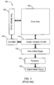
- CMOS image sensor device 100 includes a pixel array 105 with a plurality of pixels arranged in a two-dimensional pattern of row and column lines.
- the CMOS image sensor device 100 is operated by a controller 110, which controls the selection of pixels from the pixel array 105 to be read out. All pixels in a row are turned out simultaneously and readout in parallel by a plurality of column readout circuits 115.
- the pixels in a row line are selected and activated by row selector circuit 120 in response to control signals from controller 110.
- the row selector circuit 120 applies a driving voltage to the selected row line to activate the pixels in the selected line.
- the pixels in the selected line are then read out by the column readout circuits 115 in response to control signals from controller 110.
- Each column line is connected to a column readout circuit.
- the column readout circuits are, in turn, connected to pixel output stage 125.
- the pixel output stage 125 takes the electrical charges readout by the column readout circuits 115 and converts them into digital image samples. The samples are then processed at processor 130 for generating the digital image output 135.
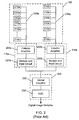
- Column readout circuits 115 connected to an output stage 125 include column amplifiers 205a-b for amplifying the electrical charges readout from pixels 210a in column line 215a and the electrical charges readout from pixels 210b in column line 215b, respectively.
- Column readout circuits 115a-b also include sample and hold circuits 220a-b for reading out the amplified charges.
- the column lines 215a-b also referred to as "bit lines,” are the lines to which all of the pixels of a given column are connected and from which the electrical charges from each pixel are read.
- the electrical charges are input into pixel output stage 125, which includes second stage or global amplifier 225 for further amplification of the electrical charges and ADC 230 for converting the electrical charges into digital image samples.
- a typical pixel in pixel array 105 may employ a photodetector followed by a four-transistor ("4T") configuration as shown in FIG. 3 .
- Pixel 300 includes a photodetector 305 followed by a transfer transistor 310, a reset transistor 315, a source follower transistor 320, and a row select transistor 325.
- the photodetector 305 converts the incident light into an electrical charge.
- the electrical charge is received by a floating diffusion region 330 through the transfer transistor 310 when the transfer transistor 310 is activated by the transfer gate control signal "TX.”
- the reset transistor 315 is connected between the floating diffusion region 330 and a supply voltage line 335.
- a reset control signal "RST” is used to activate the reset transistor 310 for resetting the floating diffusion region 330 to the supply voltage V cc at supply voltage line 335 prior to transferring the electrical charge from photodetector 305.
- the source follower transistor 320 is connected to the floating diffusion region 330 between the supply voltage line 335 and the row select transistor 325.
- the source follower transistor 320 converts the electrical charge stored at the floating diffusion region 330 into an output voltage "V out .”
- the row select transistor 325 is controlled by a row select signal "RS" for selectively connecting the source follower transistor 320 and its output voltage V out into a column line 340 of a pixel array.
- the 4T configuration shown at FIG. 3 was introduced to improve the overall image quality produced by CMOS image sensor devices.
- Image quality at a CMOS image sensor device depends on a host of factors, such as, for example, the noise sources introduced by the circuitry in the sensor and the dynamic range achievable with such circuitry.
- the noise sources include fixed pattern noise ("FPN") and read noise introduced by the column readout circuits, reset noise introduced by the reset transistor, photon shot noise introduced by the photodetector, and other noise sources such as dark current noise and thermal noise.
- the FPN can be significantly reduced or eliminated with the use of specialized column amplifiers or by performing flat-field correction.
- United States Patent No. 6,128,039 describes a column amplifier using a switching capacitor amplifier for high FPN reduction.
- the reset noise can also be eliminated with the use of a technique called Correlated Double Sampling ("CDS") at the sample and hold circuit stage of the column readout circuit.
- CDS samples the voltage output at the column line twice, during reset of the reset transistor and during the transfer of the output voltage at the source follower transistor. The samples are subtracted from each other thereby cancelling the reset noise.
- Other forms of noise such as the photon shot noise, the dark current noise, and the thermal noise are more difficult to cancel.
- the dynamic range is defmed as the ratio of the largest detectable luminance signal to the smallest.
- a high dynamic range is desirable in low-light conditions and for capturing images with large variations in luminance, that is, for capturing the wide range of luminance levels found in most real-world scenes.
- the dynamic range of a sensor is increased, the ability to simultaneously record the dimmest and brightest intensities in an image is improved.
- the dynamic range of an image sensor is usually expressed in gray levels, decibels or bits.
- Image sensors having higher signal-to-noise ratios produce higher dynamic range values (more decibels or bits).
- image sensors having ADCs of higher bit depths also produce higher dynamic range values.
- a 12-bit ADC corresponds to slightly over 4,000 gray levels or 72 dBs, while a 10-bit ADC can resolve only 1,000 gray levels for a 60 dB dynamic range.
- CMOS image sensor devices employing high bit depth ADCs, such as 14-bit ADCs, are known, but these devices tend to be costly, require more complex column readout circuits, and consume a considerably higher amount of power and semiconductor die area as compared to their CCD counterparts.
- the present invention provides an image sensor according to Claim 1.
- an image sensor apparatus has an image sensor for generating a first and a second set of digital image samples at a first bit depth, each set of digital image samples generated by a different column readout circuit path.
- a processor combines the first and the second set of digital image samples to generate a digital image at a second bit depth, the second bit depth higher than the first bit depth.
- An embodiment of the invention includes an image sensor apparatus for emulating a dynamic range achievable with a first bit depth analog-to-digital converter.
- the image sensor apparatus includes an array of pixels arranged in a plurality of row lines and column lines.
- a plurality of first and second column readout circuits are connected in parallel to the plurality of column lines, each first column readout circuit connected to a first output stage and each second column readout circuit connected to a second output stage, the first and second output stages generating digital image samples at a second bit depth.
- a processor is connected to the first and second output stages to receive the digital image samples and generate a digital image output of the first bit depth from the digital image samples.
- Another embodiment of the invention includes a method for providing high dynamic range digital images with a CMOS image sensor. Electrical charges are generated from incident light with an array of pixels arranged in a plurality of row lines and column lines. The electrical charges are read from the array of pixels with a plurality of first and second column readout circuits connected in parallel to the plurality of column lines, the first and second column readout circuits having different amplification responses. The electrical charges are converted into digital image samples of a first bit depth with a first and a second output stages, the first output stage connected to the plurality of first column readout circuits and the second output stage connected to the plurality of second column readout circuits. The digital image samples are processed to generate a digital image output at a second bit depth.
- a further embodiment of the invention includes an image sensor apparatus for generating a digital image output and including an image sensor for generating digital image samples at a first depth with a first and second column readout circuit paths of different amplification responses, the first bit depth smaller than a second bit depth of the digital image output.
- FIG. 1 illustrates a prior art CMOS image sensor apparatus
- FIG. 2 illustrates a prior art column readout circuit and an output stage for use with the CMOS image sensor apparatus of FIG. 1 ;
- FIG. 3 illustrates a prior art pixel for use with the CMOS image sensor apparatus of FIG. 1 ;
- FIG. 4 illustrates a CMOS image sensor apparatus constructed in according to an embodiment of the invention
- FIG. 5 illustrates a more detailed view of the CMOS image sensor apparatus of FIG. 4 ;
- FIG. 6 illustrates a further detailed view of the CMOS image sensor apparatus of FIG. 4 ;
- FIG. 7 illustrates a sample and hold circuit for use with the CMOS image sensor apparatus of FIG. 4 ;
- FIG. 8 illustrates a view of a CMOS image sensor apparatus including the sample and hold circuit of FIG. 7 and constructed according to an embodiment of the invention.
- an image sensor apparatus for generating high dynamic range digital images.
- an image sensor may be a device or circuitry having an array of pixels for capturing and processing an optical image into electronic signals.
- the electronic signals may be typically read by readout circuits, converted into digital image samples by output stages following the readout circuits and processed by an image signal processor ("ISP") or other device or circuitry capable of processing digital image samples into digital images or video.
- ISP image signal processor
- the readout circuits may be any circuit capable of reading out electrical charges accumulated by pixels in an image sensor.
- the output stages following the readout circuits may include analog-to-digital converters ("ADCs") for converting the electrical charges read by the readout circuitry into digital image samples.
- ADCs analog-to-digital converters
- the ISP in turn may include various executable routines for processing the digital image samples to generate a digital image output.
- Image sensor apparatus 400 has pixel array 405 composed of a plurality of pixels arranged in a two-dimensional pattern of row lines and column lines. Each pixel in pixel array 405 receives incident light and converts it into electrical charges corresponding to image information captured by the incident light.
- pixels in pixel array 405 may be pixels having the four transistor configuration shown in FIG. 3 . It is also appreciated that each pixel may include a row select "RS" control signal input indicative of a row selected for readout at any given time.
- the electrical charges accumulated in each pixel are read out in parallel one row at a time.
- all the pixels of a given row are read out in parallel by a plurality of column readout circuits, with each column readout circuit reading out the electrical charges accumulated in the pixels of a given column line.
- first and second column readout circuits 420-425 include a sample and hold circuit for converting the electrical charges into a set of analog samples.
- the sample and hold circuit may be connected to one or more control signals indicative of a column selected for readout at any given time.
- the control signals may be, for example, generated by a controller (not shown) in CMOS image sensor apparatus 400.
- each column line in pixel array 405 is connected to a set of first and a second column readout circuits equivalent to (i.e., having the same circuit components as) first and second column readout circuits 420-425 connected to column line 410.
- First and second column readout circuits 420-425 are respectively connected to a first output stage 430 and to a second output stage 435.
- First column readout circuit 420 and first output stage 430 form first readout circuit path 445.
- second column readout circuit 425 and second output stage 435 form second readout circuit path 450.
- First and second output stages 430-435 convert the analog image samples generated by first and second column readout circuits 420-425 into a set of digital image samples.
- First output stage 430 converts the analog image samples generated by first column readout circuit 420 into a first set of digital image samples and second output stage 435 converts the analog image samples generated by second column readout circuit 425 into a second set of digital image samples.
- output stages 430-435 also amplify the analog image samples generated by first and second column readout circuits 420-425 prior to analog-to-digital conversion. It is appreciated that a single first output stage 430 and a single second output stage 435 are connected to all the column readout circuits used in CMOS image sensor apparatus 400 for reading out electrical charges accumulated in the pixels of pixel array 405. It is also appreciated that first and second output stages 430-435 each receive a set of analog image samples corresponding to a single pixel at a time in response to control signals indicative of a row and a column selected for readout, as described in more detail herein below.
- first and second output stages 430-435 convert the analog image samples generated by first and second column readout circuits 420-425 into the first and second set of digital image samples using ADCs of a first bit depth, for example, using 10-bit ADCs.
- the first and second set of digital image samples generated by first and second output stages 430-435 are processed by processor 440 to generate a digital image output. It is appreciated that the first and second set of digital image samples correspond to the electrical charges accumulated in a single pixel. As such, the first and second set of digital image samples may be equivalent and represent redundant information.
- Processor 440 may include an ISP or a DSP for processing digital image samples into a digital image output.
- processor 440 is a processor having a second bit depth, for example, a 14-bit ISP.
- the second bit depth may be at least equal to or higher than the first bit depth.
- Processor 440 may include routines for combining digital image samples of a first bit depth to generate a digital image output of a second bit depth. For example, processor 440 may include a routine for averaging the first set of digital image samples generated by output stage 430 with the second set of digital image samples generated by output stage 435. Other routines may be used to combine the first and second set of digital image samples to form the digital image output.
- CMOS image sensor apparatus 400 uses two redundant sets of digital image samples at a first bit depth to generate a digital image output at a second bit depth to improve the dynamic range of the CMOS image sensor apparatus 400 with the use of simpler and less expensive circuitry than traditionally required for a digital image output of a second bit depth.
- a digital image output of a second bit depth may be achieved without the use of ADCs having the second bit depth and their associated more complex and costly column readout circuits.
- a 14-bit dynamic range may be achieved with the use of two 10-bit ADCs, one in first output stage 430 and another in second output stage 435. It is appreciated that the use of two 10-bit ADCs provide a significant savings over the use of a single 14-bit ADC without the need to employ complex calibration procedures generally required for higher bit depths ADCs.
- CMOS image sensor apparatus 400 to emulate the high dynamic ranges achievable with high bit depth ADCs by using lower bit depth ADCs. It is appreciated that current ADCs for use with CMOS image sensors may be considered to have high bit depths if they have at least a 14-bit depth. It is also appreciated that ADCs and processors of other bit depths, e.g., higher than 14 bits, may be used without deviating from the principles and embodiments of the invention.
- First column readout circuit 420 includes a column amplifier 500 for amplifying the electrical charges accumulated in each pixel 415 of column line 410 and a sample and hold circuit 505 for converting the amplified electrical charges into a first set of analog image samples.
- Second column readout circuit 425 does not include a column amplifier and reads out the electrical charges accumulated in each pixel 415 of column line 410 directly into a sample and hold circuit 510. It is appreciated that the sample and hold circuit 505 in first column readout circuit 420 and the sample and hold circuit 510 in second column readout circuit 425 may be equivalent, that is, containing the same circuit components.
- first column readout circuit 420 may provide two signal paths in CMOS image sensor apparatus 400 having different amplification responses.
- First column readout circuit 420 together with output stage 430 may be used to provide a first column readout circuit path 445 and second column readout circuit 425 together with output stage 435 may be used to provide a second column readout circuit path 450.
- First column readout circuit path 445 may be a "bright” signal path as column amplifier 500 amplifies the electrical charges accumulated in pixels 415 of column line 410 to capture higher and brighter luminance values and achieve a higher dynamic range.
- Second column readout circuit path 450 without a column amplifier, may be a "dark" signal path to capture the lower and darker luminance values and also contribute to the higher dynamic range of CMOS image sensor apparatus 400.
- second column readout circuit 425 may also include a column amplifier to further improve the dynamic range of CMOS image sensor apparatus 400. Further, it is appreciated that column amplifier 500 in column readout circuit 420 may be a column amplifier specifically designed to achieve a higher dynamic range.
- first and second column readout circuit paths 445-450 may be designed to provide a given amplification response to achieve a desired dynamic range.
- first column readout circuit path 445 may be designed with an amplification response to capture as many bright luminance values as desired.
- second column readout circuit 450 may be designed with an amplification response to capture as many dark luminance values as desired.
- the use of two column readout circuit paths having a bit depth of "n" bits with one column readout circuit path providing an amplification response of a gain of "2 K " results in a "n + k" dynamic range.
- CMOS image sensor apparatus 400 may be designed with a bit depth and column readout circuit paths having amplification responses as desired to achieve a given dynamic range.
- First and second output stages 430-435 include a global amplifier to provide further amplification of the electrical charges accumulated in pixels 415 of column line 410 and also improve the dynamic range of CMOS image sensor apparatus 400.
- First output stage 430 includes global amplifier 510 and second output stage 435 includes global amplifier 520.
- the global amplifier 510 and the global amplifier 520 are in turn connected to ADCs 515 and 525, respectively.
- ADCs 515 and 525 may be ADCs having a first bit depth.
- global amplifier 510 and global amplifier 520 may be equivalent, i.e., containing the same circuit components. It is also appreciated that ADCs 515 and 525 may be equivalent without deviating from the principles and embodiments of the invention.
- FIG. 6 A further detailed view of the CMOS image sensor apparatus 400 shown in FIG. 5 is illustrated in FIG. 6 .
- Pixel array 405 in CMOS image sensor apparatus 400 is shown with two column lines, column line 410 and column line 600.
- Each column line of pixel array 405 has a set of first and second column readout circuits connected to it.
- Column line 410 is connected to first column readout circuit 420 and second column readout circuit 425.
- Column line 600 is in turn connected to first column readout circuit 610 and second column readout circuit 615.
- first column readout circuit 610 also includes a column amplifier 620 and a sample and hold circuit 625. And similar to second column readout circuit 425, second column readout circuit 615 also includes a sample and hold circuit 630 directly connected to a column line. It is appreciated that column amplifiers 500 and 620 may be equivalent. It is also appreciated that sample and hold circuits 505, 510, 625, and 630 may also be equivalent.
- First column readout circuits 420 and 610 are both selectively connected to first output stage 430. Conversely, second column readout circuits 425 and 615 are both selectively connected to second output stage 425. Control signals input to sample and hold circuits 505, 510, 625, and 630 indicate the column of pixel array 405 selected for processed at any given time by first and second output stages 430-435.
- Sample and hold circuit 700 include a first set of transistors 705 and 710 and a second set of transistors 715 and 720.
- the first set of transistors 705 and 710 are driven by a control signal indicative of a horizontal blanking interval used in the horizontal (i.e., row) scanning of pixel array 405 ("HBLK").
- the second set of transistors 715-720 are driven by a control signal indicative of a column selected for readout ("CS").
- a capacitor “C BLK” 725 holds the electrical charges accumulated in a pixel of pixel array 400 and read into transistor 705.
- a capacitor “C SIG” holds the electrical charges accumulated in a pixel array 400 and read into transistor 715. The electrical charges held by capacitors 730 are then released to transistors 715-720 for generating a set of analog image samples corresponding to the electrical charges.
- capacitors 725-730 are required to have a size to support only the first bit depth used by the ADCs in the output stages 430-435 following the first and second column readout circuits 420-425. Capacitors 725-730 may be smaller than the capacitors used to support the second bit depth of the processor 440.
- CMOS image sensor apparatus 400 is able to provide a higher dynamic range of the second bit depth by using much smaller capacitors than would traditionally be required for capacitors sized to support the second bit depth. This provides further savings in circuitry manufacturing and complexity costs while achieving a higher dynamic range.
- sample and hold circuit 700 is a correlated double sampler.
- the first set of analog image samples acquired at transistor 715 corresponds to image samples readout during reset of the reset transistor in each pixel of pixel array 705.
- the second set of analog image samples acquired at transistor 720 corresponds to image samples readout after the reset period.
- the first and second set of analog image samples may then be subtracted from each other at the following output stage to eliminate the reset noise in CMOS image sensor apparatus 400.
- CMOS image sensor apparatus 400 is shown with column line 800 connected to pixels 805.
- First column readout circuit 420 includes column amplifier 810 and sample and hold circuit 815 designed according to the exemplary embodiment shown in FIG. 7 .
- Second column readout circuit 415 includes sample and hold circuit 820 also designed according to the exemplary embodiment shown in FIG. 7 .
- First output stage 430 connected to first column readout circuit 420 includes global amplifier 825 and ADC of a first bit depth 830.
- Second output stage 435 connected to second column readout circuit 425 includes global amplifier 835 and ADC of a first bit depth 840.
- the first and second output stages 430-435 are connected to processor 440 for generating a digital image output.
- sample and hold circuits 815-820 may be equivalent. It is also appreciated that global amplifiers 825 and 835 may also be equivalent. In an exemplary embodiment, sample and hold circuits 815-820 may be correlated double samplers and global amplifiers 825 and 835 may be differential amplifiers to subtract the first and second analog image sample sets generated by the correlated double samplers. Further, it is appreciated that ADCs 830 and 840 may also be equivalent.
- first and second output stages are connected to a plurality of first and second column readout circuits, with each first and second column readout circuits connected to a given column line of pixel array 405. It is also appreciated that the "RS" (row select) control signal in each pixel of pixel array 405 and the "CS" (column select) control signal in each sample and hold circuit of the column readout circuits indicate to output stages 430-435 which pixel in a given row and column is to be read out at any given time.
- the CMOS image sensor apparatus 400 generates a digital image output having a higher dynamic range while using simpler and less costly circuit components.
- the CMOS image sensor apparatus 400 may achieve a 14-bit dynamic range while using only 10-bit ADCs and sample and hold circuits having capacitors sized to support 10-bit ADCs. This enables the dynamic range gap currently in place between CMOS and CCD image sensors to be reduced significantly, as the CMOS image sensor apparatus 400 provides digital images of high dynamic ranges with design and manufacturing costs similar to or better than those of CCD image sensors counterparts.
Applications Claiming Priority (1)
| Application Number | Priority Date | Filing Date | Title |
|---|---|---|---|
| US11/856,014 US7995124B2 (en) | 2007-09-14 | 2007-09-14 | Image sensor apparatus and method for improved dynamic range with multiple readout circuit paths |
Publications (3)
| Publication Number | Publication Date |
|---|---|
| EP2037668A2 true EP2037668A2 (de) | 2009-03-18 |
| EP2037668A3 EP2037668A3 (de) | 2012-04-18 |
| EP2037668B1 EP2037668B1 (de) | 2019-01-23 |
Family
ID=40119663
Family Applications (1)
| Application Number | Title | Priority Date | Filing Date |
|---|---|---|---|
| EP08252987.6A Active EP2037668B1 (de) | 2007-09-14 | 2008-09-10 | Bildsensorvorrichtung und Verfahren für den verbesserten dynamischen Bereich mit mehreren Leseschaltungspfaden |
Country Status (4)
| Country | Link |
|---|---|
| US (1) | US7995124B2 (de) |
| EP (1) | EP2037668B1 (de) |
| CN (1) | CN101534376B (de) |
| TW (1) | TWI415454B (de) |
Cited By (2)
| Publication number | Priority date | Publication date | Assignee | Title |
|---|---|---|---|---|
| DE102009019034A1 (de) * | 2009-04-27 | 2010-10-28 | Arnold & Richter Cine Technik Gmbh & Co. Betriebs Kg | Bildsensor |
| EP2549743A3 (de) * | 2011-07-19 | 2014-03-12 | Canon Kabushiki Kaisha | Abbildungsvorrichtung |
Families Citing this family (29)
| Publication number | Priority date | Publication date | Assignee | Title |
|---|---|---|---|---|
| JP5212022B2 (ja) * | 2008-10-30 | 2013-06-19 | ソニー株式会社 | 固体撮像装置、撮像装置、画素駆動電圧適正化装置、画素駆動電圧適正化方法 |
| US7950286B2 (en) * | 2008-12-19 | 2011-05-31 | Honeywell International Inc. | Multi-range pressure sensor apparatus and method utilizing a single sense die and multiple signal paths |
| US10330513B2 (en) * | 2009-05-27 | 2019-06-25 | Honeywell International Inc. | Multi-dynamic-range sensor |
| JP5219962B2 (ja) * | 2009-08-13 | 2013-06-26 | キヤノン株式会社 | 固体撮像素子、その駆動方法、及び撮像システム |
| CN102170534B (zh) * | 2010-02-25 | 2013-08-28 | 英属开曼群岛商恒景科技股份有限公司 | 应用于影像传感器的处理器以及影像系统 |
| US8656772B2 (en) | 2010-03-22 | 2014-02-25 | Honeywell International Inc. | Flow sensor with pressure output signal |
| US8248490B2 (en) * | 2010-04-21 | 2012-08-21 | Omnivision Technologies, Inc. | Imaging sensor having reduced column fixed pattern noise |
| US8730364B2 (en) * | 2010-11-09 | 2014-05-20 | Omnivision Technologies, Inc. | Image sensor with pipelined column analog-to-digital converters |
| DE102010051986B4 (de) * | 2010-11-19 | 2024-02-01 | Arnold & Richter Cine Technik Gmbh & Co. Betriebs Kg | Bildsensor |
| US8643750B2 (en) | 2010-12-22 | 2014-02-04 | Omnivision Technologies, Inc. | Reducing noise in image sensors by concurrently reading reset and image signal levels from active and reference pixels |
| US8695417B2 (en) | 2011-01-31 | 2014-04-15 | Honeywell International Inc. | Flow sensor with enhanced flow range capability |
| US9077910B2 (en) | 2011-04-06 | 2015-07-07 | Dolby Laboratories Licensing Corporation | Multi-field CCD capture for HDR imaging |
| US8446220B2 (en) | 2011-05-09 | 2013-05-21 | Honeywell International Inc. | Method and apparatus for increasing the effective resolution of a sensor |
| CN102891150A (zh) * | 2011-07-22 | 2013-01-23 | 中国科学院微电子研究所 | 紫外探测器的像素结构、紫外探测器系统及其制造方法 |
| US8770034B2 (en) | 2011-09-06 | 2014-07-08 | Honeywell International Inc. | Packaged sensor with multiple sensors elements |
| US9052217B2 (en) | 2012-11-09 | 2015-06-09 | Honeywell International Inc. | Variable scale sensor |
| JP6261883B2 (ja) * | 2013-06-03 | 2018-01-17 | 浜松ホトニクス株式会社 | 光観察装置、それに用いる撮像装置、及び光観察方法 |
| JP6175355B2 (ja) * | 2013-11-07 | 2017-08-02 | ルネサスエレクトロニクス株式会社 | 固体撮像素子 |
| WO2015120328A1 (en) * | 2014-02-07 | 2015-08-13 | Rambus Inc. | Feedthrough-compensated image sensor |
| KR101629825B1 (ko) * | 2014-12-04 | 2016-06-22 | 현대모비스 주식회사 | Hdr 기능을 이용한 차량용 디스플레이 장치 및 방법 |
| US9380234B1 (en) | 2015-05-01 | 2016-06-28 | Omnivision Technologies, Inc. | Reduced random telegraph signal noise CMOS image sensor and associated method |
| KR102440362B1 (ko) * | 2015-09-25 | 2022-09-05 | 삼성전자주식회사 | 이미지 센서, 적층형 이미지 센서, 이미지 처리 장치 및 이미지 센서 칩 패키지의 제조 방법 |
| CN106682311B (zh) * | 2016-12-27 | 2020-11-06 | 上海集成电路研发中心有限公司 | 一种图像传感器像素单元晶体管的建模方法 |
| JP6918517B2 (ja) * | 2017-02-21 | 2021-08-11 | キヤノン株式会社 | 撮像素子及びその制御方法、及び撮像装置 |
| US10255968B2 (en) * | 2017-07-24 | 2019-04-09 | Omnivision Technologies, Inc. | DRAM core architecture with wide I/Os |
| US20210251574A1 (en) * | 2018-08-24 | 2021-08-19 | The Trustees Of Dartmouth College | Microcontroller for recording and storing physiological data |
| US10834351B2 (en) * | 2018-11-26 | 2020-11-10 | Omnivision Technologies, Inc. | Bitline settling speed enhancement |
| WO2021020009A1 (ja) * | 2019-07-26 | 2021-02-04 | 富士フイルム株式会社 | 撮像装置、撮像素子、撮像装置の作動方法、撮像素子の作動方法、及びプログラム |
| DE102020127129A1 (de) | 2020-10-15 | 2022-04-21 | Arnold & Richter Cine Technik Gmbh & Co. Betriebs Kg | Bildwandler |
Citations (4)
| Publication number | Priority date | Publication date | Assignee | Title |
|---|---|---|---|---|
| EP0379588A1 (de) | 1988-06-10 | 1990-08-01 | Kubota Corporation | Vorrichtung und verfahren zum mahlen und pulverisieren |
| US6128039A (en) | 1999-01-11 | 2000-10-03 | Omnivision Technologies, Inc. | Column amplifier for high fixed pattern noise reduction |
| JP2002232291A (ja) | 2001-02-02 | 2002-08-16 | Riniaseru Design:Kk | アナログ−デジタル変換器及びこれを用いたイメージセンサ |
| US20070046795A1 (en) | 2004-06-07 | 2007-03-01 | Canon Kabushiki Kaisha | Image pickup device and image pickup system |
Family Cites Families (25)
| Publication number | Priority date | Publication date | Assignee | Title |
|---|---|---|---|---|
| JPS56125115A (en) * | 1980-03-06 | 1981-10-01 | Mitsubishi Electric Corp | Analog and digital converter |
| US4733217A (en) * | 1986-05-08 | 1988-03-22 | Rca Corporation | Subranging analog to digital converter |
| CA1340064C (en) * | 1988-06-08 | 1998-09-29 | Mitsuo Kakuishi | Signal processing apparatus with dual parallel a/d and d/a converters |
| JP3153271B2 (ja) * | 1991-07-05 | 2001-04-03 | 株式会社日立製作所 | Ad変換器 |
| JPH0595287A (ja) * | 1991-10-01 | 1993-04-16 | Mitsubishi Electric Corp | 減算回路および減算回路を備えるa/dコンバータ |
| US6456326B2 (en) | 1994-01-28 | 2002-09-24 | California Institute Of Technology | Single chip camera device having double sampling operation |
| US5790191A (en) | 1996-03-07 | 1998-08-04 | Omnivision Technologies, Inc. | Method and apparatus for preamplification in a MOS imaging array |
| CN1252987C (zh) * | 2001-08-17 | 2006-04-19 | 微米技术有限公司 | 用于提高固态成像仪的读取速度的装置和方法 |
| JP4434530B2 (ja) * | 2001-09-17 | 2010-03-17 | ソニー株式会社 | 固体撮像装置 |
| US7382407B2 (en) * | 2002-08-29 | 2008-06-03 | Micron Technology, Inc. | High intrascene dynamic range NTSC and PAL imager |
| KR100484278B1 (ko) * | 2003-02-07 | 2005-04-20 | (주)실리콘화일 | 넓은 동작 범위를 갖는 광 화상 수신용 디바이스 |
| US6953923B2 (en) | 2003-02-18 | 2005-10-11 | Omnivision Technologies, Inc. | CMOS image sensor having reduced numbers of column readout circuits |
| US7078746B2 (en) | 2003-07-15 | 2006-07-18 | Micron Technology, Inc. | Image sensor with floating diffusion gate capacitor |
| JP4161855B2 (ja) * | 2003-09-10 | 2008-10-08 | ソニー株式会社 | 固体撮像装置、駆動制御方法及び駆動制御装置 |
| US7446812B2 (en) * | 2004-01-13 | 2008-11-04 | Micron Technology, Inc. | Wide dynamic range operations for imaging |
| US7196304B2 (en) | 2004-01-29 | 2007-03-27 | Micron Technology, Inc. | Row driver for selectively supplying operating power to imager pixel |
| US7332703B2 (en) | 2004-03-22 | 2008-02-19 | Micron Technology, Inc. | Imaging structure including a pixel with multiple signal readout circuits and methods of operation for imaging structure |
| JP4315032B2 (ja) * | 2004-03-22 | 2009-08-19 | ソニー株式会社 | 固体撮像装置および固体撮像装置の駆動方法 |
| US7091531B2 (en) | 2004-04-07 | 2006-08-15 | Micron Technology, Inc. | High dynamic range pixel amplifier |
| US6999019B2 (en) * | 2004-04-08 | 2006-02-14 | The Boeing Company | Subranging analog-to-digital converter with integrating sample-and-hold |
| JP3976754B2 (ja) | 2004-07-13 | 2007-09-19 | マイクロン テクノロジー,インコーポレイテッド | 選択読取りによる広ダイナミックレンジ撮像デバイス |
| US7259413B2 (en) | 2004-09-28 | 2007-08-21 | Micron Technology, Inc. | High dynamic range image sensor |
| US7345330B2 (en) * | 2004-12-09 | 2008-03-18 | Omnivision Technologies, Inc. | Local interconnect structure and method for a CMOS image sensor |
| JP4802767B2 (ja) * | 2006-03-06 | 2011-10-26 | ソニー株式会社 | アナログ−デジタル変換装置と、それを用いた固体撮像装置とその駆動方法 |
| US7247831B1 (en) * | 2006-07-25 | 2007-07-24 | Micron Technology, Inc. | Reduction in size of column sample and hold circuitry in a CMOS imager |
-
2007
- 2007-09-14 US US11/856,014 patent/US7995124B2/en active Active
-
2008
- 2008-08-22 TW TW097132190A patent/TWI415454B/zh active
- 2008-09-10 EP EP08252987.6A patent/EP2037668B1/de active Active
- 2008-09-16 CN CN200810149014.4A patent/CN101534376B/zh active Active
Patent Citations (4)
| Publication number | Priority date | Publication date | Assignee | Title |
|---|---|---|---|---|
| EP0379588A1 (de) | 1988-06-10 | 1990-08-01 | Kubota Corporation | Vorrichtung und verfahren zum mahlen und pulverisieren |
| US6128039A (en) | 1999-01-11 | 2000-10-03 | Omnivision Technologies, Inc. | Column amplifier for high fixed pattern noise reduction |
| JP2002232291A (ja) | 2001-02-02 | 2002-08-16 | Riniaseru Design:Kk | アナログ−デジタル変換器及びこれを用いたイメージセンサ |
| US20070046795A1 (en) | 2004-06-07 | 2007-03-01 | Canon Kabushiki Kaisha | Image pickup device and image pickup system |
Cited By (4)
| Publication number | Priority date | Publication date | Assignee | Title |
|---|---|---|---|---|
| DE102009019034A1 (de) * | 2009-04-27 | 2010-10-28 | Arnold & Richter Cine Technik Gmbh & Co. Betriebs Kg | Bildsensor |
| US8344307B2 (en) | 2009-04-27 | 2013-01-01 | Arnold & Richter Cine Technik Gmbh & Co. Betriebs Kg | Image sensor |
| EP2549743A3 (de) * | 2011-07-19 | 2014-03-12 | Canon Kabushiki Kaisha | Abbildungsvorrichtung |
| US9148590B2 (en) | 2011-07-19 | 2015-09-29 | Canon Kabushiki Kaisha | Imaging apparatus with reference signals having different rate of change first and second pixels having same color |
Also Published As
| Publication number | Publication date |
|---|---|
| TWI415454B (zh) | 2013-11-11 |
| US20090073274A1 (en) | 2009-03-19 |
| TW200915863A (en) | 2009-04-01 |
| EP2037668B1 (de) | 2019-01-23 |
| CN101534376B (zh) | 2013-09-18 |
| EP2037668A3 (de) | 2012-04-18 |
| CN101534376A (zh) | 2009-09-16 |
| US7995124B2 (en) | 2011-08-09 |
Similar Documents
| Publication | Publication Date | Title |
|---|---|---|
| US7995124B2 (en) | Image sensor apparatus and method for improved dynamic range with multiple readout circuit paths | |
| US20200259986A1 (en) | Method and apparatus providing pixel array having automatic light control pixels and image capture pixels | |
| US7667176B2 (en) | Readout technique for increasing or maintaining dynamic range in image sensors | |
| JP4609428B2 (ja) | 固体撮像装置、固体撮像装置の駆動方法および撮像装置 | |
| EP1788797B1 (de) | Festkörper-Bildaufnahmevorrichtung | |
| US8130302B2 (en) | Methods and apparatus providing selective binning of pixel circuits | |
| JP4691930B2 (ja) | 物理情報取得方法および物理情報取得装置、並びに物理量分布検知の半導体装置、プログラム、および撮像モジュール | |
| US20100321532A1 (en) | Solid-state imaging device, imaging system, and method of driving solid-state imaging device | |
| US20070045677A1 (en) | Method and apparatus for calibrating parallel readout paths in imagers | |
| EP2448254B1 (de) | Festkörperbildaufnahmevorrichtung | |
| US20060187329A1 (en) | Clamped capacitor readout noise rejection circuit for imagers | |
| US8085324B2 (en) | Solid-state imaging apparatus | |
| JP5019705B2 (ja) | 固体撮像装置及び固体撮像装置の駆動方法 | |
| WO2006113271A1 (en) | Multi-point correlated sampling for image sensors | |
| JP2008263546A (ja) | 固体撮像装置、固体撮像装置の駆動方法、及びこれを用いた撮像システム | |
| KR101939402B1 (ko) | 고체 촬상 소자 및 구동 방법, 및 전자 기기 | |
| US8149308B2 (en) | Solid-state image pickup device | |
| US20050146617A1 (en) | Imaging apparatus for processing noise signal and photoelectric conversion signal | |
| JP5487845B2 (ja) | 撮像素子、駆動制御方法、並びにプログラム | |
| JP5966357B2 (ja) | 撮像素子および撮像装置 | |
| JP4677228B2 (ja) | 撮像装置 | |
| JP2006197229A (ja) | 撮像装置およびカメラ | |
| US20240022836A1 (en) | Solid-state imaging device, method for driving solid-state imaging device, and electronic apparatus | |
| JP2012070056A (ja) | 撮像装置 |
Legal Events
| Date | Code | Title | Description |
|---|---|---|---|
| PUAI | Public reference made under article 153(3) epc to a published international application that has entered the european phase |
Free format text: ORIGINAL CODE: 0009012 |
|
| AK | Designated contracting states |
Kind code of ref document: A2 Designated state(s): AT BE BG CH CY CZ DE DK EE ES FI FR GB GR HR HU IE IS IT LI LT LU LV MC MT NL NO PL PT RO SE SI SK TR |
|
| AX | Request for extension of the european patent |
Extension state: AL BA MK RS |
|
| PUAL | Search report despatched |
Free format text: ORIGINAL CODE: 0009013 |
|
| AK | Designated contracting states |
Kind code of ref document: A3 Designated state(s): AT BE BG CH CY CZ DE DK EE ES FI FR GB GR HR HU IE IS IT LI LT LU LV MC MT NL NO PL PT RO SE SI SK TR |
|
| AX | Request for extension of the european patent |
Extension state: AL BA MK RS |
|
| 17P | Request for examination filed |
Effective date: 20120921 |
|
| AKX | Designation fees paid |
Designated state(s): AT BE BG CH CY CZ DE DK EE ES FI FR GB GR HR HU IE IS IT LI LT LU LV MC MT NL NO PL PT RO SE SI SK TR |
|
| REG | Reference to a national code |
Ref country code: DE Ref legal event code: R079 Ref document number: 602008058839 Country of ref document: DE Free format text: PREVIOUS MAIN CLASS: H04N0003150000 Ipc: H04N0005378000 |
|
| GRAP | Despatch of communication of intention to grant a patent |
Free format text: ORIGINAL CODE: EPIDOSNIGR1 |
|
| STAA | Information on the status of an ep patent application or granted ep patent |
Free format text: STATUS: GRANT OF PATENT IS INTENDED |
|
| RIC1 | Information provided on ipc code assigned before grant |
Ipc: H04N 5/355 20110101ALI20180827BHEP Ipc: H04N 5/378 20110101AFI20180827BHEP Ipc: H04N 5/235 20060101ALI20180827BHEP |
|
| INTG | Intention to grant announced |
Effective date: 20180917 |
|
| RAP1 | Party data changed (applicant data changed or rights of an application transferred) |
Owner name: OMNIVISION TECHNOLOGIES, INC. |
|
| GRAS | Grant fee paid |
Free format text: ORIGINAL CODE: EPIDOSNIGR3 |
|
| GRAA | (expected) grant |
Free format text: ORIGINAL CODE: 0009210 |
|
| STAA | Information on the status of an ep patent application or granted ep patent |
Free format text: STATUS: THE PATENT HAS BEEN GRANTED |
|
| AK | Designated contracting states |
Kind code of ref document: B1 Designated state(s): AT BE BG CH CY CZ DE DK EE ES FI FR GB GR HR HU IE IS IT LI LT LU LV MC MT NL NO PL PT RO SE SI SK TR |
|
| REG | Reference to a national code |
Ref country code: GB Ref legal event code: FG4D |
|
| REG | Reference to a national code |
Ref country code: CH Ref legal event code: EP |
|
| RIC2 | Information provided on ipc code assigned after grant |
Ipc: H04N 5/235 20060101ALI20180827BHEP Ipc: H04N 5/355 20110101ALI20180827BHEP Ipc: H04N 5/378 20110101AFI20180827BHEP |
|
| REG | Reference to a national code |
Ref country code: AT Ref legal event code: REF Ref document number: 1092390 Country of ref document: AT Kind code of ref document: T Effective date: 20190215 |
|
| REG | Reference to a national code |
Ref country code: IE Ref legal event code: FG4D |
|
| REG | Reference to a national code |
Ref country code: DE Ref legal event code: R096 Ref document number: 602008058839 Country of ref document: DE |
|
| REG | Reference to a national code |
Ref country code: NL Ref legal event code: MP Effective date: 20190123 |
|
| PG25 | Lapsed in a contracting state [announced via postgrant information from national office to epo] |
Ref country code: NL Free format text: LAPSE BECAUSE OF FAILURE TO SUBMIT A TRANSLATION OF THE DESCRIPTION OR TO PAY THE FEE WITHIN THE PRESCRIBED TIME-LIMIT Effective date: 20190123 |
|
| PG25 | Lapsed in a contracting state [announced via postgrant information from national office to epo] |
Ref country code: NO Free format text: LAPSE BECAUSE OF FAILURE TO SUBMIT A TRANSLATION OF THE DESCRIPTION OR TO PAY THE FEE WITHIN THE PRESCRIBED TIME-LIMIT Effective date: 20190423 Ref country code: FI Free format text: LAPSE BECAUSE OF FAILURE TO SUBMIT A TRANSLATION OF THE DESCRIPTION OR TO PAY THE FEE WITHIN THE PRESCRIBED TIME-LIMIT Effective date: 20190123 Ref country code: LT Free format text: LAPSE BECAUSE OF FAILURE TO SUBMIT A TRANSLATION OF THE DESCRIPTION OR TO PAY THE FEE WITHIN THE PRESCRIBED TIME-LIMIT Effective date: 20190123 Ref country code: PL Free format text: LAPSE BECAUSE OF FAILURE TO SUBMIT A TRANSLATION OF THE DESCRIPTION OR TO PAY THE FEE WITHIN THE PRESCRIBED TIME-LIMIT Effective date: 20190123 Ref country code: PT Free format text: LAPSE BECAUSE OF FAILURE TO SUBMIT A TRANSLATION OF THE DESCRIPTION OR TO PAY THE FEE WITHIN THE PRESCRIBED TIME-LIMIT Effective date: 20190523 Ref country code: ES Free format text: LAPSE BECAUSE OF FAILURE TO SUBMIT A TRANSLATION OF THE DESCRIPTION OR TO PAY THE FEE WITHIN THE PRESCRIBED TIME-LIMIT Effective date: 20190123 Ref country code: SE Free format text: LAPSE BECAUSE OF FAILURE TO SUBMIT A TRANSLATION OF THE DESCRIPTION OR TO PAY THE FEE WITHIN THE PRESCRIBED TIME-LIMIT Effective date: 20190123 |
|
| REG | Reference to a national code |
Ref country code: AT Ref legal event code: MK05 Ref document number: 1092390 Country of ref document: AT Kind code of ref document: T Effective date: 20190123 |
|
| PG25 | Lapsed in a contracting state [announced via postgrant information from national office to epo] |
Ref country code: LV Free format text: LAPSE BECAUSE OF FAILURE TO SUBMIT A TRANSLATION OF THE DESCRIPTION OR TO PAY THE FEE WITHIN THE PRESCRIBED TIME-LIMIT Effective date: 20190123 Ref country code: BG Free format text: LAPSE BECAUSE OF FAILURE TO SUBMIT A TRANSLATION OF THE DESCRIPTION OR TO PAY THE FEE WITHIN THE PRESCRIBED TIME-LIMIT Effective date: 20190423 Ref country code: GR Free format text: LAPSE BECAUSE OF FAILURE TO SUBMIT A TRANSLATION OF THE DESCRIPTION OR TO PAY THE FEE WITHIN THE PRESCRIBED TIME-LIMIT Effective date: 20190424 Ref country code: IS Free format text: LAPSE BECAUSE OF FAILURE TO SUBMIT A TRANSLATION OF THE DESCRIPTION OR TO PAY THE FEE WITHIN THE PRESCRIBED TIME-LIMIT Effective date: 20190523 Ref country code: HR Free format text: LAPSE BECAUSE OF FAILURE TO SUBMIT A TRANSLATION OF THE DESCRIPTION OR TO PAY THE FEE WITHIN THE PRESCRIBED TIME-LIMIT Effective date: 20190123 |
|
| REG | Reference to a national code |
Ref country code: DE Ref legal event code: R097 Ref document number: 602008058839 Country of ref document: DE |
|
| PG25 | Lapsed in a contracting state [announced via postgrant information from national office to epo] |
Ref country code: DK Free format text: LAPSE BECAUSE OF FAILURE TO SUBMIT A TRANSLATION OF THE DESCRIPTION OR TO PAY THE FEE WITHIN THE PRESCRIBED TIME-LIMIT Effective date: 20190123 Ref country code: EE Free format text: LAPSE BECAUSE OF FAILURE TO SUBMIT A TRANSLATION OF THE DESCRIPTION OR TO PAY THE FEE WITHIN THE PRESCRIBED TIME-LIMIT Effective date: 20190123 Ref country code: SK Free format text: LAPSE BECAUSE OF FAILURE TO SUBMIT A TRANSLATION OF THE DESCRIPTION OR TO PAY THE FEE WITHIN THE PRESCRIBED TIME-LIMIT Effective date: 20190123 Ref country code: CZ Free format text: LAPSE BECAUSE OF FAILURE TO SUBMIT A TRANSLATION OF THE DESCRIPTION OR TO PAY THE FEE WITHIN THE PRESCRIBED TIME-LIMIT Effective date: 20190123 Ref country code: IT Free format text: LAPSE BECAUSE OF FAILURE TO SUBMIT A TRANSLATION OF THE DESCRIPTION OR TO PAY THE FEE WITHIN THE PRESCRIBED TIME-LIMIT Effective date: 20190123 Ref country code: RO Free format text: LAPSE BECAUSE OF FAILURE TO SUBMIT A TRANSLATION OF THE DESCRIPTION OR TO PAY THE FEE WITHIN THE PRESCRIBED TIME-LIMIT Effective date: 20190123 |
|
| PLBE | No opposition filed within time limit |
Free format text: ORIGINAL CODE: 0009261 |
|
| STAA | Information on the status of an ep patent application or granted ep patent |
Free format text: STATUS: NO OPPOSITION FILED WITHIN TIME LIMIT |
|
| PG25 | Lapsed in a contracting state [announced via postgrant information from national office to epo] |
Ref country code: AT Free format text: LAPSE BECAUSE OF FAILURE TO SUBMIT A TRANSLATION OF THE DESCRIPTION OR TO PAY THE FEE WITHIN THE PRESCRIBED TIME-LIMIT Effective date: 20190123 |
|
| 26N | No opposition filed |
Effective date: 20191024 |
|
| PG25 | Lapsed in a contracting state [announced via postgrant information from national office to epo] |
Ref country code: SI Free format text: LAPSE BECAUSE OF FAILURE TO SUBMIT A TRANSLATION OF THE DESCRIPTION OR TO PAY THE FEE WITHIN THE PRESCRIBED TIME-LIMIT Effective date: 20190123 |
|
| PG25 | Lapsed in a contracting state [announced via postgrant information from national office to epo] |
Ref country code: TR Free format text: LAPSE BECAUSE OF FAILURE TO SUBMIT A TRANSLATION OF THE DESCRIPTION OR TO PAY THE FEE WITHIN THE PRESCRIBED TIME-LIMIT Effective date: 20190123 |
|
| PG25 | Lapsed in a contracting state [announced via postgrant information from national office to epo] |
Ref country code: MC Free format text: LAPSE BECAUSE OF FAILURE TO SUBMIT A TRANSLATION OF THE DESCRIPTION OR TO PAY THE FEE WITHIN THE PRESCRIBED TIME-LIMIT Effective date: 20190123 |
|
| PG25 | Lapsed in a contracting state [announced via postgrant information from national office to epo] |
Ref country code: LU Free format text: LAPSE BECAUSE OF NON-PAYMENT OF DUE FEES Effective date: 20190910 Ref country code: IE Free format text: LAPSE BECAUSE OF NON-PAYMENT OF DUE FEES Effective date: 20190910 |
|
| REG | Reference to a national code |
Ref country code: BE Ref legal event code: MM Effective date: 20190930 |
|
| PG25 | Lapsed in a contracting state [announced via postgrant information from national office to epo] |
Ref country code: BE Free format text: LAPSE BECAUSE OF NON-PAYMENT OF DUE FEES Effective date: 20190930 |
|
| PG25 | Lapsed in a contracting state [announced via postgrant information from national office to epo] |
Ref country code: CY Free format text: LAPSE BECAUSE OF FAILURE TO SUBMIT A TRANSLATION OF THE DESCRIPTION OR TO PAY THE FEE WITHIN THE PRESCRIBED TIME-LIMIT Effective date: 20190123 |
|
| PG25 | Lapsed in a contracting state [announced via postgrant information from national office to epo] |
Ref country code: MT Free format text: LAPSE BECAUSE OF FAILURE TO SUBMIT A TRANSLATION OF THE DESCRIPTION OR TO PAY THE FEE WITHIN THE PRESCRIBED TIME-LIMIT Effective date: 20190123 Ref country code: HU Free format text: LAPSE BECAUSE OF FAILURE TO SUBMIT A TRANSLATION OF THE DESCRIPTION OR TO PAY THE FEE WITHIN THE PRESCRIBED TIME-LIMIT; INVALID AB INITIO Effective date: 20080910 |
|
| REG | Reference to a national code |
Ref country code: DE Ref legal event code: R079 Ref document number: 602008058839 Country of ref document: DE Free format text: PREVIOUS MAIN CLASS: H04N0005378000 Ipc: H04N0025780000 |
|
| P01 | Opt-out of the competence of the unified patent court (upc) registered |
Effective date: 20230414 |
|
| PGFP | Annual fee paid to national office [announced via postgrant information from national office to epo] |
Ref country code: GB Payment date: 20230810 Year of fee payment: 16 |
|
| PGFP | Annual fee paid to national office [announced via postgrant information from national office to epo] |
Ref country code: FR Payment date: 20230807 Year of fee payment: 16 Ref country code: DE Payment date: 20230808 Year of fee payment: 16 |
|
| PGFP | Annual fee paid to national office [announced via postgrant information from national office to epo] |
Ref country code: CH Payment date: 20231001 Year of fee payment: 16 |