EP2037565B1 - Mehrphasige Wechselstrom-Motorantriebsvorrichtung - Google Patents
Mehrphasige Wechselstrom-Motorantriebsvorrichtung Download PDFInfo
- Publication number
- EP2037565B1 EP2037565B1 EP08159428A EP08159428A EP2037565B1 EP 2037565 B1 EP2037565 B1 EP 2037565B1 EP 08159428 A EP08159428 A EP 08159428A EP 08159428 A EP08159428 A EP 08159428A EP 2037565 B1 EP2037565 B1 EP 2037565B1
- Authority
- EP
- European Patent Office
- Prior art keywords
- phase
- current
- motor
- value
- inverter circuit
- Prior art date
- Legal status (The legal status is an assumption and is not a legal conclusion. Google has not performed a legal analysis and makes no representation as to the accuracy of the status listed.)
- Not-in-force
Links
- 238000001514 detection method Methods 0.000 claims description 32
- 238000010992 reflux Methods 0.000 claims description 4
- 238000000034 method Methods 0.000 description 26
- 238000003745 diagnosis Methods 0.000 description 14
- 230000003321 amplification Effects 0.000 description 7
- 238000003199 nucleic acid amplification method Methods 0.000 description 7
- 238000004804 winding Methods 0.000 description 5
- 230000002159 abnormal effect Effects 0.000 description 3
- 230000005856 abnormality Effects 0.000 description 2
- 238000005070 sampling Methods 0.000 description 2
- 230000005669 field effect Effects 0.000 description 1
- 230000006698 induction Effects 0.000 description 1
- 230000001360 synchronised effect Effects 0.000 description 1
Images


Classifications
-
- B—PERFORMING OPERATIONS; TRANSPORTING
- B62—LAND VEHICLES FOR TRAVELLING OTHERWISE THAN ON RAILS
- B62D—MOTOR VEHICLES; TRAILERS
- B62D5/00—Power-assisted or power-driven steering
- B62D5/04—Power-assisted or power-driven steering electrical, e.g. using an electric servo-motor connected to, or forming part of, the steering gear
- B62D5/0457—Power-assisted or power-driven steering electrical, e.g. using an electric servo-motor connected to, or forming part of, the steering gear characterised by control features of the drive means as such
- B62D5/0481—Power-assisted or power-driven steering electrical, e.g. using an electric servo-motor connected to, or forming part of, the steering gear characterised by control features of the drive means as such monitoring the steering system, e.g. failures
- B62D5/0487—Power-assisted or power-driven steering electrical, e.g. using an electric servo-motor connected to, or forming part of, the steering gear characterised by control features of the drive means as such monitoring the steering system, e.g. failures detecting motor faults
-
- G—PHYSICS
- G01—MEASURING; TESTING
- G01R—MEASURING ELECTRIC VARIABLES; MEASURING MAGNETIC VARIABLES
- G01R31/00—Arrangements for testing electric properties; Arrangements for locating electric faults; Arrangements for electrical testing characterised by what is being tested not provided for elsewhere
- G01R31/34—Testing dynamo-electric machines
- G01R31/343—Testing dynamo-electric machines in operation
-
- G—PHYSICS
- G01—MEASURING; TESTING
- G01R—MEASURING ELECTRIC VARIABLES; MEASURING MAGNETIC VARIABLES
- G01R31/00—Arrangements for testing electric properties; Arrangements for locating electric faults; Arrangements for electrical testing characterised by what is being tested not provided for elsewhere
- G01R31/40—Testing power supplies
- G01R31/42—AC power supplies
Definitions
- the present invention relates to multiphase alternating current (AC) motor driving devices for driving a multiphase AC motor with an inverter circuit, in particular, to a multiphase AC motor driving device for determining the occurrence of failure based on the detection results of the current values of the respective phases.
- AC alternating current
- An electric power steering device in a vehicle is provided with an AC motor such as a three-phase brushless motor in order to apply to a steering mechanism a steering aiding force corresponding to a steering torque of a handle.
- a motor drive unit includes a PWM (Pulse Width Modulation) circuit for generating PWM signals having a duty ratio corresponding to the command value and an inverter circuit including pairs of upper and lower switching devices, which are turned ON/OFF according to the duty ratio of the PWM signal output from the PWM circuit, provided for respective phases.
- the inverter circuit outputs voltage for the respective phases corresponding to the aforementioned duty ratio based on the ON/OFF operations of the switching devices, to drive the motor with the voltages.
- the currents in the respective phases of the motor are detected by a current detection resistance connected in series with the switching device, and the detected value is the value of the current actually flowing through the motor.
- Japanese Laid-Open Patent Publication No. 2005-143153 No. H6-253585 , No. 2003-164159 , and No. 2007-189825 described below disclose a multiphase AC motor driving device using the inverter circuit.
- an estimated value of the current flowing through the inverter circuit is calculated based on an application voltage and a resistance value between a power supply and a motor, and an actual current value detected in an actual current detecting section and the estimated current value are compared to detect abnormality in the values of the currents flowing through the respective phases.
- a first current value including a voltage drop value of a current detection resistance is used as a current value of a phase in which duty ratio of a switching device on the lower side in the inverter circuit is greater than or equal to a predetermined value
- a second current value in which the sign of the sum of the voltage drop values of the current detection resistances of the other two phases is reversed is used as a current value of the phase which duty ratio of the switching device on the lower side is smaller than a predetermined value, so that the current detection accuracy can be enhanced by the second current value even if the duty ratio of the device is small and the current cannot be accurately detected.
- the phase currents flowing through the reflux diodes connected in parallel to the switching devices are detected during a dead time period in which the upper and lower switching devices of the inverter circuit are both turned OFF to lengthen the sampling period and enable motor control with high accuracy.
- the sum of the currents of the respective phases of the motor is known to be zero, and thus the occurrence of failure of the motor driving device or the motor can be determined by detecting the currents of the respective phases and determining whether the sum is zero as in Japanese Laid-Open Patent Publication No. H6-253585 .
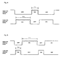
- the turn-ON time T2 of the lower side switching devices becomes long when the turn-ON time T1 of the upper side switching devices is short (i.e., when the ON duty ratio is small), as shown in FIG. 4 , and the turn-ON time T2 of the lower side switching devices becomes short when the turn-ON time T1 of the upper side switching devices is long (i.e., when the ON duty ratio is large), as shown in FIG. 5 .
- the turn-ON time T2 of the lower side switching devices is long and thus the phase current flowing through the current detection resistance through the switching device can be accurately detected; whereas in the case of FIG. 5 . the turn-ON time T2 of the lower side switching device is short, and thus the phase current flowing through the current detection resistance through the switching device becomes difficult to detect accurately. That is, as disclosed in Japanese Laid-Open Patent Publication No. 2003-164159 , when the duty ratio of the lower side switching devices becomes smaller than 30%, the switching devices may not be sufficiently turned ON due to obtuseness etc. of the waveform of the gate voltage to be applied to the device, and the phase current cannot be accurately detected.
- the turn-ON time of the switching device becomes shorter than a time constant of a charging circuit, sample hold is not accurately performed, and the error occurs in the detection of the phase current.
- the sum of the current values of the respective phases detected by the current detection resistances does not become zero, and determination is sometimes made that failure has occurred.
- the sum of the currents does not become zero because the phase currents cannot be accurately detected since the duty ratio of the lower side switching devices is small, and not because abnormality is found in the motor 4 and the drive circuit, and thus the determination is an erroneous determination.
- a multi-phase AC motor driving device that serves as a basis of the present invention includes an inverter circuit for driving a motor; a current detecting section for detecting a phase current of the motor; a control section for controlling a switching device of the inverter circuit; and a first determining section for determining occurrence of a failure.
- the inverter circuit includes pairs of upper and lower arms provided in association with respective phases of a motor, the inverter circuit being constituted such that the respective arm has a switching device for driving a multi-phase AC motor and a reflux diode connected in parallel to the device, and a voltage for driving the motor is extracted from a connection point of the upper and lower arms of the respective phases.
- the current detecting section arranged in the lower arm of the respective phase of the inverter circuit, detects a phase current of the motor.
- the control section controls ON/OFF operation of each switching device of the inverter circuit with a predetermined duty ratio.
- the first determining section determines occurrence of a failure based on a current value detected by the current detecting section.
- a second determining section for determining whether or not all ON-duty ratios of the switching devices of the upper arms of the inverter circuit are smaller than a predetermined value is arranged.
- the first determining section does not make a determination on the occurrence of the failure if the second determining section determines that the ON- duty ratios are not smaller than the predetermined value, and the first determining section makes a determination on the occurrence of the failure if the second determining section determines that the ON-duty ratios are smaller than the predetermined value.
- the ON-duty ratios of the upper side switching devices are large, that is, if the ON-duty ratios of the lower side switching devices are small, the failure diagnosis based on the detected current values is not performed even if the currents flowing during a short turn-ON period of the lower side switching devices are detected by the current detecting section, and thus erroneous determination that failure has occurred is not made, and the reliability of the device can be enhanced.
- the second determining section compares an absolute value of the current value of one phase and an absolute value of a sum of the current values of the other phases if only the ON-duty ratio of the switching device of the upper arm of one phase is greater than or equal to the predetermined value, and determines an error in a detection result of the current value of the one phase if the absolute value of the current value of the one phase is larger than the absolute value of the sum of the current values of the other phases or the second determining section compares an absolute value of a sum of the current values of a plurality of phases and an absolute value of the current value of the other one phase if the ON-duty ratios of the switching devices of the upper arms of the plurality of phases excluding one phase is greater than or equal to the predetermined value, and determines an error in a detection result of the current values of the plurality of phases if the absolute value of the sum of the current values of the plurality of phases is larger than the predetermined value
- the failure diagnosis is not performed when the ON-duty ratios of the lower side switching devices are small and the phase current cannot be accurately detected, and thus erroneous determination that failure has occurred is not made and the reliability of the device can be enhanced.
- FIG. 1 shows a view of an electrical structure of a multi-phase AC motor driving device according to the embodiment of the present invention.
- the electrical structure of a multi-phase AC motor driving device includes a control portion 1 constituted by a CPU, a memory and the like; a known PWM circuit 2 which outputs PWM signals having predetermined duty ratios based on command voltages Vu to Vw from the control portion 1; an inverter circuit 3 which outputs motor-driving three-phase voltages (U-phase voltage, V-phase voltage, W-phase voltage) based on the PWM signals from the PWM circuit 2; a three-phase AC motor 4 (hereinafter simply referred to as "motor”) driven by the three-phase voltage output from the inverter circuit 3; windings 4u, 4v, and 4w of the respective phases of the motor 4; sample-and-hold circuits 5u, 5v, and 5w which sample voltage for detecting the phase currents over a predetermined period and holds the sample; and DC amplification circuits 6u,
- a large current open/close switch may be used in place of the relay.
- the control portion 1, the PWM circuit 2, the inverter circuit 3, the sample-and-hold circuits 5u, 5v, and 5w, the DC amplification circuits 6u, 6v, and 6w, and the relays K1, K2, and K3 configure the motor driving device.
- the inverter circuit 3 is connected between a positive electrode and a negative electrode (ground) of the battery E and converts the DC voltage of the battery E into an AC voltage.
- This inverter circuit 3 is a known circuit, and includes pairs of upper and lower arms provided in association with the U-phase, the V-phase, and the W-phase, the respective arms including switching devices Q1 to Q6, and reflux diodes D1 to D6 connected in parallel to the respective switching devices.
- the switching devices Q1 to Q6 are constituted by MOS FETs (Field Effect Transistors), but instead thereof, IGBTs (Insulated Gate Bipolar Mode Transistor) or other devices can be employed.
- the respective gates of the switching device Q1 to Q6 are individually provided with six types of PWM signals (U-phase upper, U-phase lower, V-phase upper, V-phase lower, W-phase upper, W-phase lower) from the PWM circuit 2.
- PWM signals U-phase upper, U-phase lower, V-phase upper, V-phase lower, W-phase upper, W-phase lower
- the switching devices Q1 to Q6 are turned ON (conduction state)
- the switching devices Q1 to Q6 are turned OFF (cut-off state).
- the U-phase voltage, the V-phase voltage, and the W-phase voltage for driving the motor are extracted from the connection points a, c, and e between the upper and lower arms of the respective phases in the inverter circuit 3 and are supplied to the motor 4.
- the U-phase voltage is extracted from the connection point a between the switching devices Q1, Q2 and is supplied to the U-phase winding 4u of the motor 4 through the relay K1.
- the V-phase voltage is extracted from the connection point c between the switching devices Q3, Q4 and is supplied to the V-phase winding 4v of the motor 4 through the relay K2.
- the W-phase voltage is extracted from the connection point e between the switching devices Q5, Q6 and is supplied to the W-phase winding 4w of the motor 4 through the relay K3.
- the motor 4 is constituted by, for example, a three-phase brushless motor.
- the current detection resistance Ru is connected in series with the switching devices Q1, Q2, and the voltage generated across the opposite ends of the resistance Ru (electric potential at point b) is input to the sample-and-hold circuit 5u.
- the current detection resistance Rv is connected in series with the switching devices Q3, Q4, and the voltage generated across opposite ends of the resistance Rv (electric potential at point d) is input to the sample-and-hold circuit 5v.
- the current detection circuit Rw is connected in series with the switching devices Q5, Q6, and the voltage generated across opposite ends of the resistance Rw (electric potential at point f) is input to the sample-and-hold circuit 5w.
- the sample-and-hold circuits 5u, 5v, and 5w include switches Su, Sv, Sw; condensers Cu, Cv, Cw; and differential amplifiers Au, Av, Aw.
- switches Su, Sv, Sw When currents flow through the current detection resistances Ru, Rv, and Rw in the inverter circuit 3, and, thus, the voltages to be detected are generated between the opposite ends of the resistances, the switches Su, Sv, and Sw are set to ON through sampling signals SPu, SPv, SPw from the control portion 1, and the voltages to be detected are sampled in such a way that they charge the condensers Cu, Cv, Cw through the switches Su, Sv, and Sw being turned ON.
- phase currents lu, lv, lw indicate the values of actual currents flowing through the respective phases of the motor 4, and are supplied to the control portion 1 as phase current detection values.
- the control portion 1 calculates the currents to be flowed through the respective phases of the motor 4, that is, the target values of the motor currents for providing a required steering aiding force, based on a torque value detected by a torque sensor (not illustrated) and a vehicle speed value detected by a vehicle speed sensor (not illustrated), and makes comparison between the target values and the phase currents lu, lv, lw (detected values) to determine the deviations therebetween. Then, based on the resultant deviations, the control portion 1 calculates command voltages Vu, Vv, and Vw for the respective phases which are to be supplied to the PWM circuit 2.
- the command voltages are parameters for performing feedback control such that currents having the target values flow through the windings 4u, 4v, and 4w of the respective phases in the motor 4.
- the PWM circuit 2 creates six types of PWM signals having predetermined duty ratios as described above, based on the command voltage, such that a U-phase voltage, a V-phase voltage, and a W-phase voltage corresponding to the command voltages Vu, Vv, Vw are supplied to the motor 4, and then supplies them to the respective switching device Q1 to Q6 of the inverter circuit 3.
- the control portion 1 outputs a relay control signal for controlling ON/OFF of each relay K1, K2, and K3.
- the current detection resistances Ru, Rv, Rw configure one embodiment of the current detecting section in the present invention
- the control portion 1 configures one embodiment of a first determining section and a second determining section in the present invention
- the control portion 1 and the PWM circuit 2 configure one embodiment of a control section in the present invention.
- step S1 the U-phase current lu flowing through the current detection resistance Ru is detected by the sample-and-hold circuit 5u and the DC amplification circuit 6u based on the electric potential at point b.
- step S2 the V-phase current lv flowing through the current detection resistance Rv is detected by the sample-and-hold circuit 5v and the DC amplification circuit 6v based on the electric potential at point d.
- step S3 the W-phase current lw flowing through the current detection resistance Rw is detected by the sample-and-hold circuit 5w and the DC amplification circuit 6w based on the electric potential at point f.
- step S4 whether or not all the ON duty ratios of the switching devices Q1, Q3, and Q5 on the upper side in the inverter circuit 3 are smaller than 70% is determined.
- the ON duty ratios of the switching devices Q1, Q3, and Q5 can be judged by checking what command voltage is being supplied from the control portion 1 to the PWM circuit 2 by the control portion 1 itself. If the ON duty ratios of the upper side switching devices Q1, Q3, and Q5 are smaller than 70% as a result of the determination in step S4, in other words, if the ON duty ratios of the switching devices Q2, Q4 and Q6 on the lower side are greater than or equal to 30% (step S4: YES), the process proceeds to a failure diagnosis process of steps S5 to S7.
- step S6 the absolute value
- of I obtained in step S5 and a predetermined value ⁇ are compared. Since the sum of the currents of the respective phases of the motor is theoretically zero, the value of ⁇ is ideally ⁇ 0, but actually, it is a value containing slight error difference. If not
- step S6 determines whether the operation of the motor driving device is stopped. If
- step S4 If the ON duty ratios of the upper side switching devices Q1, Q3, and Q5 are not smaller than 70% as a result of the determination in step S4, in other words, if the ON duty ratios of the lower side switching devices Q2, Q4, and Q6 are smaller than 30% (step S4: NO), the process is terminated without executing the failure diagnosis process of steps S5 to S7.
- This aspect is the characteristic of the present embodiment, and erroneous determination on the occurrence of failure can be avoided.
- the period in which the current flows through the current detection resistances Ru, Rv, and Rw does not satisfy the charge time constant of the condensers Cu, Cv, Cw of the sample-and-hold circuits 5u, 5v, and 5w since the turn-ON time of the devices is short.
- the voltage generated in the current detection resistances Ru, Rv, and Rw is not accurately sampled and held in the condensers Cu, Cv, and Cw, and an error occurs in the values of the phase currents lu, lv, and lw output from the DC amplification circuits 6u, 6v, and 6w.
- the failure diagnosis process is performed in this case, the sum lu + lv + lw of the current values of the respective phases does not become zero, and erroneous determination that failure has occurred might be made.
- the failure diagnosis based on the current values is not performed if the failure diagnosis process is prohibited when the ON duty ratios of the lower side switching devices Q2, Q4, and Q6 are smaller than 30%, and thus erroneous determination that failure has occurred is not made, and the reliability of the device can be enhanced.
- FIG. 3 is a flowchart showing other procedures of the failure diagnosis.
- same reference numerals are denoted for steps performing the same process as in FIG. 2 .
- Steps S1 to S7 are exactly the same as FIG. 2 . That is, the U-phase current lu is detected in step S1, the V-phase current lv is detected in step S2, and the W-phase current lw is detected in step S3, and thereafter, whether or not all the ON duty ratios of the upper side switching devices Q1, Q3, and Q5 are smaller than 70% is determined, where if smaller than 70% (step S4: YES), the failure diagnosis process of steps S5 to S7 is executed.
- step S4 YES
- step S4: NO the process is terminated without performing the failure diagnosis if the ON duty ratios are not smaller than 70% (step S4: NO) in step S4, but in FIG. 3 , the processes of steps S8 to S13 are added if the ON duty ratios are not smaller than 70% (step S4: NO).
- step S8 whether or not the upper side switching devices which ON duty ratios are greater than or equal to 70% is only one is determined. If only one (step S8: YES), whether or not the relationship of iA > > iB + iC that is, the relationship of
- ⁇ is a threshold value set in advance.
- the process proceeds to step S10 if the relationship of equation (1) is met (step S9: YES), and the process is terminated without executing step S10 if the relationship is not met (step S9: NO).
- step S10 determination is made that there is an error in the current detection result of the A phase when the relationship of equation (1) is met.
- the reliability of the detected current value iA of the A phase is low since the ON duty ratio of the upper side switching device of the A phase is greater than or equal to 70% (ON duty ratio of the lower side switching device is smaller than 30%).
- the detected current values iB and iC of the B phase and the C phase are reliable values since the ON duty ratios of the upper side switching devices of the B phase and the C phase are smaller than 70% (ON duty ratio of the lower side switching devices are greater than or equal to 30%).
- the detected current value iA of the A phase is clearly abnormal if the absolute value of iA is extremely large compared to the absolute value of iB + iC as in equation (1) when iA and iB + iC are compared.
- the control portion 1 determines that the failure occurred in the circuit of A phase and that the detected current value iA of the A phase is an error, and performs processes such as failure signal output and the like. Error in the detection result of the current value can be judged on a specific phase which ON duty ratio of the upper side switching device is greater than or equal to 70% even if the failure determination of steps S5 to S7 is not performed.
- step S8 NO
- step S11 whether or not the upper side switching devices which ON duty ratios are greater than or equal to 70% are two is determined. If two (step S11: YES), whether or not the relationship iD + iE > > iF that is, the relationship of
- ⁇ is a threshold value set in advance.
- step S13 if the relationship of equation (2) is met (step S12: YES), and the process is terminated without executing step S13 if the relationship is not met (step S12: NO).
- step S13 determination is made that there is an error in the current detection result of the D phase or the E phase when the relationship of equation (2) is met.
- the reliability of the detected current values iD and iE of the D phase and the E phase is low since the ON duty ratios of the upper side switching devices of the D phase and the E phase are greater than or equal to 70% (ON duty ratios of the lower side switching device are smaller than 30%).
- the detected current value iF of the F phase is a reliable value since the ON duty ratio of the upper side switching devices of the F phase is smaller than 70% (ON duty ratio of the lower side switching devices are greater than or equal to 30%).
- the detected current values iD and iE of the D phase and the E phase are clearly abnormal if the absolute value of iD + iE is extremely large compared to the absolute value of iF as in equation (2) when iD + iE and iF are compared.
- the control portion 1 determines that the failure occurred in the circuit of D phase or E phase and that the detected current value iD, iE of the relevant phase is an error, and performs processes such as failure signal output and the like. Error in the detection result of the current value can be judged on a specific plurality of phases which ON duty ratios of the upper side switching devices are greater than or equal to 70% even if the failure determination of steps S5 to S7 is not performed.
- a brushless motor has been described for the motor 4 by way of example, but the present invention is applicable to motor driving devices in general for driving an AC motor with a plurality of phases such as an induction motor and a synchronous motor.
Landscapes
- Engineering & Computer Science (AREA)
- Chemical & Material Sciences (AREA)
- Combustion & Propulsion (AREA)
- Transportation (AREA)
- Mechanical Engineering (AREA)
- Control Of Ac Motors In General (AREA)
- Inverter Devices (AREA)
- Control Of Motors That Do Not Use Commutators (AREA)
- Control Of Multiple Motors (AREA)
Claims (1)
- Mehrphasige Wechsetstrom-Motorantriebsvorrichtung, umfassend:eine Inverterschaltung (3), welche Paare oberer und unterer Zweige aufweist, die in Verbindung mit jeweiligen Phasen eines Motors (4) vorgesehen sind, wobei die Inverterschaltung derart gebildet ist, dass der jeweilige Zweig eine Schalteinrichtung (Q1-Q6) zum Ansteuern eines mehrphasigen Wechselstrommotors und eine zu der Einrichtung parallel geschaltete Rücklaufdiode (D1-D6) aufweist, und eine Spannung zum Ansteuern des Motors von einer Verbindungsstelle der oberen und der unteren Zweige der jeweiligen Phasen entnommen wird;einen Stromermittlungsabschnitt (Ru, Rv, Rw), welcher in dem unteren Zweig der jeweiligen Phase der Inverterschaltung angeordnet ist, zur Ermittlung eines Phasenstroms des Motors;einen Steuerungsabschnitt (1, 2) zur Steuerung eines EIN/AUS-Betriebs jeder Schalteinrichtung der Inverterschaltung mit einer vorbestimmten relativen Einschaltdauer; undeinen ersten Bestimmungsabschnitt zur Bestimmung des Auftretens eines Fehlers basierend auf einem Stromwert, der von dem Stromermittlungsabschnitt ermittelt wird; wobei die mehrphasige Wechselstrom-Motorantriebsvorrichtung ferner umfasst:einen zweiten Bestimmungsabschnitt zur Bestimmung, ob alle EIN-Betriebsanteile der Schalteinrichtungen der oberen Zweige der Inverterschaltung kleiner als ein vorbestimmter Wert sind oder nicht; wobeider erste Bestimmungsabschnitt keine Bestimmung über das Auftreten des Fehlers durchführt, wenn der zweite Bestimmungsabschnitt bestimmt, dass die EIN-Betriebsanteile nicht geringer als der vorbestimmte Wert sind; undder erste Bestimmungsabschnitt eine Bestimmung über das Auftreten des Fehlers durchführt, wenn der zweite Bestimmungsabschnitt bestimmt, dass die EIN-Betriebsanteile geringer als der vorbestimmte Wert sind, wobeiim Falle, dass bestimmt wird, dass die EIN-Betriebsanteile nicht geringer als der vorbestimmte Wert sind, der zweite Bestimmungsabschnitteinen absoluten Wert des Stromwerts einer Phase und einen absoluten Wert (|I|) einer Summe der Stromwerte der anderen Phasen vergleicht, wenn nur der EIN-Betriebsanteil der Schalteinrichtung des oberen Zweigs einer Phase größer als oder gleich dem vorbestimmten Wert ist, und einen Fehler in einem Ermittlungsergebnis des Stromwerts der einen Phase bestimmt, wenn der absolute Wert des Stromwerts der einen Phase größer als der absolute Wert der Summe der Stromwerte der anderen Phasen ist, odereinen absoluten Wert einer Summe der Stromwerte einer Vielzahl von Phasen und einen absoluten Wert des Stromwerts der einen anderen Phase vergleicht, wenn die EIN-Betriebsanteile der Schalteinrichtungen der oberen Zweige der Vielzahl von Phasen ausschließlich einer Phase größer als oder gleich dem vorbestimmten Wert sind, und einen Fehler in einem Ermittlungsergebnis der Stromwerte der Vielzahl von Phasen bestimmt, wenn der absolute Wert der Summe der Stromwerte der Vielzahl von Phasen größer als der absolute Wert des Stromwerts der einen anderen Phase ist.
Applications Claiming Priority (2)
| Application Number | Priority Date | Filing Date | Title |
|---|---|---|---|
| JP2007236126A JP5014034B2 (ja) | 2007-09-12 | 2007-09-12 | 多相交流モータ駆動装置 |
| JP2007237426A JP5057908B2 (ja) | 2007-09-13 | 2007-09-13 | 多相交流モータ駆動装置 |
Publications (2)
| Publication Number | Publication Date |
|---|---|
| EP2037565A1 EP2037565A1 (de) | 2009-03-18 |
| EP2037565B1 true EP2037565B1 (de) | 2011-02-23 |
Family
ID=40229858
Family Applications (1)
| Application Number | Title | Priority Date | Filing Date |
|---|---|---|---|
| EP08159428A Not-in-force EP2037565B1 (de) | 2007-09-12 | 2008-07-01 | Mehrphasige Wechselstrom-Motorantriebsvorrichtung |
Country Status (3)
| Country | Link |
|---|---|
| EP (1) | EP2037565B1 (de) |
| AT (1) | ATE499740T1 (de) |
| DE (1) | DE602008005074D1 (de) |
Families Citing this family (2)
| Publication number | Priority date | Publication date | Assignee | Title |
|---|---|---|---|---|
| CN109768757B (zh) * | 2016-12-21 | 2022-09-06 | 上海理工大学 | 多相交流电机、逆变器、电驱动组件以及电动装置 |
| DE102019205471A1 (de) * | 2019-04-16 | 2020-10-22 | Robert Bosch Gmbh | Verfahren zum Überprüfen von Messwerten von Stromstärken von Strömen, die von einem sechsphasigen Stromrichter an wenigstens eine elektrische Maschine bereitgestellt werden |
Family Cites Families (11)
| Publication number | Priority date | Publication date | Assignee | Title |
|---|---|---|---|---|
| DE4009184A1 (de) * | 1990-03-22 | 1991-09-26 | Heidelberger Druckmasch Ag | Verfahren zur unterdrueckung von stromspitzen waehrend einer kommutierung eines buerstenlosen gleichstrommotors |
| JPH06253585A (ja) | 1993-02-25 | 1994-09-09 | Nippondenso Co Ltd | ブラシレスモータの異常検出装置 |
| JP2001314089A (ja) * | 2000-04-27 | 2001-11-09 | Matsushita Electric Ind Co Ltd | インバータ制御回路 |
| US7068191B2 (en) * | 2001-08-01 | 2006-06-27 | Ebm-Papst St.Georgen Gmbh & Co. Kg | Method for determining the numerical value for the duration of a periodically repeated pulse signal, and device for carrying out said method |
| CN1473391B (zh) * | 2001-09-29 | 2012-09-26 | 大金工业株式会社 | 相电流检测方法及相电流检测装置 |
| JP3674578B2 (ja) | 2001-11-29 | 2005-07-20 | 株式会社デンソー | 三相インバータの電流検出装置 |
| KR100459127B1 (ko) * | 2002-05-06 | 2004-12-03 | 엘지전자 주식회사 | 모터의 상 전류 검출 장치 및 그 방법 |
| JP2005059786A (ja) * | 2003-08-18 | 2005-03-10 | Koyo Seiko Co Ltd | 電動パワーステアリング装置 |
| JP4378151B2 (ja) | 2003-11-04 | 2009-12-02 | 株式会社デンソー | モータ駆動装置 |
| JP4422567B2 (ja) * | 2004-06-30 | 2010-02-24 | 株式会社日立製作所 | モータ駆動装置,電動アクチュエータおよび電動パワーステアリング装置 |
| JP5230068B2 (ja) | 2006-01-13 | 2013-07-10 | オムロンオートモーティブエレクトロニクス株式会社 | インバータ装置 |
-
2008
- 2008-07-01 DE DE602008005074T patent/DE602008005074D1/de active Active
- 2008-07-01 AT AT08159428T patent/ATE499740T1/de not_active IP Right Cessation
- 2008-07-01 EP EP08159428A patent/EP2037565B1/de not_active Not-in-force
Also Published As
| Publication number | Publication date |
|---|---|
| DE602008005074D1 (de) | 2011-04-07 |
| ATE499740T1 (de) | 2011-03-15 |
| EP2037565A1 (de) | 2009-03-18 |
Similar Documents
| Publication | Publication Date | Title |
|---|---|---|
| US7948205B2 (en) | Multi-phase AC motor driving device | |
| EP2037566B1 (de) | Mehrphasige Wechselstrom-Motorantriebsvorrichtung | |
| JP5142917B2 (ja) | 多相モータ駆動装置 | |
| EP1808955B1 (de) | Umrichtervorrichtung | |
| EP3193443A1 (de) | Wechselrichtervorrichtung zur ansteuerung eines mehrphasigen wechselstrommotors | |
| EP1832885A1 (de) | Vorrichtung zur Erdfehlerdetektion für eine Motorantriebsschaltung | |
| EP2299587A2 (de) | Motorantriebsvorrichtung geeignet, einen Fehlerzustand zu erkennen | |
| US10071762B2 (en) | Detection and mitigation of inverter errors in steering system motors | |
| US20150280609A1 (en) | Load driving device | |
| CN107112922B (zh) | 变流器和用于运行变流器的方法 | |
| KR20150122069A (ko) | 전동기 구동 장치 | |
| JP2006320176A (ja) | インバータの診断方法及び装置 | |
| EP3404827A1 (de) | Elektromotorsteuerungsvorrichtung | |
| EP2571158B1 (de) | Bürstenloser antrieb | |
| EP3367548A1 (de) | Wechselrichterschaltung, motorsteuergerät und servolenksystem | |
| US20110285334A1 (en) | Method for operating a brushless motor | |
| EP2037565B1 (de) | Mehrphasige Wechselstrom-Motorantriebsvorrichtung | |
| EP2073370B1 (de) | Motorsteuereinrichtung | |
| JP6131874B2 (ja) | インバータ回路の故障検出方法、駆動装置及びモータ駆動システム | |
| CN118044092A (zh) | 电力供给装置 | |
| JP2021191074A (ja) | インバータ制御装置 |
Legal Events
| Date | Code | Title | Description |
|---|---|---|---|
| PUAI | Public reference made under article 153(3) epc to a published international application that has entered the european phase |
Free format text: ORIGINAL CODE: 0009012 |
|
| AK | Designated contracting states |
Kind code of ref document: A1 Designated state(s): AT BE BG CH CY CZ DE DK EE ES FI FR GB GR HR HU IE IS IT LI LT LU LV MC MT NL NO PL PT RO SE SI SK TR |
|
| AX | Request for extension of the european patent |
Extension state: AL BA MK RS |
|
| RIN1 | Information on inventor provided before grant (corrected) |
Inventor name: GUNJI, KEITA, C/O OMRON CORPORATION |
|
| 17P | Request for examination filed |
Effective date: 20090915 |
|
| 17Q | First examination report despatched |
Effective date: 20091007 |
|
| AKX | Designation fees paid |
Designated state(s): AT BE BG CH CY CZ DE DK EE ES FI FR GB GR HR HU IE IS IT LI LT LU LV MC MT NL NO PL PT RO SE SI SK TR |
|
| GRAP | Despatch of communication of intention to grant a patent |
Free format text: ORIGINAL CODE: EPIDOSNIGR1 |
|
| RAP1 | Party data changed (applicant data changed or rights of an application transferred) |
Owner name: OMRON AUTOMOTIVE ELECTRONICS CO., LTD. |
|
| GRAS | Grant fee paid |
Free format text: ORIGINAL CODE: EPIDOSNIGR3 |
|
| GRAA | (expected) grant |
Free format text: ORIGINAL CODE: 0009210 |
|
| AK | Designated contracting states |
Kind code of ref document: B1 Designated state(s): AT BE BG CH CY CZ DE DK EE ES FI FR GB GR HR HU IE IS IT LI LT LU LV MC MT NL NO PL PT RO SE SI SK TR |
|
| REG | Reference to a national code |
Ref country code: GB Ref legal event code: FG4D |
|
| REG | Reference to a national code |
Ref country code: CH Ref legal event code: EP |
|
| REG | Reference to a national code |
Ref country code: IE Ref legal event code: FG4D |
|
| REF | Corresponds to: |
Ref document number: 602008005074 Country of ref document: DE Date of ref document: 20110407 Kind code of ref document: P |
|
| REG | Reference to a national code |
Ref country code: DE Ref legal event code: R096 Ref document number: 602008005074 Country of ref document: DE Effective date: 20110407 |
|
| REG | Reference to a national code |
Ref country code: NL Ref legal event code: VDEP Effective date: 20110223 |
|
| LTIE | Lt: invalidation of european patent or patent extension |
Effective date: 20110223 |
|
| PG25 | Lapsed in a contracting state [announced via postgrant information from national office to epo] |
Ref country code: PT Free format text: LAPSE BECAUSE OF FAILURE TO SUBMIT A TRANSLATION OF THE DESCRIPTION OR TO PAY THE FEE WITHIN THE PRESCRIBED TIME-LIMIT Effective date: 20110623 Ref country code: SE Free format text: LAPSE BECAUSE OF FAILURE TO SUBMIT A TRANSLATION OF THE DESCRIPTION OR TO PAY THE FEE WITHIN THE PRESCRIBED TIME-LIMIT Effective date: 20110223 Ref country code: LV Free format text: LAPSE BECAUSE OF FAILURE TO SUBMIT A TRANSLATION OF THE DESCRIPTION OR TO PAY THE FEE WITHIN THE PRESCRIBED TIME-LIMIT Effective date: 20110223 Ref country code: ES Free format text: LAPSE BECAUSE OF FAILURE TO SUBMIT A TRANSLATION OF THE DESCRIPTION OR TO PAY THE FEE WITHIN THE PRESCRIBED TIME-LIMIT Effective date: 20110603 Ref country code: LT Free format text: LAPSE BECAUSE OF FAILURE TO SUBMIT A TRANSLATION OF THE DESCRIPTION OR TO PAY THE FEE WITHIN THE PRESCRIBED TIME-LIMIT Effective date: 20110223 Ref country code: NO Free format text: LAPSE BECAUSE OF FAILURE TO SUBMIT A TRANSLATION OF THE DESCRIPTION OR TO PAY THE FEE WITHIN THE PRESCRIBED TIME-LIMIT Effective date: 20110523 Ref country code: GR Free format text: LAPSE BECAUSE OF FAILURE TO SUBMIT A TRANSLATION OF THE DESCRIPTION OR TO PAY THE FEE WITHIN THE PRESCRIBED TIME-LIMIT Effective date: 20110524 Ref country code: HR Free format text: LAPSE BECAUSE OF FAILURE TO SUBMIT A TRANSLATION OF THE DESCRIPTION OR TO PAY THE FEE WITHIN THE PRESCRIBED TIME-LIMIT Effective date: 20110223 |
|
| PG25 | Lapsed in a contracting state [announced via postgrant information from national office to epo] |
Ref country code: NL Free format text: LAPSE BECAUSE OF FAILURE TO SUBMIT A TRANSLATION OF THE DESCRIPTION OR TO PAY THE FEE WITHIN THE PRESCRIBED TIME-LIMIT Effective date: 20110223 Ref country code: CY Free format text: LAPSE BECAUSE OF FAILURE TO SUBMIT A TRANSLATION OF THE DESCRIPTION OR TO PAY THE FEE WITHIN THE PRESCRIBED TIME-LIMIT Effective date: 20110223 Ref country code: BG Free format text: LAPSE BECAUSE OF FAILURE TO SUBMIT A TRANSLATION OF THE DESCRIPTION OR TO PAY THE FEE WITHIN THE PRESCRIBED TIME-LIMIT Effective date: 20110523 Ref country code: SI Free format text: LAPSE BECAUSE OF FAILURE TO SUBMIT A TRANSLATION OF THE DESCRIPTION OR TO PAY THE FEE WITHIN THE PRESCRIBED TIME-LIMIT Effective date: 20110223 Ref country code: FI Free format text: LAPSE BECAUSE OF FAILURE TO SUBMIT A TRANSLATION OF THE DESCRIPTION OR TO PAY THE FEE WITHIN THE PRESCRIBED TIME-LIMIT Effective date: 20110223 Ref country code: BE Free format text: LAPSE BECAUSE OF FAILURE TO SUBMIT A TRANSLATION OF THE DESCRIPTION OR TO PAY THE FEE WITHIN THE PRESCRIBED TIME-LIMIT Effective date: 20110223 Ref country code: AT Free format text: LAPSE BECAUSE OF FAILURE TO SUBMIT A TRANSLATION OF THE DESCRIPTION OR TO PAY THE FEE WITHIN THE PRESCRIBED TIME-LIMIT Effective date: 20110223 |
|
| PG25 | Lapsed in a contracting state [announced via postgrant information from national office to epo] |
Ref country code: DK Free format text: LAPSE BECAUSE OF FAILURE TO SUBMIT A TRANSLATION OF THE DESCRIPTION OR TO PAY THE FEE WITHIN THE PRESCRIBED TIME-LIMIT Effective date: 20110223 Ref country code: EE Free format text: LAPSE BECAUSE OF FAILURE TO SUBMIT A TRANSLATION OF THE DESCRIPTION OR TO PAY THE FEE WITHIN THE PRESCRIBED TIME-LIMIT Effective date: 20110223 |
|
| PG25 | Lapsed in a contracting state [announced via postgrant information from national office to epo] |
Ref country code: SK Free format text: LAPSE BECAUSE OF FAILURE TO SUBMIT A TRANSLATION OF THE DESCRIPTION OR TO PAY THE FEE WITHIN THE PRESCRIBED TIME-LIMIT Effective date: 20110223 Ref country code: RO Free format text: LAPSE BECAUSE OF FAILURE TO SUBMIT A TRANSLATION OF THE DESCRIPTION OR TO PAY THE FEE WITHIN THE PRESCRIBED TIME-LIMIT Effective date: 20110223 Ref country code: CZ Free format text: LAPSE BECAUSE OF FAILURE TO SUBMIT A TRANSLATION OF THE DESCRIPTION OR TO PAY THE FEE WITHIN THE PRESCRIBED TIME-LIMIT Effective date: 20110223 |
|
| PG25 | Lapsed in a contracting state [announced via postgrant information from national office to epo] |
Ref country code: MT Free format text: LAPSE BECAUSE OF FAILURE TO SUBMIT A TRANSLATION OF THE DESCRIPTION OR TO PAY THE FEE WITHIN THE PRESCRIBED TIME-LIMIT Effective date: 20110223 |
|
| PLBE | No opposition filed within time limit |
Free format text: ORIGINAL CODE: 0009261 |
|
| STAA | Information on the status of an ep patent application or granted ep patent |
Free format text: STATUS: NO OPPOSITION FILED WITHIN TIME LIMIT |
|
| 26N | No opposition filed |
Effective date: 20111124 |
|
| PG25 | Lapsed in a contracting state [announced via postgrant information from national office to epo] |
Ref country code: MC Free format text: LAPSE BECAUSE OF NON-PAYMENT OF DUE FEES Effective date: 20110731 Ref country code: PL Free format text: LAPSE BECAUSE OF FAILURE TO SUBMIT A TRANSLATION OF THE DESCRIPTION OR TO PAY THE FEE WITHIN THE PRESCRIBED TIME-LIMIT Effective date: 20110223 |
|
| REG | Reference to a national code |
Ref country code: DE Ref legal event code: R097 Ref document number: 602008005074 Country of ref document: DE Effective date: 20111124 |
|
| REG | Reference to a national code |
Ref country code: IE Ref legal event code: MM4A |
|
| PG25 | Lapsed in a contracting state [announced via postgrant information from national office to epo] |
Ref country code: IT Free format text: LAPSE BECAUSE OF FAILURE TO SUBMIT A TRANSLATION OF THE DESCRIPTION OR TO PAY THE FEE WITHIN THE PRESCRIBED TIME-LIMIT Effective date: 20110223 |
|
| PG25 | Lapsed in a contracting state [announced via postgrant information from national office to epo] |
Ref country code: IE Free format text: LAPSE BECAUSE OF NON-PAYMENT OF DUE FEES Effective date: 20110701 |
|
| PGFP | Annual fee paid to national office [announced via postgrant information from national office to epo] |
Ref country code: GB Payment date: 20120627 Year of fee payment: 5 |
|
| REG | Reference to a national code |
Ref country code: DE Ref legal event code: R082 Ref document number: 602008005074 Country of ref document: DE Representative=s name: KILIAN KILIAN & PARTNER MBB PATENTANWAELTE, DE Ref country code: DE Ref legal event code: R082 Ref document number: 602008005074 Country of ref document: DE Representative=s name: KILIAN KILIAN & PARTNER, DE |
|
| REG | Reference to a national code |
Ref country code: CH Ref legal event code: PL |
|
| PG25 | Lapsed in a contracting state [announced via postgrant information from national office to epo] |
Ref country code: CH Free format text: LAPSE BECAUSE OF NON-PAYMENT OF DUE FEES Effective date: 20120731 Ref country code: LI Free format text: LAPSE BECAUSE OF NON-PAYMENT OF DUE FEES Effective date: 20120731 |
|
| PG25 | Lapsed in a contracting state [announced via postgrant information from national office to epo] |
Ref country code: LU Free format text: LAPSE BECAUSE OF NON-PAYMENT OF DUE FEES Effective date: 20110701 |
|
| PG25 | Lapsed in a contracting state [announced via postgrant information from national office to epo] |
Ref country code: IS Free format text: LAPSE BECAUSE OF FAILURE TO SUBMIT A TRANSLATION OF THE DESCRIPTION OR TO PAY THE FEE WITHIN THE PRESCRIBED TIME-LIMIT Effective date: 20110223 |
|
| PG25 | Lapsed in a contracting state [announced via postgrant information from national office to epo] |
Ref country code: TR Free format text: LAPSE BECAUSE OF FAILURE TO SUBMIT A TRANSLATION OF THE DESCRIPTION OR TO PAY THE FEE WITHIN THE PRESCRIBED TIME-LIMIT Effective date: 20110223 |
|
| PG25 | Lapsed in a contracting state [announced via postgrant information from national office to epo] |
Ref country code: HU Free format text: LAPSE BECAUSE OF FAILURE TO SUBMIT A TRANSLATION OF THE DESCRIPTION OR TO PAY THE FEE WITHIN THE PRESCRIBED TIME-LIMIT Effective date: 20110223 |
|
| GBPC | Gb: european patent ceased through non-payment of renewal fee |
Effective date: 20130701 |
|
| PG25 | Lapsed in a contracting state [announced via postgrant information from national office to epo] |
Ref country code: GB Free format text: LAPSE BECAUSE OF NON-PAYMENT OF DUE FEES Effective date: 20130701 |
|
| REG | Reference to a national code |
Ref country code: DE Ref legal event code: R084 Ref document number: 602008005074 Country of ref document: DE |
|
| REG | Reference to a national code |
Ref country code: DE Ref legal event code: R084 Ref document number: 602008005074 Country of ref document: DE Effective date: 20140717 |
|
| REG | Reference to a national code |
Ref country code: FR Ref legal event code: PLFP Year of fee payment: 9 |
|
| PGFP | Annual fee paid to national office [announced via postgrant information from national office to epo] |
Ref country code: FR Payment date: 20160613 Year of fee payment: 9 |
|
| REG | Reference to a national code |
Ref country code: FR Ref legal event code: ST Effective date: 20180330 |
|
| PG25 | Lapsed in a contracting state [announced via postgrant information from national office to epo] |
Ref country code: FR Free format text: LAPSE BECAUSE OF NON-PAYMENT OF DUE FEES Effective date: 20170731 |
|
| PGFP | Annual fee paid to national office [announced via postgrant information from national office to epo] |
Ref country code: DE Payment date: 20220531 Year of fee payment: 15 |
|
| REG | Reference to a national code |
Ref country code: DE Ref legal event code: R119 Ref document number: 602008005074 Country of ref document: DE |
|
| PG25 | Lapsed in a contracting state [announced via postgrant information from national office to epo] |
Ref country code: DE Free format text: LAPSE BECAUSE OF NON-PAYMENT OF DUE FEES Effective date: 20240201 |