EP2033147B1 - Verfahren zur integration einer identifikationsschaltung in ein datenmedium - Google Patents
Verfahren zur integration einer identifikationsschaltung in ein datenmedium Download PDFInfo
- Publication number
- EP2033147B1 EP2033147B1 EP07788997.0A EP07788997A EP2033147B1 EP 2033147 B1 EP2033147 B1 EP 2033147B1 EP 07788997 A EP07788997 A EP 07788997A EP 2033147 B1 EP2033147 B1 EP 2033147B1
- Authority
- EP
- European Patent Office
- Prior art keywords
- slot
- data
- circuit
- conductive layer
- resonating
- Prior art date
- Legal status (The legal status is an assumption and is not a legal conclusion. Google has not performed a legal analysis and makes no representation as to the accuracy of the status listed.)
- Ceased
Links
Images
Classifications
-
- G—PHYSICS
- G06—COMPUTING OR CALCULATING; COUNTING
- G06K—GRAPHICAL DATA READING; PRESENTATION OF DATA; RECORD CARRIERS; HANDLING RECORD CARRIERS
- G06K19/00—Record carriers for use with machines and with at least a part designed to carry digital markings
- G06K19/06—Record carriers for use with machines and with at least a part designed to carry digital markings characterised by the kind of the digital marking, e.g. shape, nature, code
- G06K19/067—Record carriers with conductive marks, printed circuits or semiconductor circuit elements, e.g. credit or identity cards also with resonating or responding marks without active components
- G06K19/07—Record carriers with conductive marks, printed circuits or semiconductor circuit elements, e.g. credit or identity cards also with resonating or responding marks without active components with integrated circuit chips
- G06K19/077—Constructional details, e.g. mounting of circuits in the carrier
- G06K19/07749—Constructional details, e.g. mounting of circuits in the carrier the record carrier being capable of non-contact communication, e.g. constructional details of the antenna of a non-contact smart card
-
- G—PHYSICS
- G06—COMPUTING OR CALCULATING; COUNTING
- G06K—GRAPHICAL DATA READING; PRESENTATION OF DATA; RECORD CARRIERS; HANDLING RECORD CARRIERS
- G06K19/00—Record carriers for use with machines and with at least a part designed to carry digital markings
- G06K19/04—Record carriers for use with machines and with at least a part designed to carry digital markings characterised by the shape
- G06K19/041—Constructional details
- G06K19/042—Constructional details the record carrier having a form factor of a credit card and including a small sized disc, e.g. a CD or DVD
- G06K19/045—Constructional details the record carrier having a form factor of a credit card and including a small sized disc, e.g. a CD or DVD the record carrier being of the non-contact type, e.g. RFID, and being specially adapted for attachment to a disc, e.g. a CD or DVD
-
- G—PHYSICS
- G11—INFORMATION STORAGE
- G11B—INFORMATION STORAGE BASED ON RELATIVE MOVEMENT BETWEEN RECORD CARRIER AND TRANSDUCER
- G11B23/00—Record carriers not specific to the method of recording or reproducing; Accessories, e.g. containers, specially adapted for co-operation with the recording or reproducing apparatus ; Intermediate mediums; Apparatus or processes specially adapted for their manufacture
- G11B23/0014—Record carriers not specific to the method of recording or reproducing; Accessories, e.g. containers, specially adapted for co-operation with the recording or reproducing apparatus ; Intermediate mediums; Apparatus or processes specially adapted for their manufacture record carriers not specifically of filamentary or web form
- G11B23/0021—Record carriers not specific to the method of recording or reproducing; Accessories, e.g. containers, specially adapted for co-operation with the recording or reproducing apparatus ; Intermediate mediums; Apparatus or processes specially adapted for their manufacture record carriers not specifically of filamentary or web form discs
- G11B23/0028—Details
- G11B23/0035—Details means incorporated in the disc, e.g. hub, to enable its guiding, loading or driving
- G11B23/0042—Details means incorporated in the disc, e.g. hub, to enable its guiding, loading or driving with provision for auxiliary features
-
- H—ELECTRICITY
- H01—ELECTRIC ELEMENTS
- H01Q—ANTENNAS, i.e. RADIO AERIALS
- H01Q1/00—Details of, or arrangements associated with, antennas
- H01Q1/12—Supports; Mounting means
- H01Q1/22—Supports; Mounting means by structural association with other equipment or articles
- H01Q1/2208—Supports; Mounting means by structural association with other equipment or articles associated with components used in interrogation type services, i.e. in systems for information exchange between an interrogator/reader and a tag/transponder, e.g. in Radio Frequency Identification [RFID] systems
-
- H—ELECTRICITY
- H01—ELECTRIC ELEMENTS
- H01Q—ANTENNAS, i.e. RADIO AERIALS
- H01Q13/00—Waveguide horns or mouths; Slot antennas; Leaky-waveguide antennas; Equivalent structures causing radiation along the transmission path of a guided wave
- H01Q13/10—Resonant slot antennas
Definitions
- the present invention relates to an improvement to data carriers, such as optical media. It relates more particularly to a method of manufacturing an optical data carrier for the integration of an electronic chip or "tag", more particularly a tag operating at RF frequency, inside the support.
- RFID technique The technique of identification at a distance or using radio frequencies known in Europe under the term “RFID technique” or in the United States under the term “RF technique” allows identification and, more general, the remote reading of information included in an integrated circuit or chip through an interrogation system using radio frequency waves called RFID reader ("RFID reader" in English).
- RFID reader radio frequency waves
- the integrated circuit is in the form of a chip connected to a transmitting / receiving antenna generally known by the term "RFID tag” and attached to an object.
- the RFID tag is activated when it enters the field generated by the "RFID reader" with which it is associated and returns to it the requested information and stored in the chip.
- RFID tags can be passive or active. Active tags are powered by a clean energy source such as a battery while passive tags receive energy from the radio frequency signal received by the tag.
- RFID can be used in a wide range of applications from labeling to product authentication to advanced logistics.
- optical discs such as compact discs (CDs) or digital versatile discs (DVDs)
- the use of an RFID tag may be useful for combating illegal copying and theft in stores.
- the tag is integrated into the structure of the optical disk and not simply attached, for example on the cover containing said disk.
- Reference 3 represents the dipole type antenna obtained by printing on the edge of the optical disk a line made using a conductive ink.
- Reference 4 represents the power supply of the antenna connected to an RFID chip.
- Reference 5 represents the central opening of the disc allowing it to be driven inside a reader.
- the antenna is constituted by one or more conducting rings made by the conductive layer of the structure of the optical disk which may be a CD or a DVD, these rings being coupled to the chip.
- the conductive layer is demetallized in places.
- This solution uses as antenna the conductive layer, especially the aluminum layer which is part of the structure of a CD or DVD.
- the present invention therefore proposes a novel solution for integrating a radio frequency chip or tag into the structure of an optical disk or the like, making it possible to overcome the drawbacks of the solutions of the prior art.
- the present invention more particularly relates to a method of producing the antenna structure in the data carrier and its coupling to the integrated circuit or chip.
- ⁇ g being a function of the effective permittivity of the slot, this value depending on the permittivity of the material, its thickness and also the width of the slot, it is therefore possible to modify the resonance frequency by adjusting the length and the width of the slot. slot.
- At least two concentric resonant slots electromagnetically coupled to one another are etched in the non-data portion of the conductive layer.
- At least two partially overlapping resonant slots are etched in the non-data portion of the conductive layer.
- the integrated circuit is electromagnetically coupled to the resonant slot.
- the integrated circuit can be coupled by direct connection to the slot.
- the integrated circuit is positioned on the resonant slot at a length L 'with respect to one of the ends of the resonant slot, so as to optimize the impedance of the resonant slot.
- the data carrier is an optical disc such as a compact disc (CD), a digital versatile disc (DVD), a mini-disc or the like.
- the integrated circuit or chip is an RFID circuit or an RF circuit.
- a data carrier consisting of an optical data carrier such as a compact disc (CD).
- CD compact disc
- DVDs versatile digital discs
- the structure of a compact disc or CD is well known to those skilled in the art and will not be described in great detail. It consists of a stack of at least one dielectric layer, more particularly a polycarbonate layer, in which are engraved "pits" representing the data. This layer is covered with a reflective layer, more particularly an aluminum layer, the latter being covered with a dielectric material, most often an UV lacquer acrylic creating a protective film for the data.
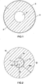
- a compact disc has the shape of an aluminum ring 10 which, in the context of the present invention, comprises a first ring 10a receiving the data and a second ring 10b which is a part without data.
- the portion without data is at the inner ring.
- the disk has a central hole 11 for mounting it on the axis of rotation of a reader.
- the central hole 11 has a radius r i .
- This radius r i determines the inner perimeter of the ring without data which extends to a circle of radius r im such that the ring of the part without data extends over a width equal to r im - i .
- a slot 12 having a length L less than the perimeter determined by the radius r im has been etched a slot 12 having a length L less than the perimeter determined by the radius r im .
- the length 13 in the area without data extending the slot 12 is a metallized area.
- a radiating antenna has been provided in a non-data portion of the optical disk, preferably a portion located near the center of rotation of the disk. The dimensions of this part without data can be limited by the outer perimeter of the radiating antenna.
- the slot 12 is supplied at a point 14.
- the supply of the slot is made by electromagnetic coupling by placing the chip or RFID tag 14 in parallel on the slot.
- the RFID tag instead of being connected by an electromagnetic coupling to the resonant slot 12, can be connected directly to the slot.
- the connection point is chosen to correspond to the impedance point of the slot which ensures the best energy transmission from the antenna to the chip and vice versa.
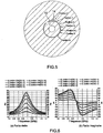
- a CD disk with a resonant slot antenna as shown in the figures 2 and 3 was simulated using commercial electromagnetic software (IE3D from Zeland). The following parameters were used for the simulation.
- the optical disk consists of a polycarbonate substrate having a thickness of 0.6 mm, a permittivity ( ⁇ r) of 2.8 and a tan ⁇ 1e -4.
- the polycarbonate substrate is covered with an aluminum layer having a conductivity of 38000000 Siemens / m and a thickness of 50 nm.
- the inner radius r i of the metal disk is 7.5 mm while the outer radius R of the disk is 60 mm.
- a resonant slot 12 has been etched in the aluminum layer. This slot 12 has a length L equal to 115 mm to obtain a resonance around 950 MHz. This slot is written here in the circle of radius r im less than or equal to 20mm.
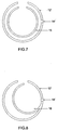
- the disk With the disk as described above, it was first simulated frequency responses impedance (real and imaginary part) of the slot for several slot widths ranging between 0.5 mm and 3.5 mm. The results of the simulation are given at figure 4 . Indeed, the adjustment of the width of the slot makes it possible to adjust the impedance of the antenna. However, since a modification of the width of the slot causes a change in the resonant frequency, as follows from the applications given above, it is therefore possible to modify the resonance frequency by adjusting the length of the slot. load presented by the RFID tag and using the figure 4 It is then possible to choose the slot width to present the conjugated impedance of the RFID tag, to better adapt the antenna to the RFID circuit.
- the width of the slot is one of the means for controlling the impedance of the antenna to be presented to the RFID tag, and this for a position of the excitation of the given slot.
- the RFID tag is coupled in parallel to the resonant slot 12. To obtain the best coupling possible, it must take place at a length L 'of one end of the slot which is chosen so as to optimize this coupling. To determine this optimal position, different positions were simulated using the software mentioned above, this simulation being necessary to determine the optimal position because the slot is not rectilinear.
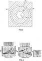
- a first resonant slot 12 'producing an antenna in accordance with the present invention is shown very schematically.
- this slot 12 ' has been mounted in parallel a tag or RFID chip 14', this tag being electromagnetically coupled to the resonant slot 12 '.
- a second slot 15 is made between the central hole and the slot 12 '.
- This slot 15 is a resonant slot that can be electromagnetically coupled to the slot 12 '.
- the second slot 15 is sized to resonate on another frequency, which makes it possible to obtain operation over several frequencies.
- a second slot 16 partially covers the first slot 12 'and develops inside the resonant slot 12'.
- This slot 16 provides flexibility at the level of adaptation of the tag or RFID chip 14 ', on several frequency bands.
- annular slots that can be added by proximity coupling to the main slot directly connected to the tag or RFID chip is not limited.
- the present invention has been described with reference to an optical disk such as a compact disc. However, it is obvious to one skilled in the art that it can be applied to other types of data carriers made of materials other than polycarbonate and aluminum provided that the substrate is a dielectric covered with metallization.
Landscapes
- Engineering & Computer Science (AREA)
- Physics & Mathematics (AREA)
- General Physics & Mathematics (AREA)
- Theoretical Computer Science (AREA)
- Computer Hardware Design (AREA)
- Microelectronics & Electronic Packaging (AREA)
- Optical Record Carriers And Manufacture Thereof (AREA)
- Waveguide Aerials (AREA)
- Details Of Aerials (AREA)
Claims (9)
- Verfahren zur Integration einer Identifikationsschaltung in ein Datenmedium, gebildet aus mindestens einem dielektrischen Substrat, das mit einer leitenden Schicht überzogen ist, wobei die leitende Schicht (10) einen Abschnitt umfasst, der Daten empfängt (10A) und einen Abschnitt ohne Daten (10B), dadurch gekennzeichnet, dass es umfasst:- Ätzen in dem Abschnitt ohne Daten (10B) der leitenden Schicht mindestens eines abstrahlenden Schlitzes, der eine Antenne bildet, durch Ätzen des Schlitzes auf einer Länge L, die derart ist, dass L=λg/2 oder Ag gleich der Wellenlänge in dem Schlitz mit der Resonanzfrequenz ist, und einer Breite, die derart ist, dass die Resonanzfrequenz mit der Arbeitsfrequenz der Identifikationsschaltung übereinstimmt, und- Koppeln einer integrierten Schaltung an den Schlitz.
- Verfahren nach Anspruch 1, dadurch gekennzeichnet, dass mindestens 2 konzentrische Resonanzschlitze (12', 15), die elektromagnetisch miteinander gekoppelt sind, in dem Abschnitt ohne Daten der leitenden Schicht geätzt werden.
- Verfahren nach Anspruch 1, dadurch gekennzeichnet, dass mindestens 2 Resonanzschlitze (12', 16), die sich teilweise überlappen, in dem Abschnitt ohne Daten der leitenden Schicht geätzt werden.
- Verfahren nach einem der Ansprüche 1 bis 3, dadurch gekennzeichnet, dass die integrierte Schaltung (14, 14') elektromagnetisch an den Resonanzschlitz gekoppelt ist.
- Verfahren nach einem der Ansprüche 1 bis 3, dadurch gekennzeichnet, dass die integrierte Schaltung direkt an den Resonanzschlitz angeschlossen ist.
- Verfahren nach einem der Ansprüche 1 bis 3, dadurch gekennzeichnet, dass die integrierte Schaltung auf dem Resonanzschlitz mit einer Länge L' in Bezug auf ein Ende des Resonanzschlitzes positioniert ist, den Scheinwiderstand des Resonanzschlitzes optimierend.
- Verfahren nach einem der Ansprüche 1 bis 6, dadurch gekennzeichnet, dass das Datenmedium eine Disc von der Art einer Compact Disc (CD), einer Digital Versatile Disc (DVD), einer Minidisc ist.
- Verfahren nach einem der Ansprüche 1 bis 7, dadurch gekennzeichnet, dass die integrierte Schaltung eine Schaltung von der Art einer RFID-Schaltung, einer RF-Schaltung ist.
- Datenmedium, dadurch gekennzeichnet, dass es entsprechend dem Verfahren der Ansprüche 1 bis 8 ausgeführt wird.
Applications Claiming Priority (2)
| Application Number | Priority Date | Filing Date | Title |
|---|---|---|---|
| FR0605830A FR2903216A1 (fr) | 2006-06-28 | 2006-06-28 | Perfectionnement aux supports de donnees tels que les supports optiques |
| PCT/FR2007/051431 WO2008000991A1 (fr) | 2006-06-28 | 2007-06-13 | Procede d'integration d'un circuit d'identification dans un support de donnees |
Publications (3)
| Publication Number | Publication Date |
|---|---|
| EP2033147A1 EP2033147A1 (de) | 2009-03-11 |
| EP2033147B1 true EP2033147B1 (de) | 2018-09-26 |
| EP2033147B8 EP2033147B8 (de) | 2018-10-31 |
Family
ID=37684893
Family Applications (1)
| Application Number | Title | Priority Date | Filing Date |
|---|---|---|---|
| EP07788997.0A Ceased EP2033147B8 (de) | 2006-06-28 | 2007-06-13 | Verfahren zur integration einer identifikationsschaltung in ein datenmedium |
Country Status (5)
| Country | Link |
|---|---|
| US (1) | US8502677B2 (de) |
| EP (1) | EP2033147B8 (de) |
| FR (1) | FR2903216A1 (de) |
| TW (1) | TWI402830B (de) |
| WO (1) | WO2008000991A1 (de) |
Families Citing this family (6)
| Publication number | Priority date | Publication date | Assignee | Title |
|---|---|---|---|---|
| WO2008005028A1 (en) | 2006-06-30 | 2008-01-10 | Thomson Licensing | Radio frequency transponder for use with a medium |
| US8963688B2 (en) * | 2012-08-20 | 2015-02-24 | The Goodyear Tire & Rubber Company | Stacked tire RFID reader system and method |
| US9043875B2 (en) * | 2013-03-01 | 2015-05-26 | Microsoft Technology Licensing, Llc | Contactless authentication of optical disk drives |
| US10181065B2 (en) * | 2016-10-28 | 2019-01-15 | University Of Florida Research Foundation, Incorporated | Unclonable environmentally-sensitive chipless RFID tag with a plurality of slot resonators |
| US10929741B2 (en) | 2018-06-18 | 2021-02-23 | University Of Florida Research Foundation, Incorporated | Cross-registration for unclonable chipless RFID tags |
| JP7470526B2 (ja) * | 2020-02-19 | 2024-04-18 | 大王製紙株式会社 | Rfidタグ、及びアンテナ |
Family Cites Families (13)
| Publication number | Priority date | Publication date | Assignee | Title |
|---|---|---|---|---|
| JP3373753B2 (ja) * | 1997-03-28 | 2003-02-04 | 株式会社東芝 | 超高周波帯無線通信装置 |
| US6081239A (en) * | 1998-10-23 | 2000-06-27 | Gradient Technologies, Llc | Planar antenna including a superstrate lens having an effective dielectric constant |
| US6329950B1 (en) * | 1999-12-06 | 2001-12-11 | Integral Technologies, Inc. | Planar antenna comprising two joined conducting regions with coax |
| MXPA02012930A (es) * | 2000-07-13 | 2003-10-14 | Thomson Licensing Sa | Antena plana de bandas multiples. |
| US6806842B2 (en) * | 2000-07-18 | 2004-10-19 | Marconi Intellectual Property (Us) Inc. | Wireless communication device and method for discs |
| FR2825206A1 (fr) * | 2001-05-23 | 2002-11-29 | Thomson Licensing Sa | Dispositif pour la reception et/ou l'emission d'ondes electromagnetiques a rayonnement omnidirectionnel |
| DE60323221D1 (de) * | 2002-04-24 | 2008-10-09 | Mineral Lassen Llc | Energiequellenkommunikation mit einer schlitzantenne |
| US20040052203A1 (en) * | 2002-09-13 | 2004-03-18 | Brollier Brian W. | Light enabled RFID in information disks |
| US7443299B2 (en) * | 2003-04-25 | 2008-10-28 | Avery Dennison Corporation | Extended range RFID system |
| DE602004017840D1 (de) * | 2004-05-17 | 2009-01-02 | Sony Dadc Austria Ag | Optischer Datenträger, Verfahren und Vorrichtung zur Herstellung eines optischen Datenträgers |
| JP4375147B2 (ja) * | 2004-07-16 | 2009-12-02 | ソニー株式会社 | 光ディスク記録再生装置およびコンテンツ管理方法 |
| JP4092510B2 (ja) * | 2004-10-28 | 2008-05-28 | ティアック株式会社 | 光ディスク検査装置、光ディスク検査方法、光ディスク検査用コンピュータプログラム |
| US7501947B2 (en) * | 2005-05-04 | 2009-03-10 | Tc License, Ltd. | RFID tag with small aperture antenna |
-
2006
- 2006-06-28 FR FR0605830A patent/FR2903216A1/fr not_active Withdrawn
-
2007
- 2007-06-08 TW TW096120621A patent/TWI402830B/zh not_active IP Right Cessation
- 2007-06-13 EP EP07788997.0A patent/EP2033147B8/de not_active Ceased
- 2007-06-13 US US12/308,724 patent/US8502677B2/en not_active Expired - Fee Related
- 2007-06-13 WO PCT/FR2007/051431 patent/WO2008000991A1/fr not_active Ceased
Non-Patent Citations (1)
| Title |
|---|
| None * |
Also Published As
| Publication number | Publication date |
|---|---|
| TWI402830B (zh) | 2013-07-21 |
| EP2033147A1 (de) | 2009-03-11 |
| TW200809842A (en) | 2008-02-16 |
| US20100045438A1 (en) | 2010-02-25 |
| WO2008000991A1 (fr) | 2008-01-03 |
| FR2903216A1 (fr) | 2008-01-04 |
| EP2033147B8 (de) | 2018-10-31 |
| US8502677B2 (en) | 2013-08-06 |
Similar Documents
| Publication | Publication Date | Title |
|---|---|---|
| EP1617506B1 (de) | Antennenstruktur für Funketikett für optisches Aufzeichnungsmedium | |
| EP2019998B1 (de) | Label mit einer hf-antidiebstahlantenne und uhf-rfid-transponder | |
| US8098133B2 (en) | Radio frequency identification tag | |
| WO2008000991A1 (fr) | Procede d'integration d'un circuit d'identification dans un support de donnees | |
| EP1407512B1 (de) | Antenne | |
| EP2622685B1 (de) | Breitbandantennereflektor für eine zirkular polarisierte flachdrahtantenne und verfahren zur herstellung dieses antennenreflektors | |
| EP2410470B1 (de) | Vorrichtung mit Mikroschaltkreis, die Verstärkungsmittel zur Verstärkung einer Antenne umfasst | |
| EP1275082B1 (de) | Elektronisches etikett | |
| WO2010066955A1 (fr) | Circuit d'antenne rfid | |
| EP2067115B1 (de) | Verfahren und system zum optimierten lesen eines hochfrequenzkommunikationstransponders mit hilfe eines passiven resonanzschaltkreises | |
| CN1781115A (zh) | 范围扩展的rfid系统 | |
| FR2963696A1 (fr) | Dispositif a microcircuit comprenant un circuit d'antenne de communication en champ proche | |
| EP2710522A1 (de) | Drahtkondensator, insbesondere für eine radiofrequenzschaltung, und vorrichtung mit diesem drahtkondensator | |
| FR2887712A1 (fr) | Procede et systeme de lecture optimisee de transpondeur de communication radio frequence a l'aide d'un circuit resonant passif | |
| EP1837811B1 (de) | Verfahren zur Herstellung eines elektronischen RFID-Etiketts | |
| EP1201007B1 (de) | Antenne für kontaktlose chipkarte, hybridkarten und elektronische etiketten | |
| JP4644742B2 (ja) | 光記録媒体用の無線タグアンテナ構造 | |
| EP2471030B1 (de) | Vorrichtung mit einer relais-antenne, zugehörige radiofrequenzvorrichtung und zugehöriges verfahren | |
| WO2022258909A1 (fr) | Dispositif répéteur de champ magnétique de communication en champ proche | |
| FR2950744A1 (fr) | Dispositif electronique sans contact a antenne de communication en champ proche | |
| WO2002037606A1 (fr) | Antenne multibande | |
| EP2525305A1 (de) | Fadenkondensator, insbesondere für Funkschaltkreis, und diesen umfassende Vorrichtung | |
| EP2624670A1 (de) | Fadenkondensator, insbesondere für Funkschaltkreis, und diesen umfassende Vorrichtung |
Legal Events
| Date | Code | Title | Description |
|---|---|---|---|
| PUAI | Public reference made under article 153(3) epc to a published international application that has entered the european phase |
Free format text: ORIGINAL CODE: 0009012 |
|
| 17P | Request for examination filed |
Effective date: 20081126 |
|
| AK | Designated contracting states |
Kind code of ref document: A1 Designated state(s): AT BE BG CH CY CZ DE DK EE ES FI FR GB GR HU IE IS IT LI LT LU LV MC MT NL PL PT RO SE SI SK TR |
|
| AX | Request for extension of the european patent |
Extension state: AL BA HR MK RS |
|
| 17Q | First examination report despatched |
Effective date: 20090420 |
|
| DAX | Request for extension of the european patent (deleted) | ||
| RBV | Designated contracting states (corrected) |
Designated state(s): DE FR GB |
|
| RAP1 | Party data changed (applicant data changed or rights of an application transferred) |
Owner name: THOMSON LICENSING |
|
| RAP1 | Party data changed (applicant data changed or rights of an application transferred) |
Owner name: THOMSON LICENSING DTV |
|
| GRAP | Despatch of communication of intention to grant a patent |
Free format text: ORIGINAL CODE: EPIDOSNIGR1 |
|
| STAA | Information on the status of an ep patent application or granted ep patent |
Free format text: STATUS: GRANT OF PATENT IS INTENDED |
|
| INTG | Intention to grant announced |
Effective date: 20180219 |
|
| GRAJ | Information related to disapproval of communication of intention to grant by the applicant or resumption of examination proceedings by the epo deleted |
Free format text: ORIGINAL CODE: EPIDOSDIGR1 |
|
| STAA | Information on the status of an ep patent application or granted ep patent |
Free format text: STATUS: EXAMINATION IS IN PROGRESS |
|
| INTC | Intention to grant announced (deleted) | ||
| GRAR | Information related to intention to grant a patent recorded |
Free format text: ORIGINAL CODE: EPIDOSNIGR71 |
|
| GRAS | Grant fee paid |
Free format text: ORIGINAL CODE: EPIDOSNIGR3 |
|
| STAA | Information on the status of an ep patent application or granted ep patent |
Free format text: STATUS: GRANT OF PATENT IS INTENDED |
|
| GRAA | (expected) grant |
Free format text: ORIGINAL CODE: 0009210 |
|
| STAA | Information on the status of an ep patent application or granted ep patent |
Free format text: STATUS: THE PATENT HAS BEEN GRANTED |
|
| INTG | Intention to grant announced |
Effective date: 20180815 |
|
| AK | Designated contracting states |
Kind code of ref document: B1 Designated state(s): DE FR GB |
|
| REG | Reference to a national code |
Ref country code: GB Ref legal event code: FG4D Free format text: NOT ENGLISH |
|
| RAP2 | Party data changed (patent owner data changed or rights of a patent transferred) |
Owner name: INTERDIGITAL MADISON PATENT HOLDINGS |
|
| REG | Reference to a national code |
Ref country code: DE Ref legal event code: R096 Ref document number: 602007056285 Country of ref document: DE |
|
| REG | Reference to a national code |
Ref country code: DE Ref legal event code: R097 Ref document number: 602007056285 Country of ref document: DE |
|
| PGFP | Annual fee paid to national office [announced via postgrant information from national office to epo] |
Ref country code: DE Payment date: 20190521 Year of fee payment: 13 |
|
| PLBE | No opposition filed within time limit |
Free format text: ORIGINAL CODE: 0009261 |
|
| STAA | Information on the status of an ep patent application or granted ep patent |
Free format text: STATUS: NO OPPOSITION FILED WITHIN TIME LIMIT |
|
| PGFP | Annual fee paid to national office [announced via postgrant information from national office to epo] |
Ref country code: FR Payment date: 20190522 Year of fee payment: 13 |
|
| 26N | No opposition filed |
Effective date: 20190627 |
|
| GBPC | Gb: european patent ceased through non-payment of renewal fee |
Effective date: 20190613 |
|
| PG25 | Lapsed in a contracting state [announced via postgrant information from national office to epo] |
Ref country code: GB Free format text: LAPSE BECAUSE OF NON-PAYMENT OF DUE FEES Effective date: 20190613 |
|
| REG | Reference to a national code |
Ref country code: DE Ref legal event code: R119 Ref document number: 602007056285 Country of ref document: DE |
|
| PG25 | Lapsed in a contracting state [announced via postgrant information from national office to epo] |
Ref country code: FR Free format text: LAPSE BECAUSE OF NON-PAYMENT OF DUE FEES Effective date: 20200630 |
|
| PG25 | Lapsed in a contracting state [announced via postgrant information from national office to epo] |
Ref country code: DE Free format text: LAPSE BECAUSE OF NON-PAYMENT OF DUE FEES Effective date: 20210101 |