EP2410470B1 - Vorrichtung mit Mikroschaltkreis, die Verstärkungsmittel zur Verstärkung einer Antenne umfasst - Google Patents
Vorrichtung mit Mikroschaltkreis, die Verstärkungsmittel zur Verstärkung einer Antenne umfasst Download PDFInfo
- Publication number
- EP2410470B1 EP2410470B1 EP11173386.1A EP11173386A EP2410470B1 EP 2410470 B1 EP2410470 B1 EP 2410470B1 EP 11173386 A EP11173386 A EP 11173386A EP 2410470 B1 EP2410470 B1 EP 2410470B1
- Authority
- EP
- European Patent Office
- Prior art keywords
- antenna
- foregoing
- module
- electrically conductive
- microcircuit
- Prior art date
- Legal status (The legal status is an assumption and is not a legal conclusion. Google has not performed a legal analysis and makes no representation as to the accuracy of the status listed.)
- Active
Links
- 238000004891 communication Methods 0.000 claims description 18
- 230000002093 peripheral effect Effects 0.000 claims description 18
- 238000004519 manufacturing process Methods 0.000 claims description 10
- 239000007769 metal material Substances 0.000 claims description 6
- 238000000034 method Methods 0.000 claims description 6
- 238000004804 winding Methods 0.000 claims description 6
- 230000009977 dual effect Effects 0.000 claims description 4
- 230000035699 permeability Effects 0.000 claims description 3
- 238000002955 isolation Methods 0.000 claims description 2
- 239000000758 substrate Substances 0.000 claims 4
- 238000012216 screening Methods 0.000 claims 1
- 238000007639 printing Methods 0.000 description 7
- 208000031968 Cadaver Diseases 0.000 description 6
- 238000007650 screen-printing Methods 0.000 description 6
- 239000000463 material Substances 0.000 description 5
- 210000000056 organ Anatomy 0.000 description 5
- 239000004033 plastic Substances 0.000 description 5
- 238000007493 shaping process Methods 0.000 description 5
- 230000008901 benefit Effects 0.000 description 4
- 238000005530 etching Methods 0.000 description 3
- 238000003475 lamination Methods 0.000 description 3
- 239000002184 metal Substances 0.000 description 3
- 229910052751 metal Inorganic materials 0.000 description 3
- RYGMFSIKBFXOCR-UHFFFAOYSA-N Copper Chemical compound [Cu] RYGMFSIKBFXOCR-UHFFFAOYSA-N 0.000 description 2
- 239000004593 Epoxy Substances 0.000 description 2
- BQCADISMDOOEFD-UHFFFAOYSA-N Silver Chemical compound [Ag] BQCADISMDOOEFD-UHFFFAOYSA-N 0.000 description 2
- 230000005465 channeling Effects 0.000 description 2
- 229910052802 copper Inorganic materials 0.000 description 2
- 239000010949 copper Substances 0.000 description 2
- 238000000151 deposition Methods 0.000 description 2
- 238000010292 electrical insulation Methods 0.000 description 2
- 230000004907 flux Effects 0.000 description 2
- 238000000465 moulding Methods 0.000 description 2
- 229910052709 silver Inorganic materials 0.000 description 2
- 239000004332 silver Substances 0.000 description 2
- 239000007787 solid Substances 0.000 description 2
- 239000004642 Polyimide Substances 0.000 description 1
- 239000000853 adhesive Substances 0.000 description 1
- 230000003321 amplification Effects 0.000 description 1
- 238000005452 bending Methods 0.000 description 1
- 239000011230 binding agent Substances 0.000 description 1
- 239000003795 chemical substances by application Substances 0.000 description 1
- 239000002131 composite material Substances 0.000 description 1
- 239000012141 concentrate Substances 0.000 description 1
- 229920001940 conductive polymer Polymers 0.000 description 1
- 230000008878 coupling Effects 0.000 description 1
- 238000010168 coupling process Methods 0.000 description 1
- 238000005859 coupling reaction Methods 0.000 description 1
- 230000008021 deposition Effects 0.000 description 1
- 230000005672 electromagnetic field Effects 0.000 description 1
- 238000004049 embossing Methods 0.000 description 1
- 238000005516 engineering process Methods 0.000 description 1
- 239000011152 fibreglass Substances 0.000 description 1
- PCHJSUWPFVWCPO-UHFFFAOYSA-N gold Chemical compound [Au] PCHJSUWPFVWCPO-UHFFFAOYSA-N 0.000 description 1
- 239000010931 gold Substances 0.000 description 1
- 229910052737 gold Inorganic materials 0.000 description 1
- 238000010348 incorporation Methods 0.000 description 1
- 238000003754 machining Methods 0.000 description 1
- 238000003801 milling Methods 0.000 description 1
- 230000004048 modification Effects 0.000 description 1
- 238000012986 modification Methods 0.000 description 1
- 238000003199 nucleic acid amplification method Methods 0.000 description 1
- 239000002245 particle Substances 0.000 description 1
- 239000000049 pigment Substances 0.000 description 1
- 229920000515 polycarbonate Polymers 0.000 description 1
- 239000004417 polycarbonate Substances 0.000 description 1
- 229920000728 polyester Polymers 0.000 description 1
- 229920001721 polyimide Polymers 0.000 description 1
- 229920000642 polymer Polymers 0.000 description 1
- 230000008569 process Effects 0.000 description 1
- 230000009467 reduction Effects 0.000 description 1
- 238000012360 testing method Methods 0.000 description 1
- 239000012815 thermoplastic material Substances 0.000 description 1
Images


Classifications
-
- G—PHYSICS
- G06—COMPUTING; CALCULATING OR COUNTING
- G06K—GRAPHICAL DATA READING; PRESENTATION OF DATA; RECORD CARRIERS; HANDLING RECORD CARRIERS
- G06K19/00—Record carriers for use with machines and with at least a part designed to carry digital markings
- G06K19/06—Record carriers for use with machines and with at least a part designed to carry digital markings characterised by the kind of the digital marking, e.g. shape, nature, code
- G06K19/067—Record carriers with conductive marks, printed circuits or semiconductor circuit elements, e.g. credit or identity cards also with resonating or responding marks without active components
- G06K19/07—Record carriers with conductive marks, printed circuits or semiconductor circuit elements, e.g. credit or identity cards also with resonating or responding marks without active components with integrated circuit chips
- G06K19/077—Constructional details, e.g. mounting of circuits in the carrier
- G06K19/07749—Constructional details, e.g. mounting of circuits in the carrier the record carrier being capable of non-contact communication, e.g. constructional details of the antenna of a non-contact smart card
- G06K19/0775—Constructional details, e.g. mounting of circuits in the carrier the record carrier being capable of non-contact communication, e.g. constructional details of the antenna of a non-contact smart card arrangements for connecting the integrated circuit to the antenna
- G06K19/07756—Constructional details, e.g. mounting of circuits in the carrier the record carrier being capable of non-contact communication, e.g. constructional details of the antenna of a non-contact smart card arrangements for connecting the integrated circuit to the antenna the connection being non-galvanic, e.g. capacitive
-
- G—PHYSICS
- G06—COMPUTING; CALCULATING OR COUNTING
- G06K—GRAPHICAL DATA READING; PRESENTATION OF DATA; RECORD CARRIERS; HANDLING RECORD CARRIERS
- G06K19/00—Record carriers for use with machines and with at least a part designed to carry digital markings
- G06K19/06—Record carriers for use with machines and with at least a part designed to carry digital markings characterised by the kind of the digital marking, e.g. shape, nature, code
- G06K19/067—Record carriers with conductive marks, printed circuits or semiconductor circuit elements, e.g. credit or identity cards also with resonating or responding marks without active components
- G06K19/07—Record carriers with conductive marks, printed circuits or semiconductor circuit elements, e.g. credit or identity cards also with resonating or responding marks without active components with integrated circuit chips
- G06K19/077—Constructional details, e.g. mounting of circuits in the carrier
- G06K19/07749—Constructional details, e.g. mounting of circuits in the carrier the record carrier being capable of non-contact communication, e.g. constructional details of the antenna of a non-contact smart card
- G06K19/07773—Antenna details
- G06K19/07775—Antenna details the antenna being on-chip
-
- G—PHYSICS
- G06—COMPUTING; CALCULATING OR COUNTING
- G06K—GRAPHICAL DATA READING; PRESENTATION OF DATA; RECORD CARRIERS; HANDLING RECORD CARRIERS
- G06K19/00—Record carriers for use with machines and with at least a part designed to carry digital markings
- G06K19/06—Record carriers for use with machines and with at least a part designed to carry digital markings characterised by the kind of the digital marking, e.g. shape, nature, code
- G06K19/067—Record carriers with conductive marks, printed circuits or semiconductor circuit elements, e.g. credit or identity cards also with resonating or responding marks without active components
- G06K19/07—Record carriers with conductive marks, printed circuits or semiconductor circuit elements, e.g. credit or identity cards also with resonating or responding marks without active components with integrated circuit chips
- G06K19/077—Constructional details, e.g. mounting of circuits in the carrier
- G06K19/07749—Constructional details, e.g. mounting of circuits in the carrier the record carrier being capable of non-contact communication, e.g. constructional details of the antenna of a non-contact smart card
- G06K19/07773—Antenna details
- G06K19/07777—Antenna details the antenna being of the inductive type
- G06K19/07779—Antenna details the antenna being of the inductive type the inductive antenna being a coil
- G06K19/07783—Antenna details the antenna being of the inductive type the inductive antenna being a coil the coil being planar
-
- Y—GENERAL TAGGING OF NEW TECHNOLOGICAL DEVELOPMENTS; GENERAL TAGGING OF CROSS-SECTIONAL TECHNOLOGIES SPANNING OVER SEVERAL SECTIONS OF THE IPC; TECHNICAL SUBJECTS COVERED BY FORMER USPC CROSS-REFERENCE ART COLLECTIONS [XRACs] AND DIGESTS
- Y10—TECHNICAL SUBJECTS COVERED BY FORMER USPC
- Y10T—TECHNICAL SUBJECTS COVERED BY FORMER US CLASSIFICATION
- Y10T29/00—Metal working
- Y10T29/49—Method of mechanical manufacture
- Y10T29/49002—Electrical device making
- Y10T29/49016—Antenna or wave energy "plumbing" making
Definitions
- the present invention relates to the technical field of portable electronic non-contact type devices comprising a near-field communication antenna connected to a microcircuit, enabling the establishment of a contactless communication with an external device.
- the invention applies more particularly, but not exclusively, to microcircuit cards provided with an antenna, such as so-called non-contact cards making it possible to establish contactless communication at a predefined operating frequency, for example 13.56 MHz defined. by the ISO 14 443 standard, or the so-called hybrid or dual cards, allowing to establish both a contactless communication and a contact communication via an interface of external contacts able to come into contact with a adapted reader.
- a predefined operating frequency for example 13.56 MHz defined. by the ISO 14 443 standard, or the so-called hybrid or dual cards, allowing to establish both a contactless communication and a contact communication via an interface of external contacts able to come into contact with a adapted reader.
- the invention also applies to any type of portable or pocket electronic devices incorporating such an antenna, such as a USB key, an RFID (Radio Frequency IDentity) tag, a passport, etc.
- an antenna such as a USB key, an RFID (Radio Frequency IDentity) tag, a passport, etc.
- the near field communication antenna is generally formed by an electrically conductive wire wound into a plurality of electrically conductive turns, incorporated at the periphery of the body of the card to optimize the dimensions of the antenna and thus the range of the electronic device .
- an electronic device such as a dual-type microcircuit card comprising an antenna connected to a microcircuit.
- the card comprises a body provided with a receiving cavity of a module carrying the microcircuit.
- the body also incorporates the antenna which is connected to the microcircuit via two metal pads carried by the support.
- the junction obtained is more or less reliable, in particular because it can be weakened during bending or twisting of the card body that can lead to false contacts and short circuits between the circuits. internal microcircuit and the antenna.
- EP1031939 discloses a composite microcircuit module in which a coupler serves to power a second coupler for contactless communication.
- US2004 / 046663 discloses an RFID tag communicating with a passive loop by coupling.
- the invention particularly aims to provide a contactless card comprising a near field communication antenna for a reliable connection of the antenna and the microcircuit while being simple to achieve.
- the subject of the invention is an electronic device comprising a microcircuit module, a near-field communication antenna electrically connected to the microcircuit of the module, delimiting an antenna surface, and a body incorporating the module, the antenna. being arranged on a support of the module, the body incorporating antenna gain amplifying means comprising an electrically conductive member electrically isolated from the microcircuit and the antenna, of generally annular shape arranged around a region of the antenna. body forming a volume generated by the projection of the antenna surface along a direction substantially orthogonal to the surface, said member being formed by an electrically conductive layer traversed by a receiving cavity of the module formed in the body.
- the arrangement of the antenna in the module facilitates the realization of the junction between the microcircuit and the antenna.
- Such an arrangement of the antenna also makes it possible to overcome the conventional drawbacks related to a positioning of this antenna in the body of the device. Thanks to the invention, various printing operations, embossing, making a magnetic strip are independent of the position of the antenna in the device, which has many advantages, especially in the case of particular applications , such as in the field of smart cards.
- the invention proposes to add a device for amplifying the gain of the antenna in the body.
- the addition of such an electrically conductive member significantly increases the performance of the antenna by channeling the lines of the magnetic field emitted by an external terminal inside the antenna surface.
- the member forms an amplifier gain of the antenna improving the level of current induced in the latter and the retro-modulation level of the antenna when the device is placed in the electromagnetic field of the external terminal.
- the positioning in the body of this body does not have the aforementioned drawbacks in relation to the arrangement of the antenna in the body.
- the member extends around the antenna outside a region defined by the projection of the antenna along a direction substantially orthogonal to the antenna surface.
- the antenna and the ring must not extend vis-à-vis each other not to mask the magnetic field flux through the antenna surface.
- the member extends outside the outer contour of the antenna in a plane parallel to that containing the antenna or part of the antenna or possibly in the same plane.
- a minimum space is provided between the member and the antenna to provide electrical insulation.
- the member defines a peripheral inner edge surrounding the region with a minimized distance, for example less than or equal to five millimeters. It has thus been found that the smaller the distance separating the organ and the antenna, the better the performances. Thus, the distance can be substantially zero in the case where the antenna and the organ are in separate planes.
- the distance is minimized within the limit of a positioning tolerance of the antenna in the module.
- the antenna being formed by a winding of electrically conductive turns
- the positioning tolerance of the antenna in the module substantially corresponds to an interspire.
- the space between two turns is limited by the accuracy of realization of the antenna, for example an etching precision for electrical insulation of the two turns together.
- the module comprising a support carrying the microcircuit and the antenna
- the positioning tolerance of the antenna in the module substantially corresponds to the positioning tolerance of the antenna on the support.
- the subject of the invention is also a method of manufacturing a device according to the invention, comprising a step of shaping the support of the device and a step of forming the cavity in the body, characterized in that, when the step of forming the body, an electrically conductive layer is arranged in the body so that, during the cavity forming step, the cavity passes through the electrically conductive layer to form the body.
- FIG. 1 a microcircuit device according to the invention. This device is designated by the general reference 10.
- the microcircuit device 10 is a microcircuit card.
- the device 10 may be a page of a passport such as the cover of the passport or a self-adhesive label such as a "sticker".
- the device 10 comprises a body 12 in the general shape of a card delimiting first 12A and second 12B opposite faces.
- the body 12 delimits the external dimensions of the card 10.
- the dimensions of the card 10 are defined by the ID-1 format of the ISO 7816 standard, which is the conventionally used format. for bank cards of dimensions 86 mm by 54 mm and with a thickness substantially equal to eight hundred micrometers. Of course, other card formats may also be used.
- the card body 12 is shaped by lamination, that is to say by forming, for example by means of a press and in a hot lamination operation, a stack of layers or sheets. laminated for example made of thermoplastic material.
- the body 12 comprises a stack of at least three layers: a central layer 14 forming a data printing layer interposed between two transparent outer layers 16A, 16B.
- the central data printing layer 14 is itself formed of three sub-layers, a central sub-layer 14C forming "inlay" interposed between two other data printing sub-layers 14A, 14B.
- the two outer layers 16A, 16B are said to be "overlay" and serve, for example, to protect the data printed on the central layer 14C.
- the body has a thickness of eight hundred microns and the outer layers 16A, 16B have a thickness substantially between forty and eighty microns.
- the sub-layers 14A, 14B, 14C have thicknesses between 200 and 350 micrometers.
- the body 12 may comprise a central layer 14 comprising two sub-layers 14A and 14B, the set of two layers being interposed between two transparent layers 16A, 16B. More generally, the central layer 14 may comprise an underlayer or more than two sublayers.
- the layers 14, 16 are made of a material essentially comprising a plastic material such as polycarbonate, PVC, etc.
- the body 12 may be shaped by molding, for example plastic.
- the device 10 comprises a microcircuit 18 able to exchange with an external terminal, to process and / or store data.
- the body 12 incorporates a microcircuit module 20 comprising the microcircuit 18.
- the module 20 comprises a support 22 carrying the chip 18.
- the support 22 delimits first 22A and second 22B opposite faces, respectively said outer face and inner face, the outer face 22A being turned towards the outside of the card 10.
- the support 22 is, for example, made of fiberglass epoxy type, polyester or paper and has a thickness for example between fifty and two hundred micrometers.
- the support 22 is made of a plastic material essentially based on polyimide with a thickness of about seventy micrometers.
- the body 12 comprises a cavity 24 for housing the module 20.
- This cavity 24 is preferably formed in the body 12 and opens on one of the faces 12A, 12B of the body 12, for example the first face 12A.
- the module 20 may be incorporated in the body 12 for example to form a non-contact type device.
- the module 20 can be made invisible from the outside by opacification, for example with an opaque ink, layers surrounding it.
- the cavity 24 comprises for example a deep central zone 26 provided with a bottom 28 for housing the microcircuit 18 and a raised peripheral zone 30 with respect to the central zone 26 delimiting a step 29 with the bottom 28.
- This peripheral zone 30 comprises a raised bearing surface with respect to the bottom of the cavity 24 on which the edges of the support 22 of the module 20 ( figure 2 ).
- the card 10 comprises for example an external interface 32 of contact pads 34 electrically connected to the microcircuit 18.
- This interface 32 allows the establishment of a communication with contact of the card 10 with another terminal external, for example when the card 10 is inserted in a suitable card reader.
- the interface 32 comprises a series of metal contact pads 34, conforming to a predefined microcircuit card standard.
- the contact pads are in accordance with ISO 7816.
- the contacts 34 of the interface 32 correspond to the contacts C1, C2, C3, C5, C6, C7 of the ISO 7816 standard.
- the interface 32 of the card 10 is preferably made of a layer of metallic material such as copper but may also be made, alternatively, by screen printing of conductive ink such as epoxy ink loaded with silver particles or or by screen printing an electrically conductive polymer.
- the ranges are electrically connected to the microcircuit 18 by electrically conductive wires, such as, for example, gold wires passing through via made in the module support, themselves connected to electrically conductive tracks of connections extending on the inside of the support.
- the card 10 is of dual type, that is to say it comprises both a contactless interface capable of establishing a near-field communication with an external terminal and a suitable contact interface. to establish a communication with another external terminal by contact.
- the card can only be of contactless type.
- the card 10 is preferably devoid of the interface 32 of external contacts 34.
- the device 10 also comprises a connected near-field communication antenna 36. Electrically to the microcircuit 18.
- the antenna 36 comprises an outer contour delimiting an antenna surface S.
- the antenna 36 is arranged on the module 20.
- the antenna 36 is formed by a winding of electrically conductive turns.
- the antenna 36 is formed by a copper track.
- the antenna 36 preferably comprises a plurality of turns each having a width of the order of fifty to three hundred microns and the spacing between two contiguous turns is of the order of fifty to two hundred micrometers. Note by interspire the minimum spacing between two turns of the antenna 36.
- the antenna 36 extends on the support 22 and is formed by a winding of electrically conductive turns extending at the periphery of one of the faces of the support 22, for example the internal face 22B.
- the antenna 36 is for example made by depositing a metal, according to an etching or screen printing technology.
- the antenna 36 may also be formed by an electrically conductive wire in an insulating sheath.
- the antenna 36 extends in two parts 36A, 36B and at the periphery of the two opposite faces 22A, 22B of the module support 20, the two parts 36A, 36B being electrically connected to one another via at least one via V1, V2 passing through the support 22 of the module 20.
- the antenna portion 36A extends on the opposite face 22A to the face 22B carrying the microcircuit 18 and surrounds the interface 34.
- the support 22 of the module 20 has for example a generally rectangular shape and the antenna 36 along the periphery of the support 22.
- the support 22 may have any oblong shape.
- the support 22 has dimensions compatible with the known manufacturing processes and used to manufacture microcircuit cards, whether in length, width or thickness.
- the antenna 36 is in this embodiment formed by a winding of electrically conductive turns extending at the periphery of one of the faces 22A, 22B of the module support 20.
- the distance separating the antenna 36 from an outer contour of the face 22A, 22B of the support 22 is less than or equal to one interspire, that is to say the minimum spacing distance between two turns of the antenna 36.
- the body 12 also incorporates means 40 for amplifying the gain of the antenna 36 comprising an electrically conductive member 42 and electrically isolated from the microcircuit 18 and the antenna 36.
- means 40 for amplifying the gain of the antenna 36 comprising an electrically conductive member 42 and electrically isolated from the microcircuit 18 and the antenna 36.
- this member 42 is to concentrate or direct the field lines coming from the reader towards the antenna 36.
- This member 42 has, in accordance with the invention, and as illustrated on the Figures 1 and 2 , a generally annular shape and is arranged to surround a region R of the body 12 forming a volume generated by the projection of the antenna surface along a direction substantially orthogonal to the antenna surface S.
- the volume is also limited by the contour of the body 12.
- the surface S extends parallel to the two opposite faces 22A, 22B of the support 22 and the orthogonal direction Z substantially corresponds to the vertical direction of the support 22 and therefore the body 12 of the card 10.
- the member 42 forms a closed ring.
- the ring thus forms means for channeling the magnetic flux generated by the external terminal inside the antenna 36 in order to increase the gain of the antenna.
- the member 42 may form a ring interrupted at least once. It has been discovered that the production of an open ring further improves the performance of the antenna 36.
- the ring is shaped so that the device 10 operates at a communication frequency with an external terminal by example of 13.56 MHz.
- the presence of the ring is taken into account for adjusting the resonant frequency of the device.
- the antenna surface S substantially corresponds to the surface of the support 22 and the region R consequently has a transverse section substantially corresponding to the surface of the support 22.
- Ring 42 preferably has a general shape surrounding the substantially rectangular support.
- the member 42 is preferably made of a metallic material of relative magnetic permeability less than or equal to one.
- the member 42 is made of a material such as an electrically conductive ink.
- the ink comprises a binder agent based essentially on polymer and metallic pigments (for example silver). This ink is intended to be applied preferably in screen printing to form a film of thickness substantially between ten and twenty microns.
- the member 42 preferably extends as close as possible to the antenna 36 in a direction substantially transverse to the body 12 which corresponds to a horizontal direction of the body 12. performance as a function of the transverse distance between the antenna 36 and the member 42 is highlighted by the curve C1 of the graph of the figure 9 .
- the member 42 defines an inner peripheral edge 48 surrounding the region R with a minimized distance, for example less than or equal to five millimeters. For example, this distance is minimized within the limit of a positioning accuracy of the antenna 36 in the module 20.
- the positioning tolerance of the antenna 36 in the module 20 corresponds to the positioning tolerance of the antenna 36 on the support 22.
- the antenna 36 being formed by a winding of electrically conductive turns and the member 42 extending in the same plane as that containing the antenna 36 or at least a portion 36A, 36B of the antenna 36, the minimized distance is chosen to ensure electrical isolation of the antenna 36 and the member 42.
- the minimized distance is greater than or equal to an interspire.
- the member 42 defines an inner peripheral edge 48 surrounding the module 20, the inner edge 48 is at least partially at the surface of a peripheral wall of the cavity 24.
- the ring 42 surrounds the region R with a distance corresponding to the distance between the edge of the support 22 and the outer contour of the antenna 36.
- the member 42 extends, in this example, substantially in a plane of the device comprising the antenna 36 or a plane comprising at least one of the parts 36A, 36B of the antenna 36 when the latter is in two parts.
- the member 42 may extend in a plane substantially parallel to that or those containing the antenna 36, for example to meet specific spatial constraints of the device 10.
- the member 42 possibly being in a position visible from the outside of the device, for example by being printed on a visible face, through the outer layer. 16A or 16B, of a data printing layer 14.
- the thickness of the layers for example sub-layers of the central layer 14.
- the member 42 surrounds the lateral zone 30 of the cavity 24 in which the support 22 extends.
- the increase in the width L of the annular member 42 also improves the performance of the antenna 36 and in particular the range P (see figure 10 ).
- the figure 10 represents a graph comprising a curve C2 of evolution of the range P expressed in millimeters as a function of the width L of the member 42.
- the member 42 is solid pattern.
- the member 42 may be non-full pattern.
- the ring 42 forms a grid or a series of concentric rings with increasing circumferences, etc.
- This variant has the advantage of reducing the amount of conductive ink while maintaining RF performance equivalent to that of a solid pattern member.
- This variant also has the advantage of improving the bond between the layers, a grid pattern for increasing the plastic surface vis-à-vis.
- the organ 42 is designed to be used in a passport. It has a dimension substantially equivalent to that of a passport and a rectangular main opening of 27.2mm x 17.8mm dimension compatible with the size of a passport module.
- the position of the opening on the figure 12 achieves optimal contactless RF performance.
- the position of this opening on the figure 13 by bringing the antenna closer to the seam of the passport reduces the mechanical stresses supported by the antenna, during certification tests and when using the passport.
- the member 42 is designed to be used in an ID1 format card. It has a dimension substantially equivalent to that of a card in ID1 format and a rectangular main opening of 27.2mm x 17.8mm or 27.2mmx13.1mm size compatible with the module size of a card in ID1 format. Those skilled in the art will understand that the larger dimension improves non-contact RF performance.
- the method comprises, for example, a step of shaping the support 22 of the device 10.
- This shaping step can constitute either a lamination step of a plurality of layers between them, or a molding operation of the body in a plastic material.
- an electrically conductive layer is arranged in the body 12. This arrangement is provided so that, during the step of forming the cavity 24, the cavity 24 passes through the electrically conductive layer for forming the ring 42.
- the body 12 is formed by a multilayer structure, and the electrically conductive layer is interposed between two layers of the body 12.
- the electrically conductive layer is printed on one of the layers of the body 12 with an electrically conductive ink, for example by screen printing or by etching.
- the electrically conductive layer is printed on a data printing layer 14.
- This data printing layer 14 is delimited by a face visible from the outside of the device bearing data such as the name of a bank or an identification number of a card or any personal or informative data carried by the card and an opposite face hidden in the body 12, and the electrically conductive layer is carried by this hidden face, for example for aesthetic reasons.
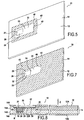
- the layer extends across the entire surface of the body as shown in the figure 7 .
- This embodiment makes it possible to obtain a member 42 with a maximum width L and thus to further improve performance.
- the member 42 obtained extends closer to the peripheral wall of the cavity 24 and therefore of the antenna 36 in a transverse direction of the body 12. It is then possible to obtain a precise adjustment of the position of the ring 42 with respect to the antenna 36. Indeed, the antenna 36 extends at the periphery of the support 22 of the module 20, for example with a tolerance of positioning less than or equal to an interspire.
- the member 42 extends around the cavity 24 at a substantially zero distance since the ring 42 is flush with the wall of the cavity 24.
- the distance in a transverse direction of the body 12 between the member 42 and the antenna 36 may be less than or equal to the positioning tolerance of the antenna 36 on the support 42, and therefore less than or equal to an interspire.
- the device obtained is more resistant in particular to folding because of the grouping of sensitive components such as the antenna and the microcircuit in the module.
- the invention has been described more particularly for a card in the forma ID-1. It can be applied to any hand-held electronic device, portable or otherwise, using a near-field communication antenna whose gain is sought to be increased.
- the device forms an inlay having a thickness of, for example, between 300 and 400 micrometers.
Claims (21)
- Elektronische Vorrichtung (10), umfassend ein Modul (20) mit Mikroschaltung (18), eine Nahfeldkommunikationsantenne (36), die elektrisch an die Mikroschaltung (18) des Moduls (20) angeschlossen ist, die eine Antennenfläche (S) begrenzt, und einen Körper (12), in den das Modul (20) integriert ist, wobei die Antenne (36) auf einem Träger (22) des Moduls (20) angeordnet ist, wobei in den Körper (12) Mittel (40) zum Verstärken des Gewinns der Antenne (36) integriert sind, die ein Organ (42), das elektrisch leitend und elektrisch isoliert von der Mikroschaltung (18) und der Antenne (36) ist, von im Allgemeinen ringförmiger Form aufweisen, das um einen Bereich (R) des Körpers (12) angeordnet ist, der ein Volumen bildet, das durch die Projektion der Antennenfläche (S) entlang einer im Wesentlichen orthogonalen Richtung (Z) zu der Fläche (S) gebildet ist, wobei das Organ (42) durch eine elektrisch leitende Schicht gebildet ist, die durch einen Hohlraum (24) zur Aufnahme des Moduls durchquert ist, der in dem Körper (12) gebildet ist.
- Vorrichtung (10) nach dem vorhergehenden Anspruch, wobei das Organ (42) einen inneren Umfangsrand (48) begrenzt, der den Bereich (R) mit einem minimierten Abstand, der beispielsweise kleiner als oder gleich fünf Millimeter ist, umgibt.
- Vorrichtung (10) nach dem vorhergehenden Anspruch, wobei sich das Organ (42) in einer gleichen Ebene wie die Antenne (36) oder wie mindestens ein Teil (36A, 36B) der Antenne (36) erstreckt und der minimierte Abstand gewählt ist, um eine elektrische Isolierung der Antenne (36) und des Organs (42) zu gewährleisten.
- Vorrichtung (10) nach dem vorhergehenden Anspruch, wobei, wobei die Antenne (36) durch eine Wicklung von elektrisch leitenden Windungen gebildet ist, der minimierte Abstand größer als oder gleich einem Windungsabstand ist.
- Vorrichtung (10) nach Anspruch 1 oder 2, wobei sich das Organ (42) in einer Ebene erstreckt, die parallel zu einer Ebene ist, der die Antenne (36) oder mindestens einen Teil der Antenne (36A, 36B) aufweist.
- Vorrichtung (10) nach dem vorhergehenden Anspruch, wobei sich die Antenne (36) am Rand von mindestens einer der Seiten (22A, 22B) des Trägers (22) oder der zwei gegenüberliegende Seiten (22A, 22B) des Trägers (22) des Moduls (20) erstreckt.
- Vorrichtung (10) nach einem der vorhergehenden Ansprüche, wobei sich das Organ (42) in einer Ebene erstreckt, die die Antenne (36) oder mindestens einen Teil (36A, 36B) der Antenne (36) aufweist.
- Vorrichtung (10) nach einem der vorhergehenden Ansprüche, wobei das Organ (42) einen inneren Umfangsrand begrenzt, der das Modul (20) umgibt, das mindestens teilweise mit der Fläche einer Umfangswand des Hohlraums bündig ist.
- Vorrichtung (10) nach dem vorhergehenden Anspruch, wobei, wobei der Hohlraum (24) einen tiefen mittleren Bereich (26) zur Aufnahme der Mikroschaltung (18) und einen erhöhten Umfangsbereich (30) relativ zu dem mittleren Bereich (26) zum Aufliegen des Moduls aufweist, das Organ (42) den Umfangsbereich (30) umgibt.
- Vorrichtung (10) nach einem der vorhergehenden Ansprüche, wobei das Organ (42) einen geschlossenen oder mindestens einmal unterbrochenen Ring bildet.
- Vorrichtung (10) nach einem der vorhergehenden Ansprüche, die eine Mikroschaltungskarte vom Typ der kontaktlosen Chipkarte oder der Dual Chipkarte ist oder die ein Inlay ist.
- Vorrichtung (10) nach einem der vorhergehenden Ansprüche, wobei das Organ (42) aus einem metallischen Material mit relativer magnetischer Permeabilität, die niedriger als oder gleich eins ist, erstellt ist.
- Vorrichtung (10) nach einem der vorhergehenden Ansprüche, wobei das metallische Material eine elektrisch leitende Tinte ist.
- Vorrichtung (10) nach einem der vorhergehenden Ansprüche, dadurch gekennzeichnet, dass das Organ (42) mit einem nicht füllenden Muster ist.
- Vorrichtung (10) nach Anspruch 14, dadurch gekennzeichnet, dass dieses Organ (42) ein Gitter bildet oder eine Reihe von konzentrischen Ringen aufweist.
- Vorrichtung nach Anspruch 15, dadurch gekennzeichnet, dass das Organ (42) ist:- ein Gitter im Wesentlichen von der Größe einer Seite eines Passes und das eine rechteckige Hauptöffnung von der Abmessung von 27,2 mm x 17,8 mm aufweist, oder- ein Gitter im Wesentlichen von der Größe einer Kartenseite im ID-1-Format und das eine rechteckige Hauptöffnung von der Abmessung von 27,2 mm x 17,8 mm oder 27,2 mm x 13,1 mm aufweist.
- Vorrichtung (10) nach einem der vorhergehenden Ansprüche, die bei einer Kommunikationsfrequenz von 13,56 MHz mit einem externen Endgerät funktioniert.
- Verfahren zur Herstellung einer Vorrichtung (10) nach einem der vorhergehenden Ansprüche, umfassend einen Schritt des Formens des Körpers (12) der Vorrichtung (10) und einen Schritt des Bildens des Hohlraums (24) in dem Körper (12), dadurch gekennzeichnet, dass beim Schritt des Formens des Körpers (12) eine elektrisch leitende Schicht in dem Körper (12) derart angeordnet wird, dass beim Schritt des Bildens des Hohlraums (24) der Hohlraum (24) die elektrisch leitende Schicht durchquert, um das Organ (42) zu bilden.
- Verfahren nach dem vorhergehenden Anspruch, wobei sich die Schicht quer auf der Gesamtheit der Oberfläche des Körpers (12) erstreckt.
- Verfahren nach Anspruch 18 oder 19, wobei, da der Körper (12) durch eine Mehrschichtstruktur gebildet ist, die elektrisch leitende Schicht zwischen zwei Schichten des Körpers (12) eingelegt ist.
- Verfahren nach einem der Ansprüche 18 bis 20, wobei die elektrisch leitende Schicht auf eine der Schichten des Körpers mit einer elektrisch leitenden Tinte gedruckt ist, beispielsweise durch Siebdruck auf einer der Schichten des Körpers.
Priority Applications (1)
| Application Number | Priority Date | Filing Date | Title |
|---|---|---|---|
| EP15190084.2A EP2998907A1 (de) | 2010-07-20 | 2011-07-11 | Vorrichtung mit mikroschaltkreis, die verstärkungsmittel zur verstärkung einer antenne umfasst |
Applications Claiming Priority (1)
| Application Number | Priority Date | Filing Date | Title |
|---|---|---|---|
| FR1055886A FR2963139B1 (fr) | 2010-07-20 | 2010-07-20 | Dispositif a microcircuit comprenant des moyens d'amplification du gain d'une antenne |
Related Child Applications (2)
| Application Number | Title | Priority Date | Filing Date |
|---|---|---|---|
| EP15190084.2A Division-Into EP2998907A1 (de) | 2010-07-20 | 2011-07-11 | Vorrichtung mit mikroschaltkreis, die verstärkungsmittel zur verstärkung einer antenne umfasst |
| EP15190084.2A Division EP2998907A1 (de) | 2010-07-20 | 2011-07-11 | Vorrichtung mit mikroschaltkreis, die verstärkungsmittel zur verstärkung einer antenne umfasst |
Publications (2)
| Publication Number | Publication Date |
|---|---|
| EP2410470A1 EP2410470A1 (de) | 2012-01-25 |
| EP2410470B1 true EP2410470B1 (de) | 2016-03-02 |
Family
ID=43618358
Family Applications (2)
| Application Number | Title | Priority Date | Filing Date |
|---|---|---|---|
| EP11173386.1A Active EP2410470B1 (de) | 2010-07-20 | 2011-07-11 | Vorrichtung mit Mikroschaltkreis, die Verstärkungsmittel zur Verstärkung einer Antenne umfasst |
| EP15190084.2A Ceased EP2998907A1 (de) | 2010-07-20 | 2011-07-11 | Vorrichtung mit mikroschaltkreis, die verstärkungsmittel zur verstärkung einer antenne umfasst |
Family Applications After (1)
| Application Number | Title | Priority Date | Filing Date |
|---|---|---|---|
| EP15190084.2A Ceased EP2998907A1 (de) | 2010-07-20 | 2011-07-11 | Vorrichtung mit mikroschaltkreis, die verstärkungsmittel zur verstärkung einer antenne umfasst |
Country Status (4)
| Country | Link |
|---|---|
| US (1) | US8608082B2 (de) |
| EP (2) | EP2410470B1 (de) |
| CN (1) | CN102376010B (de) |
| FR (1) | FR2963139B1 (de) |
Families Citing this family (67)
| Publication number | Priority date | Publication date | Assignee | Title |
|---|---|---|---|---|
| DE202011002173U1 (de) * | 2011-02-01 | 2011-06-01 | ASTRA Gesellschaft für Asset Management mbH & Co. KG, 30890 | Detektierplättchen |
| US9489613B2 (en) | 2011-08-08 | 2016-11-08 | Féinics Amatech Teoranta | RFID transponder chip modules with a band of the antenna extending inward |
| US9812782B2 (en) * | 2011-08-08 | 2017-11-07 | Féinics Amatech Teoranta | Coupling frames for RFID devices |
| US9622359B2 (en) | 2011-08-08 | 2017-04-11 | Féinics Amatech Teoranta | RFID transponder chip modules |
| US9634391B2 (en) | 2011-08-08 | 2017-04-25 | Féinics Amatech Teoranta | RFID transponder chip modules |
| US9836684B2 (en) | 2014-08-10 | 2017-12-05 | Féinics Amatech Teoranta | Smart cards, payment objects and methods |
| US10733494B2 (en) | 2014-08-10 | 2020-08-04 | Féinics Amatech Teoranta | Contactless metal card constructions |
| US9697459B2 (en) | 2014-08-10 | 2017-07-04 | Féinics Amatech Teoranta | Passive smart cards, metal cards, payment objects and smart jewelry |
| US9798968B2 (en) | 2013-01-18 | 2017-10-24 | Féinics Amatech Teoranta | Smartcard with coupling frame and method of increasing activation distance of a transponder chip module |
| US9390364B2 (en) | 2011-08-08 | 2016-07-12 | Féinics Amatech Teoranta | Transponder chip module with coupling frame on a common substrate for secure and non-secure smartcards and tags |
| US10518518B2 (en) | 2013-01-18 | 2019-12-31 | Féinics Amatech Teoranta | Smart cards with metal layer(s) and methods of manufacture |
| US9475086B2 (en) | 2013-01-18 | 2016-10-25 | Féinics Amatech Teoranta | Smartcard with coupling frame and method of increasing activation distance of a transponder chip module |
| USD691610S1 (en) * | 2011-11-07 | 2013-10-15 | Blackberry Limited | Device smart card |
| US8950681B2 (en) | 2011-11-07 | 2015-02-10 | Blackberry Limited | Universal integrated circuit card apparatus and related methods |
| US10552722B2 (en) | 2014-08-10 | 2020-02-04 | Féinics Amatech Teoranta | Smartcard with coupling frame antenna |
| US10824931B2 (en) | 2012-08-30 | 2020-11-03 | Féinics Amatech Teoranta | Contactless smartcards with multiple coupling frames |
| TWM446938U (zh) * | 2012-09-28 | 2013-02-11 | Smart Approach Co Ltd | 無線射頻識別模組 |
| USD707682S1 (en) * | 2012-12-05 | 2014-06-24 | Logomotion, S.R.O. | Memory card |
| US11386317B2 (en) | 2013-01-18 | 2022-07-12 | Amatech Group Limited | Transponder chip module with module antenna(s) and coupling frame(s) |
| US10248902B1 (en) | 2017-11-06 | 2019-04-02 | Féinics Amatech Teoranta | Coupling frames for RFID devices |
| US11354558B2 (en) | 2013-01-18 | 2022-06-07 | Amatech Group Limited | Contactless smartcards with coupling frames |
| US10599972B2 (en) | 2013-01-18 | 2020-03-24 | Féinics Amatech Teoranta | Smartcard constructions and methods |
| US11551051B2 (en) | 2013-01-18 | 2023-01-10 | Amatech Group Limiied | Coupling frames for smartcards with various module opening shapes |
| US10977542B2 (en) | 2013-01-18 | 2021-04-13 | Amtech Group Limited Industrial Estate | Smart cards with metal layer(s) and methods of manufacture |
| US11341389B2 (en) | 2013-01-18 | 2022-05-24 | Amatech Group Limited | Manufacturing metal inlays for dual interface metal cards |
| US11354560B2 (en) | 2013-01-18 | 2022-06-07 | Amatech Group Limited | Smartcards with multiple coupling frames |
| US10193211B2 (en) | 2014-08-10 | 2019-01-29 | Féinics Amatech Teoranta | Smartcards, RFID devices, wearables and methods |
| US11928537B2 (en) | 2013-01-18 | 2024-03-12 | Amatech Group Limited | Manufacturing metal inlays for dual interface metal cards |
| USD729808S1 (en) * | 2013-03-13 | 2015-05-19 | Nagrastar Llc | Smart card interface |
| US9647997B2 (en) | 2013-03-13 | 2017-05-09 | Nagrastar, Llc | USB interface for performing transport I/O |
| USD758372S1 (en) * | 2013-03-13 | 2016-06-07 | Nagrastar Llc | Smart card interface |
| USD759022S1 (en) | 2013-03-13 | 2016-06-14 | Nagrastar Llc | Smart card interface |
| US9888283B2 (en) | 2013-03-13 | 2018-02-06 | Nagrastar Llc | Systems and methods for performing transport I/O |
| WO2014141906A1 (ja) * | 2013-03-15 | 2014-09-18 | 株式会社日立システムズ | 積層コイルアンテナを備えた小型icタグ及びその製法 |
| CN203279336U (zh) * | 2013-04-27 | 2013-11-06 | 中兴通讯股份有限公司 | 一种内散热的终端 |
| CN104077544B (zh) * | 2013-09-25 | 2018-02-02 | 山东领信信息科技股份有限公司 | 一种使用射频识别技术的移动存储设备及其操控方法 |
| EP3069303B1 (de) | 2013-11-13 | 2022-07-20 | Féinics AmaTech Teoranta | Smartcard mit kopplungsrahmen und verfahren zur vergrösserung des aktivierungsabstands eines transponder-chipmoduls |
| CN103746182A (zh) * | 2014-01-09 | 2014-04-23 | 东莞晶汇半导体有限公司 | 天线印刷在射频模组表面上的工艺 |
| US10839282B2 (en) | 2014-03-08 | 2020-11-17 | Féinics Amatech Teoranta | RFID transponder chip modules, elements thereof, and methods |
| EP3123400B1 (de) * | 2014-03-26 | 2020-09-30 | Féinics AmaTech Teoranta | Chip module für transponder mit verbindungrahmen |
| FR3023983B1 (fr) | 2014-07-16 | 2017-12-08 | Oberthur Technologies | Entite electronique a transpondeur rfid |
| US20160232438A1 (en) * | 2015-02-06 | 2016-08-11 | American Express Travel Related Services Company, Inc. | Ceramic-containing transaction cards |
| USD780763S1 (en) | 2015-03-20 | 2017-03-07 | Nagrastar Llc | Smart card interface |
| USD864968S1 (en) | 2015-04-30 | 2019-10-29 | Echostar Technologies L.L.C. | Smart card interface |
| US10755158B2 (en) * | 2015-07-30 | 2020-08-25 | Sony Corporation | Electric circuit, communication device, and method for manufacturing electric circuit |
| DE102016106698A1 (de) * | 2016-04-12 | 2017-10-12 | Infineon Technologies Ag | Chipkarte und Verfahren zum Herstellen einer Chipkarte |
| KR102286490B1 (ko) | 2016-07-27 | 2021-08-04 | 컴포시큐어 엘엘씨 | 트랜잭션 카드들을 위한 오버몰딩된 전자 컴포넌트 및 이를 제조하는 방법 |
| US10977540B2 (en) | 2016-07-27 | 2021-04-13 | Composecure, Llc | RFID device |
| US10762412B2 (en) | 2018-01-30 | 2020-09-01 | Composecure, Llc | DI capacitive embedded metal card |
| US11618191B2 (en) | 2016-07-27 | 2023-04-04 | Composecure, Llc | DI metal transaction devices and processes for the manufacture thereof |
| JPWO2018092897A1 (ja) | 2016-11-18 | 2019-10-17 | 凸版印刷株式会社 | 電磁結合デュアルicカード及びicモジュール |
| WO2018178316A1 (en) | 2017-03-29 | 2018-10-04 | Féinics Amatech Teoranta | Smartcard with coupling frame antenna |
| WO2019079007A1 (en) | 2017-10-18 | 2019-04-25 | Composecure, Llc | TRANSACTION CARD OF METAL, CERAMIC OR CERAMIC COATED HAVING WINDOW OR WINDOW PATTERN AND OPTIONAL BACKLIGHT |
| SG11202002064SA (en) | 2017-09-07 | 2020-04-29 | Composecure Llc | Transaction card with embedded electronic components and process for manufacture |
| US11151437B2 (en) | 2017-09-07 | 2021-10-19 | Composecure, Llc | Metal, ceramic, or ceramic-coated transaction card with window or window pattern and optional backlighting |
| CN111819577A (zh) | 2018-03-07 | 2020-10-23 | X卡控股有限公司 | 金属卡 |
| US20210081743A1 (en) | 2019-08-12 | 2021-03-18 | Federal Card Services, LLC | Dual interface metal cards and methods of manufacturing |
| US11113593B2 (en) | 2019-08-15 | 2021-09-07 | Federal Card Services; LLC | Contactless metal cards with fingerprint sensor and display |
| US20210049431A1 (en) | 2019-08-14 | 2021-02-18 | Federal Card Services, LLC | Metal-containing dual interface smartcards |
| USD937929S1 (en) * | 2019-08-19 | 2021-12-07 | Visa International Service Association | Transaction card |
| US11341385B2 (en) | 2019-11-16 | 2022-05-24 | Federal Card Services, LLC | RFID enabled metal transaction card with shaped opening and shaped slit |
| TWI804805B (zh) | 2020-02-07 | 2023-06-11 | 美商坎柏斯庫爾有限責任公司 | 雙接口金屬交易裝置及其製程 |
| USD948613S1 (en) | 2020-04-27 | 2022-04-12 | Composecure, Llc | Layer of a transaction card |
| USD943024S1 (en) | 2020-07-30 | 2022-02-08 | Federal Card Services, LLC | Asymmetrical arrangement of contact pads and connection bridges of a transponder chip module |
| USD942538S1 (en) | 2020-07-30 | 2022-02-01 | Federal Card Services, LLC | Asymmetrical arrangement of contact pads and connection bridges of a transponder chip module |
| WO2023034642A1 (en) | 2021-09-06 | 2023-03-09 | Metaland Llc | Encapsulating a metal inlay with thermosetting resin and method for making a metal transaction card |
| WO2023161708A1 (en) * | 2022-02-23 | 2023-08-31 | Linxens Holding | Tags provided with near field communication (nfc) chips and sensors |
Family Cites Families (9)
| Publication number | Priority date | Publication date | Assignee | Title |
|---|---|---|---|---|
| US5955723A (en) * | 1995-05-03 | 1999-09-21 | Siemens Aktiengesellschaft | Contactless chip card |
| CN1179295C (zh) * | 1997-11-14 | 2004-12-08 | 凸版印刷株式会社 | 复合ic模块及复合ic卡 |
| FR2812482B1 (fr) * | 2000-07-28 | 2003-01-24 | Inside Technologies | Dispositif electronique portable comprenant plusieurs circuits integres sans contact |
| US7075435B2 (en) * | 2000-08-11 | 2006-07-11 | Escort Memory Systems | RFID tag assembly and system |
| US7701408B2 (en) * | 2004-06-16 | 2010-04-20 | Axalto Sa | Shielded contactless electronic document |
| US20060044769A1 (en) * | 2004-09-01 | 2006-03-02 | Forster Ian J | RFID device with magnetic coupling |
| FR2886466B1 (fr) * | 2005-05-25 | 2012-06-15 | Oberthur Card Syst Sa | Entite electronique a antenne magnetique |
| HK1109708A2 (en) * | 2007-04-24 | 2008-06-13 | On Track Innovations Ltd | Interface card and apparatus and process for the formation thereof |
| FR2928475B1 (fr) * | 2008-03-05 | 2010-05-07 | Commissariat Energie Atomique | Dispositif de communication sans contact. |
-
2010
- 2010-07-20 FR FR1055886A patent/FR2963139B1/fr active Active
-
2011
- 2011-07-11 EP EP11173386.1A patent/EP2410470B1/de active Active
- 2011-07-11 EP EP15190084.2A patent/EP2998907A1/de not_active Ceased
- 2011-07-19 US US13/186,344 patent/US8608082B2/en active Active
- 2011-07-20 CN CN201110202999.4A patent/CN102376010B/zh active Active
Also Published As
| Publication number | Publication date |
|---|---|
| EP2410470A1 (de) | 2012-01-25 |
| US20120018522A1 (en) | 2012-01-26 |
| FR2963139B1 (fr) | 2012-09-14 |
| CN102376010B (zh) | 2016-12-28 |
| CN102376010A (zh) | 2012-03-14 |
| US8608082B2 (en) | 2013-12-17 |
| EP2998907A1 (de) | 2016-03-23 |
| FR2963139A1 (fr) | 2012-01-27 |
Similar Documents
| Publication | Publication Date | Title |
|---|---|---|
| EP2410470B1 (de) | Vorrichtung mit Mikroschaltkreis, die Verstärkungsmittel zur Verstärkung einer Antenne umfasst | |
| EP0875039B1 (de) | Kontaktloses elektronisches modul für karte oder etikette | |
| EP1275082B1 (de) | Elektronisches etikett | |
| FR2915011A1 (fr) | Carte a puce a double interface de communication | |
| FR2716281A1 (fr) | Procédé de fabrication d'une carte sans contact. | |
| FR2963696A1 (fr) | Dispositif a microcircuit comprenant un circuit d'antenne de communication en champ proche | |
| EP2333704B1 (de) | Mikrochipkartenkörper, der als Träger für zwei elektronische Etiketten fungiert | |
| EP2323078B1 (de) | Kontaktlose elektronische Vorrichtung, Herstellungsverfahren der Vorrichtung und kontaktloses elektronisches Etikett | |
| EP2410471B1 (de) | Kontaktloses elektronisches Etikett | |
| FR3023983A1 (fr) | Entite electronique a transpondeur rfid | |
| EP3098761A1 (de) | Funkantennenschaltkreis mit gegenseitigen eingebetteten induktoren | |
| EP2946343B1 (de) | Antennensystem für eine kontaktlose mikroschaltung | |
| WO2020094320A1 (fr) | Module electronique pour carte a puce | |
| EP2915104B1 (de) | Verfahren zur herstellung einer anschlussvorrichtung für das modul einer smart card, durch das verfahren erhaltene anschlussvorrichtung und modul mit smart card anschlussvorrichtung | |
| FR2794266A1 (fr) | Procede de fabrication de dispositif electronique portable a circuit integre comportant un dielectrique bas cout | |
| EP2410472A1 (de) | Transponder-Einsatz und Vorrichtung, die einen solchen Einsatz umfasst | |
| EP3794507B1 (de) | Gegen unbefugtes lesen gesicherter elektronischer reisepass | |
| EP0988619A1 (de) | Herstellungsverfahren einer kontaktlosen chipkarte | |
| EP3032469A1 (de) | Herstellungsverfahren einer Funkvorrichtung, die eine mit einer Drahtkondensatorplatte verbundene Antenne umfasst | |
| EP3899792B1 (de) | Herstellungsverfahren einer metallischen funkfrequenz-chipkarte mit verbesserter elektromagnetischer leitfähigkeit | |
| WO2017102749A1 (fr) | Module antenne simple face avec composant cms | |
| WO2020114753A1 (fr) | Procede de fabrication d'une carte a puce metallique ou non avec antenne relais | |
| EP2431927B1 (de) | Wirbelstromempfindliche NFC Karte | |
| FR2965083A1 (fr) | Carte nfc sensible aux courants de foucault | |
| FR2938095A1 (fr) | Procede d'augmentation du gain d'une antenne planaire, notamment pour carte a microcircuit. |
Legal Events
| Date | Code | Title | Description |
|---|---|---|---|
| AK | Designated contracting states |
Kind code of ref document: A1 Designated state(s): AL AT BE BG CH CY CZ DE DK EE ES FI FR GB GR HR HU IE IS IT LI LT LU LV MC MK MT NL NO PL PT RO RS SE SI SK SM TR |
|
| AX | Request for extension of the european patent |
Extension state: BA ME |
|
| PUAI | Public reference made under article 153(3) epc to a published international application that has entered the european phase |
Free format text: ORIGINAL CODE: 0009012 |
|
| 17P | Request for examination filed |
Effective date: 20120522 |
|
| 17Q | First examination report despatched |
Effective date: 20130429 |
|
| GRAP | Despatch of communication of intention to grant a patent |
Free format text: ORIGINAL CODE: EPIDOSNIGR1 |
|
| INTG | Intention to grant announced |
Effective date: 20150224 |
|
| GRAP | Despatch of communication of intention to grant a patent |
Free format text: ORIGINAL CODE: EPIDOSNIGR1 |
|
| INTG | Intention to grant announced |
Effective date: 20150806 |
|
| GRAS | Grant fee paid |
Free format text: ORIGINAL CODE: EPIDOSNIGR3 |
|
| GRAA | (expected) grant |
Free format text: ORIGINAL CODE: 0009210 |
|
| AK | Designated contracting states |
Kind code of ref document: B1 Designated state(s): AL AT BE BG CH CY CZ DE DK EE ES FI FR GB GR HR HU IE IS IT LI LT LU LV MC MK MT NL NO PL PT RO RS SE SI SK SM TR |
|
| REG | Reference to a national code |
Ref country code: GB Ref legal event code: FG4D Free format text: NOT ENGLISH |
|
| REG | Reference to a national code |
Ref country code: AT Ref legal event code: REF Ref document number: 778478 Country of ref document: AT Kind code of ref document: T Effective date: 20160315 Ref country code: CH Ref legal event code: EP |
|
| REG | Reference to a national code |
Ref country code: IE Ref legal event code: FG4D Free format text: LANGUAGE OF EP DOCUMENT: FRENCH |
|
| REG | Reference to a national code |
Ref country code: DE Ref legal event code: R096 Ref document number: 602011023554 Country of ref document: DE |
|
| REG | Reference to a national code |
Ref country code: FR Ref legal event code: PLFP Year of fee payment: 6 |
|
| REG | Reference to a national code |
Ref country code: NL Ref legal event code: MP Effective date: 20160302 |
|
| REG | Reference to a national code |
Ref country code: LT Ref legal event code: MG4D |
|
| REG | Reference to a national code |
Ref country code: AT Ref legal event code: MK05 Ref document number: 778478 Country of ref document: AT Kind code of ref document: T Effective date: 20160302 |
|
| PG25 | Lapsed in a contracting state [announced via postgrant information from national office to epo] |
Ref country code: HR Free format text: LAPSE BECAUSE OF FAILURE TO SUBMIT A TRANSLATION OF THE DESCRIPTION OR TO PAY THE FEE WITHIN THE PRESCRIBED TIME-LIMIT Effective date: 20160302 Ref country code: ES Free format text: LAPSE BECAUSE OF FAILURE TO SUBMIT A TRANSLATION OF THE DESCRIPTION OR TO PAY THE FEE WITHIN THE PRESCRIBED TIME-LIMIT Effective date: 20160302 Ref country code: NO Free format text: LAPSE BECAUSE OF FAILURE TO SUBMIT A TRANSLATION OF THE DESCRIPTION OR TO PAY THE FEE WITHIN THE PRESCRIBED TIME-LIMIT Effective date: 20160602 Ref country code: GR Free format text: LAPSE BECAUSE OF FAILURE TO SUBMIT A TRANSLATION OF THE DESCRIPTION OR TO PAY THE FEE WITHIN THE PRESCRIBED TIME-LIMIT Effective date: 20160603 Ref country code: FI Free format text: LAPSE BECAUSE OF FAILURE TO SUBMIT A TRANSLATION OF THE DESCRIPTION OR TO PAY THE FEE WITHIN THE PRESCRIBED TIME-LIMIT Effective date: 20160302 |
|
| PG25 | Lapsed in a contracting state [announced via postgrant information from national office to epo] |
Ref country code: PL Free format text: LAPSE BECAUSE OF FAILURE TO SUBMIT A TRANSLATION OF THE DESCRIPTION OR TO PAY THE FEE WITHIN THE PRESCRIBED TIME-LIMIT Effective date: 20160302 Ref country code: AT Free format text: LAPSE BECAUSE OF FAILURE TO SUBMIT A TRANSLATION OF THE DESCRIPTION OR TO PAY THE FEE WITHIN THE PRESCRIBED TIME-LIMIT Effective date: 20160302 Ref country code: RS Free format text: LAPSE BECAUSE OF FAILURE TO SUBMIT A TRANSLATION OF THE DESCRIPTION OR TO PAY THE FEE WITHIN THE PRESCRIBED TIME-LIMIT Effective date: 20160302 Ref country code: NL Free format text: LAPSE BECAUSE OF FAILURE TO SUBMIT A TRANSLATION OF THE DESCRIPTION OR TO PAY THE FEE WITHIN THE PRESCRIBED TIME-LIMIT Effective date: 20160302 Ref country code: LT Free format text: LAPSE BECAUSE OF FAILURE TO SUBMIT A TRANSLATION OF THE DESCRIPTION OR TO PAY THE FEE WITHIN THE PRESCRIBED TIME-LIMIT Effective date: 20160302 Ref country code: SE Free format text: LAPSE BECAUSE OF FAILURE TO SUBMIT A TRANSLATION OF THE DESCRIPTION OR TO PAY THE FEE WITHIN THE PRESCRIBED TIME-LIMIT Effective date: 20160302 Ref country code: LV Free format text: LAPSE BECAUSE OF FAILURE TO SUBMIT A TRANSLATION OF THE DESCRIPTION OR TO PAY THE FEE WITHIN THE PRESCRIBED TIME-LIMIT Effective date: 20160302 |
|
| PG25 | Lapsed in a contracting state [announced via postgrant information from national office to epo] |
Ref country code: IS Free format text: LAPSE BECAUSE OF FAILURE TO SUBMIT A TRANSLATION OF THE DESCRIPTION OR TO PAY THE FEE WITHIN THE PRESCRIBED TIME-LIMIT Effective date: 20160702 Ref country code: EE Free format text: LAPSE BECAUSE OF FAILURE TO SUBMIT A TRANSLATION OF THE DESCRIPTION OR TO PAY THE FEE WITHIN THE PRESCRIBED TIME-LIMIT Effective date: 20160302 |
|
| PG25 | Lapsed in a contracting state [announced via postgrant information from national office to epo] |
Ref country code: SK Free format text: LAPSE BECAUSE OF FAILURE TO SUBMIT A TRANSLATION OF THE DESCRIPTION OR TO PAY THE FEE WITHIN THE PRESCRIBED TIME-LIMIT Effective date: 20160302 Ref country code: SM Free format text: LAPSE BECAUSE OF FAILURE TO SUBMIT A TRANSLATION OF THE DESCRIPTION OR TO PAY THE FEE WITHIN THE PRESCRIBED TIME-LIMIT Effective date: 20160302 Ref country code: CZ Free format text: LAPSE BECAUSE OF FAILURE TO SUBMIT A TRANSLATION OF THE DESCRIPTION OR TO PAY THE FEE WITHIN THE PRESCRIBED TIME-LIMIT Effective date: 20160302 Ref country code: PT Free format text: LAPSE BECAUSE OF FAILURE TO SUBMIT A TRANSLATION OF THE DESCRIPTION OR TO PAY THE FEE WITHIN THE PRESCRIBED TIME-LIMIT Effective date: 20160704 Ref country code: RO Free format text: LAPSE BECAUSE OF FAILURE TO SUBMIT A TRANSLATION OF THE DESCRIPTION OR TO PAY THE FEE WITHIN THE PRESCRIBED TIME-LIMIT Effective date: 20160302 |
|
| REG | Reference to a national code |
Ref country code: DE Ref legal event code: R097 Ref document number: 602011023554 Country of ref document: DE |
|
| PG25 | Lapsed in a contracting state [announced via postgrant information from national office to epo] |
Ref country code: BE Free format text: LAPSE BECAUSE OF NON-PAYMENT OF DUE FEES Effective date: 20160731 Ref country code: IT Free format text: LAPSE BECAUSE OF FAILURE TO SUBMIT A TRANSLATION OF THE DESCRIPTION OR TO PAY THE FEE WITHIN THE PRESCRIBED TIME-LIMIT Effective date: 20160302 |
|
| PLBE | No opposition filed within time limit |
Free format text: ORIGINAL CODE: 0009261 |
|
| STAA | Information on the status of an ep patent application or granted ep patent |
Free format text: STATUS: NO OPPOSITION FILED WITHIN TIME LIMIT |
|
| PG25 | Lapsed in a contracting state [announced via postgrant information from national office to epo] |
Ref country code: DK Free format text: LAPSE BECAUSE OF FAILURE TO SUBMIT A TRANSLATION OF THE DESCRIPTION OR TO PAY THE FEE WITHIN THE PRESCRIBED TIME-LIMIT Effective date: 20160302 |
|
| 26N | No opposition filed |
Effective date: 20161205 |
|
| PG25 | Lapsed in a contracting state [announced via postgrant information from national office to epo] |
Ref country code: BG Free format text: LAPSE BECAUSE OF FAILURE TO SUBMIT A TRANSLATION OF THE DESCRIPTION OR TO PAY THE FEE WITHIN THE PRESCRIBED TIME-LIMIT Effective date: 20160602 Ref country code: SI Free format text: LAPSE BECAUSE OF FAILURE TO SUBMIT A TRANSLATION OF THE DESCRIPTION OR TO PAY THE FEE WITHIN THE PRESCRIBED TIME-LIMIT Effective date: 20160302 |
|
| REG | Reference to a national code |
Ref country code: CH Ref legal event code: PL |
|
| PG25 | Lapsed in a contracting state [announced via postgrant information from national office to epo] |
Ref country code: MC Free format text: LAPSE BECAUSE OF FAILURE TO SUBMIT A TRANSLATION OF THE DESCRIPTION OR TO PAY THE FEE WITHIN THE PRESCRIBED TIME-LIMIT Effective date: 20160302 |
|
| PG25 | Lapsed in a contracting state [announced via postgrant information from national office to epo] |
Ref country code: LI Free format text: LAPSE BECAUSE OF NON-PAYMENT OF DUE FEES Effective date: 20160731 Ref country code: CH Free format text: LAPSE BECAUSE OF NON-PAYMENT OF DUE FEES Effective date: 20160731 |
|
| REG | Reference to a national code |
Ref country code: FR Ref legal event code: PLFP Year of fee payment: 7 |
|
| PG25 | Lapsed in a contracting state [announced via postgrant information from national office to epo] |
Ref country code: LU Free format text: LAPSE BECAUSE OF NON-PAYMENT OF DUE FEES Effective date: 20160711 |
|
| PG25 | Lapsed in a contracting state [announced via postgrant information from national office to epo] |
Ref country code: HU Free format text: LAPSE BECAUSE OF FAILURE TO SUBMIT A TRANSLATION OF THE DESCRIPTION OR TO PAY THE FEE WITHIN THE PRESCRIBED TIME-LIMIT; INVALID AB INITIO Effective date: 20110711 Ref country code: CY Free format text: LAPSE BECAUSE OF FAILURE TO SUBMIT A TRANSLATION OF THE DESCRIPTION OR TO PAY THE FEE WITHIN THE PRESCRIBED TIME-LIMIT Effective date: 20160302 |
|
| REG | Reference to a national code |
Ref country code: FR Ref legal event code: PLFP Year of fee payment: 8 |
|
| PG25 | Lapsed in a contracting state [announced via postgrant information from national office to epo] |
Ref country code: TR Free format text: LAPSE BECAUSE OF FAILURE TO SUBMIT A TRANSLATION OF THE DESCRIPTION OR TO PAY THE FEE WITHIN THE PRESCRIBED TIME-LIMIT Effective date: 20160302 Ref country code: MK Free format text: LAPSE BECAUSE OF FAILURE TO SUBMIT A TRANSLATION OF THE DESCRIPTION OR TO PAY THE FEE WITHIN THE PRESCRIBED TIME-LIMIT Effective date: 20160302 Ref country code: MT Free format text: LAPSE BECAUSE OF FAILURE TO SUBMIT A TRANSLATION OF THE DESCRIPTION OR TO PAY THE FEE WITHIN THE PRESCRIBED TIME-LIMIT Effective date: 20160302 |
|
| PG25 | Lapsed in a contracting state [announced via postgrant information from national office to epo] |
Ref country code: AL Free format text: LAPSE BECAUSE OF FAILURE TO SUBMIT A TRANSLATION OF THE DESCRIPTION OR TO PAY THE FEE WITHIN THE PRESCRIBED TIME-LIMIT Effective date: 20160302 |
|
| REG | Reference to a national code |
Ref country code: DE Ref legal event code: R081 Ref document number: 602011023554 Country of ref document: DE Owner name: IDEMIA FRANCE, FR Free format text: FORMER OWNER: OBERTHUR TECHNOLOGIES, LEVALLOIS PERRET, FR |
|
| P01 | Opt-out of the competence of the unified patent court (upc) registered |
Effective date: 20230428 |
|
| PGFP | Annual fee paid to national office [announced via postgrant information from national office to epo] |
Ref country code: IE Payment date: 20230622 Year of fee payment: 13 |
|
| PGFP | Annual fee paid to national office [announced via postgrant information from national office to epo] |
Ref country code: GB Payment date: 20230620 Year of fee payment: 13 |
|
| PGFP | Annual fee paid to national office [announced via postgrant information from national office to epo] |
Ref country code: FR Payment date: 20230724 Year of fee payment: 13 Ref country code: DE Payment date: 20230620 Year of fee payment: 13 |