EP2021985B1 - Hochfrequenz-identifikationseinrichtungsmedium und herstellungsverfahren dafür - Google Patents
Hochfrequenz-identifikationseinrichtungsmedium und herstellungsverfahren dafür Download PDFInfo
- Publication number
- EP2021985B1 EP2021985B1 EP07731387A EP07731387A EP2021985B1 EP 2021985 B1 EP2021985 B1 EP 2021985B1 EP 07731387 A EP07731387 A EP 07731387A EP 07731387 A EP07731387 A EP 07731387A EP 2021985 B1 EP2021985 B1 EP 2021985B1
- Authority
- EP
- European Patent Office
- Prior art keywords
- antenna
- support
- chip
- rfid device
- layer
- Prior art date
- Legal status (The legal status is an assumption and is not a legal conclusion. Google has not performed a legal analysis and makes no representation as to the accuracy of the status listed.)
- Active
Links
Images


Classifications
-
- G—PHYSICS
- G06—COMPUTING OR CALCULATING; COUNTING
- G06K—GRAPHICAL DATA READING; PRESENTATION OF DATA; RECORD CARRIERS; HANDLING RECORD CARRIERS
- G06K19/00—Record carriers for use with machines and with at least a part designed to carry digital markings
- G06K19/02—Record carriers for use with machines and with at least a part designed to carry digital markings characterised by the selection of materials, e.g. to avoid wear during transport through the machine
-
- G—PHYSICS
- G06—COMPUTING OR CALCULATING; COUNTING
- G06K—GRAPHICAL DATA READING; PRESENTATION OF DATA; RECORD CARRIERS; HANDLING RECORD CARRIERS
- G06K19/00—Record carriers for use with machines and with at least a part designed to carry digital markings
- G06K19/06—Record carriers for use with machines and with at least a part designed to carry digital markings characterised by the kind of the digital marking, e.g. shape, nature, code
- G06K19/067—Record carriers with conductive marks, printed circuits or semiconductor circuit elements, e.g. credit or identity cards also with resonating or responding marks without active components
- G06K19/07—Record carriers with conductive marks, printed circuits or semiconductor circuit elements, e.g. credit or identity cards also with resonating or responding marks without active components with integrated circuit chips
-
- G—PHYSICS
- G06—COMPUTING OR CALCULATING; COUNTING
- G06K—GRAPHICAL DATA READING; PRESENTATION OF DATA; RECORD CARRIERS; HANDLING RECORD CARRIERS
- G06K19/00—Record carriers for use with machines and with at least a part designed to carry digital markings
- G06K19/02—Record carriers for use with machines and with at least a part designed to carry digital markings characterised by the selection of materials, e.g. to avoid wear during transport through the machine
- G06K19/025—Record carriers for use with machines and with at least a part designed to carry digital markings characterised by the selection of materials, e.g. to avoid wear during transport through the machine the material being flexible or adapted for folding, e.g. paper or paper-like materials used in luggage labels, identification tags, forms or identification documents carrying RFIDs
-
- G—PHYSICS
- G06—COMPUTING OR CALCULATING; COUNTING
- G06K—GRAPHICAL DATA READING; PRESENTATION OF DATA; RECORD CARRIERS; HANDLING RECORD CARRIERS
- G06K19/00—Record carriers for use with machines and with at least a part designed to carry digital markings
- G06K19/06—Record carriers for use with machines and with at least a part designed to carry digital markings characterised by the kind of the digital marking, e.g. shape, nature, code
- G06K19/067—Record carriers with conductive marks, printed circuits or semiconductor circuit elements, e.g. credit or identity cards also with resonating or responding marks without active components
- G06K19/07—Record carriers with conductive marks, printed circuits or semiconductor circuit elements, e.g. credit or identity cards also with resonating or responding marks without active components with integrated circuit chips
- G06K19/077—Constructional details, e.g. mounting of circuits in the carrier
-
- G—PHYSICS
- G06—COMPUTING OR CALCULATING; COUNTING
- G06K—GRAPHICAL DATA READING; PRESENTATION OF DATA; RECORD CARRIERS; HANDLING RECORD CARRIERS
- G06K19/00—Record carriers for use with machines and with at least a part designed to carry digital markings
- G06K19/06—Record carriers for use with machines and with at least a part designed to carry digital markings characterised by the kind of the digital marking, e.g. shape, nature, code
- G06K19/067—Record carriers with conductive marks, printed circuits or semiconductor circuit elements, e.g. credit or identity cards also with resonating or responding marks without active components
- G06K19/07—Record carriers with conductive marks, printed circuits or semiconductor circuit elements, e.g. credit or identity cards also with resonating or responding marks without active components with integrated circuit chips
- G06K19/077—Constructional details, e.g. mounting of circuits in the carrier
- G06K19/07749—Constructional details, e.g. mounting of circuits in the carrier the record carrier being capable of non-contact communication, e.g. constructional details of the antenna of a non-contact smart card
Definitions
- the present invention relates to radiofrequency identification devices intended to be integrated in objects such as security documents and concerns in particular radio frequency identification device holder and its manufacturing method.
- Non-contact radio frequency identification (RFID) devices are increasingly used for the identification of people traveling in areas with controlled access or transit from one area to another.
- a contactless RFID device is a device consisting of an antenna and a chip connected to the terminals of the antenna. The chip is generally not powered and receives its energy by electromagnetic coupling between the antenna of the reader and the antenna of the RFID device, information is exchanged between the RFID device and the reader and in particular the information stored in the chip which relate to the identification of the owner of the object on which the RFID device is located and its authorization to enter a controlled access zone.
- passports may incorporate RFID devices for identification of the passport holder.
- the memory of the chip contains information such as the identity of the passport holder, his country of origin, his nationality, the visas of the various countries visited, the dates of entry, the restrictions of circulation, the biometric elements, etc. .
- the RFID device is typically incorporated into the lower cover plate of the passport.
- An antenna is then made by silkscreening ink loaded with silver particles on the lower plate reinforced with the passport cover.
- the chip is then connected by gluing to connection terminals of the antenna.
- the cover page of the pages of the passport is laminated to the back of the reinforced top plate.
- This embodiment has the disadvantage of not withstanding the water test and in particular the passage of the passport machine washing machine. In fact, if the paper on which the antenna is screen-printed is not water-resistant, the latter absorbs the water and swells, which causes fractures at the antenna and therefore a break in the antenna. electrical connection between the antenna and the chip.
- an RFID device composed of a plastic "inlay".
- the inlay includes the antenna and the chip, all embedded in plastic layers.
- the inlay is then postponed by gluing between the cover page and the passport cover.
- One of the disadvantages of this type of RFID device is the difference in material between the inlay and the passport. The latter being made of plastic, the bonding between the two is not optimum.
- a secure document such as a passport implies that the pages of the passport and therefore the cover supporting the RFID device will be subject to the impacts of stamping or posting visas which exposes the electronic chip to a risk not negligible destruction.
- the patent application US2003 / 0136503 A1 discloses a method of manufacturing RFID tags comprising an antenna and a chip connected to the roll antenna. D layers of different materials are joined together to protect the chip and the antenna.
- the patent application DE 10 2004 008 840 A1 discloses a method for making a booklet-type document having a security element and a transponder unit, which are fully sealed by laminated layers forming an envelope.
- the transponder unit can also be laminated on a support.
- the object of the invention is to remedy these drawbacks by proposing a radiofrequency identification device carrier which has a good bonding affinity with the paper and which does not delaminate in the thickness and moreover which protects the RFID device from the risks of destruction due to impacts or shocks.
- Another object of the invention is to provide an identity booklet such as a passport incorporating such a radiofrequency identification device.
- the object of the invention is therefore a radiofrequency identification device carrier according to claim 1.
- Another object of the invention relates to an identity booklet according to claim 8.
- Another object of the invention relates to a method of manufacturing a radio frequency identification device (RFID) support according to claim 10.
- RFID radio frequency identification device
- a first layer 20 serves as a support for the antenna and has dimensions corresponding to a closed passport, that is to say about 88 x 125 mm.
- the material of the layer 20 is a material that does not flow so that does not deform irreversibly when the temperature increases.
- the material of the layer 20 is preferably a material whose cohesion is very little modified during a lamination operation which consists in exerting a hot pressure.
- the antenna 12 constituting an essential element of the RFID device consists of one or more turns of serigraphed polymeric conductive ink, loaded with conductive elements such as silver, copper or carbon. Each of the ends of the antenna is connected to one of the two connection pads 17 and 19 of the antenna also screen printed.
- the turns are interconnected by an electrical bridge 21 called more commonly cross-over.
- An insulating strip 23 of dielectric ink is silkscreened between the cross-over and some of the turns of the antenna 12 to allow the crossing of the turns without electrical contact.
- the antenna is screen printed on this material in several steps. The first step is to screen the turns of the antenna 12 and the two connection pads 17 and 19 of the antenna. The second step consists in silk-screening an insulating strip 23 to enable the turns of the antenna 12 to be crossed. The third step consists in silk-screening the electrical bridge 21 making it possible to connect the turn of the antenna 12 located furthest outside the group of turns.
- the next step is to connect the chip to the connection pads of the antenna 12.
- An adhesive dielectric material is deposited on the antenna support 20, between the two connection pads 17 and 19 of the antenna 12. This adhesive material is deposited before placing the chip on the support, unlike the conventional "Flip Chip” method in which the adhesive is deposited once the chip is connected. This step is therefore much easier to achieve and the yields obtained are much better.
- the adhesive used is preferably an epoxy resin which crosslinks at 150 ° C. It is also possible to use a cyanoacrylate type glue that polymerizes at room temperature.
- connection pads 17 and 19 of the chip are facing the connection pads of the antenna as shown in section on FIG. the figure 2 .
- Pressure is then exerted on the chip 10 so that the non-deformable connection pads of the chip sink into the connection pads 17 and 19 of the antenna 12.
- the connection pads of the antenna are then deformed.
- the antenna support 20 is compressed under the pressure exerted on the chip and can also be deformed. It is then found that the contact area between the connection pads of the chip and the connection pads of the antenna 12 is maximum, even when the pressure has ceased to be exerted.
- the connection pads of the chip are preferably of conical shape.
- the adhesive dielectric material spreads and covers the entire surface of the chip between the connection pads and penetrates deep into the antenna support. It then makes it possible to reinforce the mechanical assembly between the chip 10 and the antenna support 20, and by the same token, the electrical contact between the chip and the antenna.
- the adhesive dielectric material used is preferably fluid and has a high penetrating power. The The substrate then undergoes a passage in an oven in order to crosslink the glue.
- the next step is to laminate together the RFID device and the various layers that will constitute the support of the RFID device.
- the described embodiment is adapted so that the obtained RFID device support can be integrated into an identity book such as a passport.
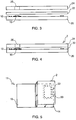
- the various layers constituting the RFID device support as shown on FIG. figure 3 consist of the antenna support 20, a thermoplastic layer 22 and an upper layer 24
- the device is made by lamination of the various layers once the chip is fixed on the antenna support 20.
- a first thermoplastic layer 22 is disposed on the antenna support 20.
- the thickness of the thermoplastic layer is included between 40 and 80 microns and is preferably of the order of 50 microns.
- the upper layer 24 has a cavity 26 located so as to be superimposed on the chip and whose area is greater than that of the chip so that the pressure exerted during the lamination step does not reach the chip because the pressure occurs evenly over the entire surface of the leaf but does not occur at the location of the cavity above the location of the chip;
- the cavity 26 is preferably circular with a diameter of the order of 6 mm.
- the lamination step comprises heat-sealing the layers 20, 22, 24 to obtain an RFID device holder 2 as shown in FIG. figure 4 .
- the temperature and the pressure reached are respectively of the order of 160 ° C. and 200 bars.
- the antenna support 20 is preferably in a material that does not flow so that does not deform irreversibly when the temperature increases. up to 160 ° C. In addition, this material does not delaminate voluntarily or involuntarily over time.
- the support 20 is preferably a synthetic paper consisting of a single unoriented layer of a polymer such as polyethylene or polypropylene loaded with mineral fillers between 40 and 80%.
- thermoplastic layer 22 directly in contact with the chip, is not pierced with a cavity at the location of the chip, the pressure exerted during the lamination is not transmitted to the chip at the point of the chip. 'to damage.
- the thermoplastic component of the layer 22 softens and fluidifies while being trapped between the two respective layers of the antenna support 20 and the top layer 24.
- the antenna support gives the device composed of the antenna 10 and the chip 12 a rigidity and a cohesion that prevents electrical breakage since the material of the layer forming the antenna support resists without deformation and especially without flow at the temperatures and pressures of the lamination step.
- the stiffened thermoplastic layer 22 has trapped the reliefs of the antenna support 20 so that the antenna 10 and the chip 12 are embedded in the thermoplastic 22.
- thermoplastic layer which gives the RFID device carrier rigidity and cohesion that prevents electrical breakage.
- Thermoplastic can weld together the two layers 20 and 24 and plays the role of glue between these two layers.
- the upper layer 24 with a thickness of 180 ⁇ m is preferably in the same material as the antenna support 20 and therefore in synthetic paper as defined above.
- the support of the RFID device 2 thus produced by lamination of the layers 20, 22, 24 and shown in section on the figure 3 has a thickness of about 350 ⁇ m.
- the flexibility and flexibility of the RFID device support 2 obtained is a function of the thickness of the thermoplastic layer 22 used. The smaller the thickness of the thermoplastic layer, the more flexible and flexible the RFID device.
- the support of the RFID device 2 is stuck on one of the two plates of the cover 11 of the identity booklet, preferably on the lower plate 14 but could also be glued to the top plate 16.
- the RFID device holder 2 is glued using an adhesive which, once dry, is insoluble in water.
- the support 3 is therefore preferably of identical size to the device support 2.
- a support 3 without an RFID device consisting of a single layer of synthetic paper 50 or else laminating together a layer of synthetic paper, a layer of thermoplastic and a layer of synthetic paper, the single layer or all the layers being of the same total thickness as all the layers 20, 22 and 24.
- the support 3 thus manufactured is then stuck on the second flat cover 11 of the booklet, while leaving a free band of the cover at the location of the hinge of the booklet.
- the supports 2 and 3 are manufactured together so as to be secured to one another by a single upper layer of synthetic paper 64 as shown in FIG. figure 7 by a support device RFID device 4.
- a first layer of thermoplastic 22 is disposed on the antenna support 20 whose thickness is between 40 and 80 microns but preferably of the order of 50 microns.
- a second thermoplastic layer 62 is also disposed on a second layer 60 of synthetic paper.
- the layers 20, 22, 60 and 62 having the same size corresponding in length to the size of a closed identity booklet but whose width is slightly less than the width of a closed identity booklet.
- An upper layer 64 is disposed on the layers 22 and 62 so as to leave a space between them.
- the layer 64 has a cavity 26 located so as to be superimposed on the chip and whose area is greater than that of the chip so that the pressure exerted during the lamination step does not reach the chip because the pressure s exerts uniformly over the entire surface of the leaf but does not exert at the location of the cavity placed above the location of the chip;
- the cavity 26 is preferably circular with a diameter of the order of 6 mm.
- the support 4 serving as an RFID device support for the embodiment of the invention is shown in section on the figure 8 .
- the size of the booklet open ID it comprises two thick parts 42 and 43, the portion 42 containing the RFID device, the two parts being superimposed on the plates 14 and 16 of the cover 11 of the booklet and a less thick part intended to be superimposed on the hinge of the identity booklet.
- the RFID device holder 2 as described can also be integrated into the booklet by gluing one of its faces, but preferably on the side of the antenna support, on any type of object such as clothing, books, documents. paper, packaging, cartons, etc.
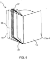
- the identity booklet 1 schematically represented on the figure 9 is completely formed by the setting up of the notebook of the inner pages 37.
- the method of confection consists of elaborating the notebook of the inner pages by using a secure thread to connect them between them.
- the cover sheets are laminated on the cover plates, the cover page 36 being laminated to the upper plate 16 while the lower cover page 34 is laminated to the lower plate 14.
- the back of the lower cover page 34 of the pages book of the identity book is glued and then pressed against the RFID device holder 2 glued to the lower plate 14 of the cover of the booklet, therefore on the side of the layer of the antenna support 20.
- the back of the lower cover page 34 of the booklet of the pages of the booklet identity is glued and then pressed against the portion 42 of the support 4, the portion 42 being the one containing the chip and the antenna while the front of the cover page 36 is glued and then pressed against the portion 43 of the support 4.
- the glue used is preferably an adhesive which, once dried becomes insoluble in water.
- the synthetic paper facilitates the lamination operation carried out at temperatures of the order of 160 ° C, since it is stable at these temperatures unlike thermoplastic materials such as PVC or PETG.
- the support of the RFID device 2 or 4 made according to the invention has synthetic paper on both sides, which facilitates its bonding and optimizes its integration in the identity booklet since the collages are made paper against synthetic paper.
- synthetic paper has a low density due to its microporous structure, which gives it a good bonding affinity with paper unlike conventional plastics such as PVC or PET.
- the identity booklet thus obtained provides the advantage of a great cohesion between all the parts that compose it and in particular between the RFID device holder and the identity booklet itself.
- the glue penetrates deep into the thickness of the synthetic paper as it enters the paper and therefore in particular in the paper making up the cover of the booklet, which makes it impossible to separate the layers 20, 22 and 24 between them and which makes the three constituent layers of the support indissociable.
- the thermoplastic used for the layers 22 and 52 is preferably polyvinyl chloride (PVC), but can also be polyester (PET, PETG), polypropylene (PP), polycarbonate (PC) or acrylonitrile-butadiene- styrene (ABS).
- PVC polyvinyl chloride
- PETG PETG
- PP polypropylene
- PC polycarbonate
- ABS acrylonitrile-butadiene- styrene
- the outside of the cover of the booklet may be subject to a plate having particular reliefs so as to produce a particular grain on the cover and so as to make the identity booklet unfalsifiable.
- the RFID device holder and the identity booklet according to the invention can pass through a washing machine without the electrical connection between the chip and the antenna being altered thus keeping the possibility of being read by electromagnetic coupling with a reader provided for this purpose.
- the RFID device support and the RFID device can also be made in ISO format of the smart cards so as to be used for the manufacture of contactless smart card.
- the two outer synthetic paper layers and the thermoplastic layer are in ISO format of smart cards and the antenna is also adapted so that the size of the turns are slightly smaller than the ISO format of the smart cards.
- an additional step to the manufacturing method described above is to customize the card by printing on one side of the card or both.
Landscapes
- Engineering & Computer Science (AREA)
- Physics & Mathematics (AREA)
- General Physics & Mathematics (AREA)
- Theoretical Computer Science (AREA)
- Computer Hardware Design (AREA)
- Microelectronics & Electronic Packaging (AREA)
- Credit Cards Or The Like (AREA)
- Details Of Aerials (AREA)
- Input Circuits Of Receivers And Coupling Of Receivers And Audio Equipment (AREA)
- Superheterodyne Receivers (AREA)
- Support Of Aerials (AREA)
Claims (11)
- Träger einer Hochfrequenz-Identifikationsvorrichtung (4), die eine Antenne (12), die durch Siebdruck auf einen Antennenträger (20) aufgebracht wird, und einen Chip (10) enthält, der mit den Anschlussklemmen (17 und 19) der Antenne verbunden ist, wobei der Träger ebenfalls eine erste Thermoplastschicht (22), die auf den Antennenträger (20) laminiert wird, eine zweite Thermoplastschicht (62), die auf eine Schicht (60) aus synthetischem Papier laminiert wird, und eine obere Schicht (64) aus synthetischem Papier enthält, die so auf die Thermoplastschichten (22 und 62) laminiert wird, dass ein Zwischenraum zwischen den Thermoplastschichten freigelassen wird, wobei der erhaltene Träger zwei dicke Teile (42, 43) enthält, wobei ein dicker Teil (42) die RFID-Vorrichtung enthält.
- Träger einer RFID-Vorrichtung (4) nach Anspruch 1, bei dem die obere Schicht (64) einen Hohlraum (26) enthält, der so angeordnet ist, dass er den Chip (10) überlagert.
- Träger einer RFID-Vorrichtung (4) nach Anspruch 1 oder 2, bei dem der Chip (10) mit Hilfe eines haftenden Dielektrikums so auf den Antennenträger (20) geklebt wird, dass die Anschlusskontakte des Chips sich gegenüber den Anschlusskontakten (17 und 19) der Antenne (12) befinden.
- Träger einer RFID-Vorrichtung (4) nach Anspruch 3, bei dem das haftende Material ein Expoxidharz ist, das bei 150°C vernetzt.
- Träger einer RFID-Vorrichtung (4) nach einem der vorhergehenden Ansprüche, bei dem die Laminierung bei Temperatur- und Druckwerten in der Größenordnung von 160°C und 200 Bar durchgeführt wird.
- Träger einer RFID-Vorrichtung (4) nach einem der Ansprüche 1 bis 5, bei dem das synthetische Papier der oberen Schicht (64) aus einem nicht kriechenden Material besteht, d.h. das sich bei steigender Temperatur nicht verformt.
- Träger einer RFID-Vorrichtung (4) nach einem der vorhergehenden Ansprüche, bei dem die erste Thermoplastschicht (22) eine Dicke von 50 µm hat.
- Personenstandsbuch (1), das einen Träger einer RFID-Vorrichtung (4) nach einem der Ansprüche 1 bis 7 enthält, wobei der Träger der RFID-Vorrichtung (4) die Größe des offenen Personenstandsbuchs zwischen den zwei dicken Teilen (42, 43) hat, die die Deckel (14 und 16) des Einbands (11) des Buchs überlagern, wobei der Träger (4) ebenfalls einen weniger dicken Teil aufweist, der dazu bestimmt ist, den Ansatzfalz des Personenstandsbuchs zu überlagern.
- Personenstandsbuch nach Anspruch 8, bei dem der Träger der RFID-Vorrichtung (4) ins Innere des Personenstandsbuchs (1) mit Hilfe eines Klebstoffs geklebt wird, der, wenn er trocken ist, wasserunlöslich ist.
- Verfahren zur Herstellung eines Trägers einer Hochfrequenz-Identifikationsvorrichtung (4), wobei die Vorrichtung eine Antenne und einen mit der Antenne verbundenen Chip enthält, wobei das Verfahren die folgenden Schritte enthält:- Siebdrucken einer Anschlusskontakte (17 und 19) aufweisenden Antenne (12) auf einen Antennenträger (20),- Aufbringen eines haftenden Dielektrikums zwischen den Anschlusskontakten der Antenne,- Positionieren des Chips (10) auf dem Antennenträger (20) derart, dass die Anschlüsse des Chips sich gegenüber den Anschlusskontakten der Antenne befinden,- Verbinden des Chips mit den Anschlusskontakten der Antenne durch Ausüben eines Drucks auf den Chip,- Aufbringen einer ersten Thermoplastschicht (22) auf den Antennenträger,- Aufbringen einer zweiten Thermoplastschicht (62) auf eine Schicht (60) aus synthetischem Papier,- Aufbringen einer oberen Schicht eines nicht kriechenden Materials (64), wie eines synthetischen Papiers, auf die Schichten (22 und 62), wobei die obere Schicht (64) mit einem Hohlraum (26) an der Stelle des Chips (10) versehen ist,- Laminieren des Antennenträgers (20) mit den Thermoplastschichten (22 und 62), der Schicht aus synthetischem Papier (60) und der oberen Schicht (64), um eine aus zwei Teilen (42 und 43) gleicher Abmessung, wobei ein Teil (42) die RFID-Vorrichtung enthält, und einem weniger dicken Teil, der sich zwischen den zwei Teilen gleicher Abmessung (42 und 43) befindet, geformte RFID-Vorrichtung (4) zu erhalten.
- Verfahren zur Herstellung eines Personenstandsbuchs mit Hochfrequenz-Identifikationsvorrichtung (RFID) nach Anspruch 10, wobei die Vorrichtung (4) zwischen die Deckel (14 und 16) des Einbands des Buchs und die Vorsatzblätter (34 und 36) eingefügt ist, wobei das Verfahren nach dem Schritt des Laminierens die folgenden Schritte enthält:- Kleben des Trägers der RFID-Vorrichtung (4) auf die Deckel des Einbands des Personenstandsbuchs, indem die dem Antennenträger (20) entgegengesetzte Seite eingekleistert wird, so dass der am wenigsten dicke Teil des Trägers der RFID-Vorrichtung (4) den Ansatzfalz des Personenstandsbuchs überlagert,- Anordnen des Hefts der Innenseiten (37),- Kleben des Vorsatzblatts (34) gegen den Träger der RFID-Vorrichtung (4), hierzu wird die Rückseite des inneren Vorsatzblatts (34) des Hefts der Seiten des Personenstandsbuchs eingekleistert und dann gegen einen Teil (42) des Trägers (4) gedrückt, wobei der Teil (42) derjenige ist, der den Chip und die Antenne enthält, während die Vorderseite des Vorsatzblatts (36) eingekleistert und dann gegen den anderen (43) der zwei Teile des Trägers (4) gedrückt wird.
Applications Claiming Priority (3)
| Application Number | Priority Date | Filing Date | Title |
|---|---|---|---|
| FR0603862A FR2900485B3 (fr) | 2006-04-28 | 2006-04-28 | Support de dispositif d'identification radiofrequence et son procede de fabrication |
| FR0603860A FR2900484B3 (fr) | 2006-04-28 | 2006-04-28 | Support de dispositif d'identification radiofrequence et son procede de fabrication |
| PCT/FR2007/000735 WO2007125214A2 (fr) | 2006-04-28 | 2007-04-27 | Support de dispositif d'identification radiofrequence et son procede de fabrication |
Publications (2)
| Publication Number | Publication Date |
|---|---|
| EP2021985A2 EP2021985A2 (de) | 2009-02-11 |
| EP2021985B1 true EP2021985B1 (de) | 2012-04-18 |
Family
ID=38565460
Family Applications (1)
| Application Number | Title | Priority Date | Filing Date |
|---|---|---|---|
| EP07731387A Active EP2021985B1 (de) | 2006-04-28 | 2007-04-27 | Hochfrequenz-identifikationseinrichtungsmedium und herstellungsverfahren dafür |
Country Status (10)
| Country | Link |
|---|---|
| EP (1) | EP2021985B1 (de) |
| JP (1) | JP2009535874A (de) |
| KR (1) | KR101351904B1 (de) |
| AT (1) | ATE554461T1 (de) |
| BR (1) | BRPI0710714A2 (de) |
| CA (1) | CA2653409A1 (de) |
| IL (1) | IL195386A (de) |
| MX (1) | MX2008013611A (de) |
| TW (2) | TWI437498B (de) |
| WO (2) | WO2007125215A2 (de) |
Cited By (1)
| Publication number | Priority date | Publication date | Assignee | Title |
|---|---|---|---|---|
| EP4621641A1 (de) * | 2024-03-19 | 2025-09-24 | Giesecke+Devrient ePayments GmbH | Herstellen eines trägerkörpers für einen portablen datenträger |
Family Cites Families (20)
| Publication number | Priority date | Publication date | Assignee | Title |
|---|---|---|---|---|
| US5528222A (en) * | 1994-09-09 | 1996-06-18 | International Business Machines Corporation | Radio frequency circuit and memory in thin flexible package |
| GB2294899B (en) * | 1994-11-11 | 1997-08-27 | Plessey Telecomm | Method of manufacturing a smartcard |
| US5786626A (en) * | 1996-03-25 | 1998-07-28 | Ibm Corporation | Thin radio frequency transponder with leadframe antenna structure |
| DE69819299T2 (de) * | 1997-06-23 | 2004-07-29 | Rohm Co. Ltd. | Ic modul und ic karte |
| JP2000048162A (ja) * | 1998-03-17 | 2000-02-18 | Sanyo Electric Co Ltd | Icカード用モジュール、icカード用モジュールの製造方法、混成集積回路モジュールおよびその製造方法 |
| JPH11345298A (ja) * | 1998-06-02 | 1999-12-14 | Toppan Printing Co Ltd | 非接触型icカード及びその製造方法 |
| JP2000080594A (ja) * | 1998-09-02 | 2000-03-21 | Toppan Printing Co Ltd | ポリシランコーティング紙 |
| US6262692B1 (en) * | 1999-01-13 | 2001-07-17 | Brady Worldwide, Inc. | Laminate RFID label and method of manufacture |
| US6147662A (en) | 1999-09-10 | 2000-11-14 | Moore North America, Inc. | Radio frequency identification tags and labels |
| US6951596B2 (en) * | 2002-01-18 | 2005-10-04 | Avery Dennison Corporation | RFID label technique |
| FR2824018B1 (fr) * | 2001-04-26 | 2003-07-04 | Arjo Wiggins Sa | Couverture incorporant un dispositif d'identification radiofrequence |
| JP4843865B2 (ja) * | 2001-04-27 | 2011-12-21 | 凸版印刷株式会社 | 蓋材 |
| JP4830237B2 (ja) * | 2001-08-27 | 2011-12-07 | 凸版印刷株式会社 | 非接触icカード記録媒体及びその製造方法 |
| JP4471971B2 (ja) * | 2003-03-12 | 2010-06-02 | ブンデスドゥルッケレイ・ゲーエムベーハー | ブックカバーインサートとブック型セキュリティ文書、及びブックカバーインサートとブック型セキュリティ文書の製造方法 |
| FR2853115B1 (fr) * | 2003-03-28 | 2005-05-06 | A S K | Procede de fabrication d'antenne de carte a puce sur un support thermoplastique et carte a puce obtenue par ledit procede |
| JP2005170958A (ja) * | 2003-11-17 | 2005-06-30 | Dai Ichi Kogyo Seiyaku Co Ltd | カチオン電着塗料組成物及びカチオン電着塗装方法 |
| JP2005229098A (ja) * | 2003-12-12 | 2005-08-25 | Semiconductor Energy Lab Co Ltd | 半導体装置及び半導体装置の作製方法 |
| DE102004008840A1 (de) * | 2004-02-20 | 2005-09-01 | Bundesdruckerei Gmbh | Verfahren zur Herstellung eines buchartigen Wertdokuments sowie ein buchartiges Wertdokument |
| FR2881252A1 (fr) * | 2005-01-24 | 2006-07-28 | Ask Sa | Dispositif d'idenfication radiofrequence resistant aux milieux et son procede de fabrication |
| CN101087453A (zh) * | 2006-06-05 | 2007-12-12 | 美国通宝科技股份有限公司 | 用户识别模组卡及其与射频识别天线的组合 |
-
2007
- 2007-04-27 BR BRPI0710714-5A patent/BRPI0710714A2/pt not_active IP Right Cessation
- 2007-04-27 AT AT07731387T patent/ATE554461T1/de active
- 2007-04-27 WO PCT/FR2007/000736 patent/WO2007125215A2/fr not_active Ceased
- 2007-04-27 JP JP2009507120A patent/JP2009535874A/ja active Pending
- 2007-04-27 MX MX2008013611A patent/MX2008013611A/es active IP Right Grant
- 2007-04-27 WO PCT/FR2007/000735 patent/WO2007125214A2/fr not_active Ceased
- 2007-04-27 KR KR1020087026348A patent/KR101351904B1/ko active Active
- 2007-04-27 EP EP07731387A patent/EP2021985B1/de active Active
- 2007-04-27 CA CA002653409A patent/CA2653409A1/fr not_active Abandoned
- 2007-04-30 TW TW096115284A patent/TWI437498B/zh active
- 2007-04-30 TW TW096115289A patent/TWI447651B/zh active
-
2008
- 2008-11-19 IL IL195386A patent/IL195386A/en active IP Right Grant
Cited By (1)
| Publication number | Priority date | Publication date | Assignee | Title |
|---|---|---|---|---|
| EP4621641A1 (de) * | 2024-03-19 | 2025-09-24 | Giesecke+Devrient ePayments GmbH | Herstellen eines trägerkörpers für einen portablen datenträger |
Also Published As
| Publication number | Publication date |
|---|---|
| WO2007125215A3 (fr) | 2008-01-10 |
| TWI447651B (zh) | 2014-08-01 |
| TW200842724A (en) | 2008-11-01 |
| MX2008013611A (es) | 2008-11-10 |
| IL195386A0 (en) | 2011-08-01 |
| KR20080111108A (ko) | 2008-12-22 |
| KR101351904B1 (ko) | 2014-01-23 |
| TW200842723A (en) | 2008-11-01 |
| CA2653409A1 (fr) | 2007-11-08 |
| WO2007125214A3 (fr) | 2008-01-03 |
| ATE554461T1 (de) | 2012-05-15 |
| BRPI0710714A2 (pt) | 2011-08-23 |
| EP2021985A2 (de) | 2009-02-11 |
| IL195386A (en) | 2013-11-28 |
| HK1134959A1 (en) | 2010-05-20 |
| WO2007125215A2 (fr) | 2007-11-08 |
| TWI437498B (zh) | 2014-05-11 |
| WO2007125214A2 (fr) | 2007-11-08 |
| JP2009535874A (ja) | 2009-10-01 |
Similar Documents
| Publication | Publication Date | Title |
|---|---|---|
| EP2203875B1 (de) | Einbanddeckel für einen reisepass mit funkfrequenzidentifizierungsvorrichtung und hestellungsverfahren dafür | |
| EP1183644B1 (de) | Verfahren zur herstellung einer kontaktlosen hybriden chipkarte mit einem antennenträger aus fasermaterial | |
| WO2006077339A1 (fr) | Dispositif d'identification radiofrequence resistant aux milieux humides et son procede de fabrication | |
| EP1442424B1 (de) | Verfahren zur herstellung einer kontaktlosen chipkarte oder einer hybriden chipkarte mit und ohne kontakten mit verbesserter flachheit | |
| EP1183643B1 (de) | Verfahren zur herstellung einer kontaktlosen chipkarte mit einem antennenträger aus fasermaterial | |
| EP1745419B1 (de) | Struktur mit einer elektronischen einrichtung insbesondere zur herstellung eines sicherheit- oder wertdokuments | |
| EP1609117B1 (de) | Verfahren zur herstellung einer chipkarten-antenne auf einem thermoplastischen träger und einer danach hergestellten chipkarte | |
| FR2900484A1 (fr) | Support de dispositif d'identification radiofrequence et son procede de fabrication | |
| FR2948796A1 (fr) | Support de dispositif d'identification radiofrequence pour carte hybride et son procede de fabrication | |
| FR2782821A1 (fr) | Procede de fabrication de carte a puce sans contact | |
| FR2900485A1 (fr) | Support de dispositif d'identification radiofrequence et son procede de fabrication | |
| WO2018104482A1 (fr) | Assemblage securise de document ou de support | |
| EP2021985A2 (de) | Hochfrequenz-identifikationseinrichtungsmedium und herstellungsverfahren dafür | |
| FR2881251A1 (fr) | Livret d'identite a dispositif d'identification radiofrequence resistant aux milieux humides | |
| WO2004084130A1 (fr) | Procede de fabrication d’une carte a puce sans contact a planeite renforcee | |
| HK1134959B (en) | Radio frequency identification device medium and method for making same |
Legal Events
| Date | Code | Title | Description |
|---|---|---|---|
| PUAI | Public reference made under article 153(3) epc to a published international application that has entered the european phase |
Free format text: ORIGINAL CODE: 0009012 |
|
| 17P | Request for examination filed |
Effective date: 20081125 |
|
| AK | Designated contracting states |
Kind code of ref document: A2 Designated state(s): AT BE BG CH CY CZ DE DK EE ES FI FR GB GR HU IE IS IT LI LT LU LV MC MT NL PL PT RO SE SI SK TR |
|
| AX | Request for extension of the european patent |
Extension state: AL BA HR MK RS |
|
| DAX | Request for extension of the european patent (deleted) | ||
| 17Q | First examination report despatched |
Effective date: 20110215 |
|
| GRAP | Despatch of communication of intention to grant a patent |
Free format text: ORIGINAL CODE: EPIDOSNIGR1 |
|
| GRAS | Grant fee paid |
Free format text: ORIGINAL CODE: EPIDOSNIGR3 |
|
| GRAA | (expected) grant |
Free format text: ORIGINAL CODE: 0009210 |
|
| AK | Designated contracting states |
Kind code of ref document: B1 Designated state(s): AT BE BG CH CY CZ DE DK EE ES FI FR GB GR HU IE IS IT LI LT LU LV MC MT NL PL PT RO SE SI SK TR |
|
| REG | Reference to a national code |
Ref country code: GB Ref legal event code: FG4D Free format text: NOT ENGLISH |
|
| REG | Reference to a national code |
Ref country code: CH Ref legal event code: EP |
|
| REG | Reference to a national code |
Ref country code: IE Ref legal event code: FG4D Free format text: LANGUAGE OF EP DOCUMENT: FRENCH |
|
| REG | Reference to a national code |
Ref country code: AT Ref legal event code: REF Ref document number: 554461 Country of ref document: AT Kind code of ref document: T Effective date: 20120515 |
|
| REG | Reference to a national code |
Ref country code: DE Ref legal event code: R096 Ref document number: 602007022097 Country of ref document: DE Effective date: 20120621 |
|
| REG | Reference to a national code |
Ref country code: NL Ref legal event code: VDEP Effective date: 20120418 |
|
| REG | Reference to a national code |
Ref country code: AT Ref legal event code: MK05 Ref document number: 554461 Country of ref document: AT Kind code of ref document: T Effective date: 20120418 |
|
| LTIE | Lt: invalidation of european patent or patent extension |
Effective date: 20120418 |
|
| BERE | Be: lapsed |
Owner name: ASK S.A. Effective date: 20120430 |
|
| PG25 | Lapsed in a contracting state [announced via postgrant information from national office to epo] |
Ref country code: IS Free format text: LAPSE BECAUSE OF FAILURE TO SUBMIT A TRANSLATION OF THE DESCRIPTION OR TO PAY THE FEE WITHIN THE PRESCRIBED TIME-LIMIT Effective date: 20120818 Ref country code: SE Free format text: LAPSE BECAUSE OF FAILURE TO SUBMIT A TRANSLATION OF THE DESCRIPTION OR TO PAY THE FEE WITHIN THE PRESCRIBED TIME-LIMIT Effective date: 20120418 Ref country code: CY Free format text: LAPSE BECAUSE OF FAILURE TO SUBMIT A TRANSLATION OF THE DESCRIPTION OR TO PAY THE FEE WITHIN THE PRESCRIBED TIME-LIMIT Effective date: 20120418 Ref country code: FI Free format text: LAPSE BECAUSE OF FAILURE TO SUBMIT A TRANSLATION OF THE DESCRIPTION OR TO PAY THE FEE WITHIN THE PRESCRIBED TIME-LIMIT Effective date: 20120418 Ref country code: LT Free format text: LAPSE BECAUSE OF FAILURE TO SUBMIT A TRANSLATION OF THE DESCRIPTION OR TO PAY THE FEE WITHIN THE PRESCRIBED TIME-LIMIT Effective date: 20120418 Ref country code: PL Free format text: LAPSE BECAUSE OF FAILURE TO SUBMIT A TRANSLATION OF THE DESCRIPTION OR TO PAY THE FEE WITHIN THE PRESCRIBED TIME-LIMIT Effective date: 20120418 |
|
| PG25 | Lapsed in a contracting state [announced via postgrant information from national office to epo] |
Ref country code: PT Free format text: LAPSE BECAUSE OF FAILURE TO SUBMIT A TRANSLATION OF THE DESCRIPTION OR TO PAY THE FEE WITHIN THE PRESCRIBED TIME-LIMIT Effective date: 20120820 Ref country code: SI Free format text: LAPSE BECAUSE OF FAILURE TO SUBMIT A TRANSLATION OF THE DESCRIPTION OR TO PAY THE FEE WITHIN THE PRESCRIBED TIME-LIMIT Effective date: 20120418 Ref country code: LV Free format text: LAPSE BECAUSE OF FAILURE TO SUBMIT A TRANSLATION OF THE DESCRIPTION OR TO PAY THE FEE WITHIN THE PRESCRIBED TIME-LIMIT Effective date: 20120418 Ref country code: GR Free format text: LAPSE BECAUSE OF FAILURE TO SUBMIT A TRANSLATION OF THE DESCRIPTION OR TO PAY THE FEE WITHIN THE PRESCRIBED TIME-LIMIT Effective date: 20120719 Ref country code: MC Free format text: LAPSE BECAUSE OF NON-PAYMENT OF DUE FEES Effective date: 20120430 |
|
| REG | Reference to a national code |
Ref country code: CH Ref legal event code: PL |
|
| PG25 | Lapsed in a contracting state [announced via postgrant information from national office to epo] |
Ref country code: BE Free format text: LAPSE BECAUSE OF NON-PAYMENT OF DUE FEES Effective date: 20120430 Ref country code: LI Free format text: LAPSE BECAUSE OF NON-PAYMENT OF DUE FEES Effective date: 20120430 Ref country code: EE Free format text: LAPSE BECAUSE OF FAILURE TO SUBMIT A TRANSLATION OF THE DESCRIPTION OR TO PAY THE FEE WITHIN THE PRESCRIBED TIME-LIMIT Effective date: 20120418 Ref country code: DK Free format text: LAPSE BECAUSE OF FAILURE TO SUBMIT A TRANSLATION OF THE DESCRIPTION OR TO PAY THE FEE WITHIN THE PRESCRIBED TIME-LIMIT Effective date: 20120418 Ref country code: CH Free format text: LAPSE BECAUSE OF NON-PAYMENT OF DUE FEES Effective date: 20120430 Ref country code: SK Free format text: LAPSE BECAUSE OF FAILURE TO SUBMIT A TRANSLATION OF THE DESCRIPTION OR TO PAY THE FEE WITHIN THE PRESCRIBED TIME-LIMIT Effective date: 20120418 Ref country code: CZ Free format text: LAPSE BECAUSE OF FAILURE TO SUBMIT A TRANSLATION OF THE DESCRIPTION OR TO PAY THE FEE WITHIN THE PRESCRIBED TIME-LIMIT Effective date: 20120418 Ref country code: NL Free format text: LAPSE BECAUSE OF FAILURE TO SUBMIT A TRANSLATION OF THE DESCRIPTION OR TO PAY THE FEE WITHIN THE PRESCRIBED TIME-LIMIT Effective date: 20120418 Ref country code: RO Free format text: LAPSE BECAUSE OF FAILURE TO SUBMIT A TRANSLATION OF THE DESCRIPTION OR TO PAY THE FEE WITHIN THE PRESCRIBED TIME-LIMIT Effective date: 20120418 Ref country code: AT Free format text: LAPSE BECAUSE OF FAILURE TO SUBMIT A TRANSLATION OF THE DESCRIPTION OR TO PAY THE FEE WITHIN THE PRESCRIBED TIME-LIMIT Effective date: 20120418 |
|
| PLBE | No opposition filed within time limit |
Free format text: ORIGINAL CODE: 0009261 |
|
| STAA | Information on the status of an ep patent application or granted ep patent |
Free format text: STATUS: NO OPPOSITION FILED WITHIN TIME LIMIT |
|
| PG25 | Lapsed in a contracting state [announced via postgrant information from national office to epo] |
Ref country code: IT Free format text: LAPSE BECAUSE OF FAILURE TO SUBMIT A TRANSLATION OF THE DESCRIPTION OR TO PAY THE FEE WITHIN THE PRESCRIBED TIME-LIMIT Effective date: 20120418 |
|
| 26N | No opposition filed |
Effective date: 20130121 |
|
| PG25 | Lapsed in a contracting state [announced via postgrant information from national office to epo] |
Ref country code: IE Free format text: LAPSE BECAUSE OF NON-PAYMENT OF DUE FEES Effective date: 20120427 Ref country code: ES Free format text: LAPSE BECAUSE OF FAILURE TO SUBMIT A TRANSLATION OF THE DESCRIPTION OR TO PAY THE FEE WITHIN THE PRESCRIBED TIME-LIMIT Effective date: 20120729 |
|
| REG | Reference to a national code |
Ref country code: DE Ref legal event code: R097 Ref document number: 602007022097 Country of ref document: DE Effective date: 20130121 |
|
| PG25 | Lapsed in a contracting state [announced via postgrant information from national office to epo] |
Ref country code: BG Free format text: LAPSE BECAUSE OF FAILURE TO SUBMIT A TRANSLATION OF THE DESCRIPTION OR TO PAY THE FEE WITHIN THE PRESCRIBED TIME-LIMIT Effective date: 20120718 Ref country code: MT Free format text: LAPSE BECAUSE OF FAILURE TO SUBMIT A TRANSLATION OF THE DESCRIPTION OR TO PAY THE FEE WITHIN THE PRESCRIBED TIME-LIMIT Effective date: 20120418 |
|
| PG25 | Lapsed in a contracting state [announced via postgrant information from national office to epo] |
Ref country code: TR Free format text: LAPSE BECAUSE OF FAILURE TO SUBMIT A TRANSLATION OF THE DESCRIPTION OR TO PAY THE FEE WITHIN THE PRESCRIBED TIME-LIMIT Effective date: 20120418 |
|
| PG25 | Lapsed in a contracting state [announced via postgrant information from national office to epo] |
Ref country code: LU Free format text: LAPSE BECAUSE OF NON-PAYMENT OF DUE FEES Effective date: 20120427 |
|
| PG25 | Lapsed in a contracting state [announced via postgrant information from national office to epo] |
Ref country code: HU Free format text: LAPSE BECAUSE OF FAILURE TO SUBMIT A TRANSLATION OF THE DESCRIPTION OR TO PAY THE FEE WITHIN THE PRESCRIBED TIME-LIMIT Effective date: 20070427 |
|
| REG | Reference to a national code |
Ref country code: FR Ref legal event code: PLFP Year of fee payment: 9 |
|
| PGFP | Annual fee paid to national office [announced via postgrant information from national office to epo] |
Ref country code: FR Payment date: 20150427 Year of fee payment: 9 |
|
| REG | Reference to a national code |
Ref country code: FR Ref legal event code: GC Effective date: 20151210 |
|
| REG | Reference to a national code |
Ref country code: FR Ref legal event code: ST Effective date: 20161230 |
|
| PG25 | Lapsed in a contracting state [announced via postgrant information from national office to epo] |
Ref country code: FR Free format text: LAPSE BECAUSE OF NON-PAYMENT OF DUE FEES Effective date: 20160502 |
|
| PGFP | Annual fee paid to national office [announced via postgrant information from national office to epo] |
Ref country code: GB Payment date: 20260430 Year of fee payment: 20 |
|
| PGFP | Annual fee paid to national office [announced via postgrant information from national office to epo] |
Ref country code: DE Payment date: 20260416 Year of fee payment: 20 |