EP2020805B1 - Tragbares elektronisches Gerät und Berührungsbildschirm davon - Google Patents
Tragbares elektronisches Gerät und Berührungsbildschirm davon Download PDFInfo
- Publication number
- EP2020805B1 EP2020805B1 EP08104040A EP08104040A EP2020805B1 EP 2020805 B1 EP2020805 B1 EP 2020805B1 EP 08104040 A EP08104040 A EP 08104040A EP 08104040 A EP08104040 A EP 08104040A EP 2020805 B1 EP2020805 B1 EP 2020805B1
- Authority
- EP
- European Patent Office
- Prior art keywords
- transparent conductive
- conductive layer
- touch panel
- printed circuit
- flexible printed
- Prior art date
- Legal status (The legal status is an assumption and is not a legal conclusion. Google has not performed a legal analysis and makes no representation as to the accuracy of the status listed.)
- Not-in-force
Links
Images


Classifications
-
- H—ELECTRICITY
- H04—ELECTRIC COMMUNICATION TECHNIQUE
- H04M—TELEPHONIC COMMUNICATION
- H04M1/00—Substation equipment, e.g. for use by subscribers
- H04M1/02—Constructional features of telephone sets
- H04M1/23—Construction or mounting of dials or of equivalent devices; Means for facilitating the use thereof
-
- G—PHYSICS
- G06—COMPUTING OR CALCULATING; COUNTING
- G06F—ELECTRIC DIGITAL DATA PROCESSING
- G06F1/00—Details not covered by groups G06F3/00 - G06F13/00 and G06F21/00
- G06F1/16—Constructional details or arrangements
- G06F1/1613—Constructional details or arrangements for portable computers
- G06F1/1626—Constructional details or arrangements for portable computers with a single-body enclosure integrating a flat display, e.g. Personal Digital Assistants [PDAs]
-
- G—PHYSICS
- G06—COMPUTING OR CALCULATING; COUNTING
- G06F—ELECTRIC DIGITAL DATA PROCESSING
- G06F1/00—Details not covered by groups G06F3/00 - G06F13/00 and G06F21/00
- G06F1/16—Constructional details or arrangements
- G06F1/1613—Constructional details or arrangements for portable computers
- G06F1/1633—Constructional details or arrangements of portable computers not specific to the type of enclosures covered by groups G06F1/1615 - G06F1/1626
- G06F1/1637—Details related to the display arrangement, including those related to the mounting of the display in the housing
- G06F1/1643—Details related to the display arrangement, including those related to the mounting of the display in the housing the display being associated to a digitizer, e.g. laptops that can be used as penpads
-
- G—PHYSICS
- G06—COMPUTING OR CALCULATING; COUNTING
- G06F—ELECTRIC DIGITAL DATA PROCESSING
- G06F1/00—Details not covered by groups G06F3/00 - G06F13/00 and G06F21/00
- G06F1/16—Constructional details or arrangements
- G06F1/1613—Constructional details or arrangements for portable computers
- G06F1/1633—Constructional details or arrangements of portable computers not specific to the type of enclosures covered by groups G06F1/1615 - G06F1/1626
- G06F1/1656—Details related to functional adaptations of the enclosure, e.g. to provide protection against EMI, shock, water, or to host detachable peripherals like a mouse or removable expansions units like PCMCIA cards, or to provide access to internal components for maintenance or to removable storage supports like CDs or DVDs, or to mechanically mount accessories
-
- H—ELECTRICITY
- H04—ELECTRIC COMMUNICATION TECHNIQUE
- H04M—TELEPHONIC COMMUNICATION
- H04M1/00—Substation equipment, e.g. for use by subscribers
- H04M1/02—Constructional features of telephone sets
- H04M1/0202—Portable telephone sets, e.g. cordless phones, mobile phones or bar type handsets
- H04M1/026—Details of the structure or mounting of specific components
- H04M1/0266—Details of the structure or mounting of specific components for a display module assembly
Definitions
- the present invention is related to an electronic apparatus, and more specifically, to a handheld electronic apparatus and the touch panel thereof.
- a traditional Personal Digital Assistant usually uses a touch panel as an input interface.
- PDA Personal Digital Assistant
- a touch panel as an input interface.
- wireless network technology progresses, traditional cellular phones using keys for input no longer meet the demand of users. Therefore, an advanced cellular phone with a touch panel as the interface was introduced recently, and provided a brand new communication feeling.
- FIG. 1 illustrates a cross-sectional view of a cellular phone with a traditional touch panel.
- a cellular phone with touch panel 10 comprises a touch panel 11, a front cover 12, a display panel 16 and a rear cover 18.
- the front cover 12 and the rear cover 18 are assembled to each other, and the touch panel 11 and the display panel 16 are disposed between the front cover 12 and the rear cover 18.
- the front cover 12 protrudes and covers the rim of the touch panel 11, and the display panel 16 is placed below the touch panel 11.
- the touch panel 11 comprises a touch panel body 111 and a flexible printed circuit (FPC) 14.
- the flexible printed circuit 14 connects the touch panel body 111 and a main circuit board (not shown) for signal transmission.
- the front cover 12 covers the flexible printed circuit 14 and some part of the touch panel body 111. As a result, the front cover 12 sticks out from the touch panel body 111.
- the user 15 is limited by the front cover 12 when operating the touch panel body 111.
- the border of the touch panel body 111 i.e., the area of the touch panel body 111 connected to the front cover 12
- the border tends to become dirty because it is not easily cleaned.
- US 2004/0041796 A1 discloses a handheld electronic apparatus according to the preamble If claim 1 and a touch panel according to the preamble of claim 12.
- a flexible printed circuit used for interconnecting the touch panel is bent such as to embrace an outer rim of the touch panel.
- the flexible printed circuit is bent with a sharp angle, which uses to increased wear and a reduced lifetime of the flexible printed circuit board.
- a handheld electronic apparatus In a handheld electronic apparatus according to the present invention the front cover and the touch panel of the handheld electronic apparatus are assembled, so that the front cover will not stick out from the touch panel. Accordingly, the problem of the difficult operation of the touch panel border can be resolved, thereby providing the user a better operation feeling.
- the touch panel of the handheld electronic apparatus has a notch configured to accommodate one end of the flexible printed circuit connected to the touch panel body.
- the flexible printed circuit can extend in a curved manner through the notch. Therefore, the flexible printed circuit will not be bent perpendicularly or with a sharp angle, thereby increasing the lifetime of the flexible printed circuit.
- a handheld electronic apparatus comprises a front cover, a touch panel and a display panel.
- the front cover has a support portion with a first opening.
- the touch panel is placed on the support portion and covers the first opening.
- the touch panel comprises a touch panel body and a flexible printed circuit, in which the flexible printed circuit is connected to the touch panel body.
- the touch panel body comprises a first substrate, a first transparent conductive layer, a second transparent conductive layer, a second substrate and multiple spacers.
- the first substrate is placed on the support portion and covers the first opening, and the first substrate has a notch.
- the first transparent conductive layer is placed on the first substrate.
- the second transparent conductive layer is placed above the first transparent conductive layer.
- the second substrate is placed on the second transparent conductive layer.
- the spacers are placed between the first transparent conductive layer and the second transparent conductive layer.
- the flexible printed circuit has an end placed between the first transparent conductive layer and the second transparent conductive layer, and is electrically connected to the first transparent conductive layer and the second transparent conductive layer.
- the flexible printed circuit extends in a curved manner, and a part of the flexible printed circuit is received in the notch.
- the display panel is placed below the touch panel body.
- the present invention provides a handheld electronic apparatus and the touch panel thereof to resolve the non-user-friendly operation problem at the border of the touch panel and to provide better operation feeling.
- the invention is described in detail below with reference to drawings.
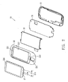
- FIG. 2 is an illustration of a handheld electronic apparatus 20 with separated components
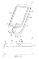
- FIG. 3 illustrates the handheld electronic apparatus 20 after assembly.
- the handheld electronic apparatus of the present invention may be a PDA, a cellular phone, a smart phone or other electronic apparatus having a touch panel.
- the handheld electronic apparatus 20 comprises a touch panel 21a, a front cover 22, a display panel 23, a main circuit board 24 and a rear cover 25.
- the front cover 22 comprises a support portion 221, and the support portion 221 has a first opening 222 and a second opening 223.
- the touch panel 21 a is placed on the support portion 221 and covers the first opening 222.
- the touch panel 21a comprises a touch panel body 210a and a flexible printed circuit 26, in which the border of the touch panel body 210a and the front cover 22 substantially form coplanar, and the flexible printed circuit 26 is connected to the touch panel body 210a.
- the flexible printed circuit 26 penetrates the second opening 223, and can be connected to the display panel 23 or directly connected to the main circuit board 24 as desired to transmit the signals inputted from the touch panel body 210a to the main circuit board 24 for signal processing.
- the first opening 222 and the second opening 223 can be connected.
- the front cover 22 has a third opening 224 adjacent to the second opening 223, and the third opening 224 is configured to expose a navigator key (not shown).
- the display panel 23 is placed below the touch panel body 210a.
- the rear cover 25 can be assembled with the front cover 22 to accommodate the display panel 23 and the main circuit board 24.
- the touch panel body 210a has a notch 27 at the bottom surface thereof to accommodate one end of the flexible printed circuit 26.
- the notch 27 is described in detail as follows with reference to the cross-sectional view shown in FIG. 4 .
- FIG. 4 is a cross-sectional view along line 1-1 of FIG. 3 .
- the front cover sticks out from the touch panel body, whereas for the present invention the front cover 22 and the touch panel body 210a of the handheld electronic apparatus 20 form coplanar after assembly, i.e., the front cover 22 and the border of the touch panel body 210a are substantially on the same level.
- the touch panel body 210a has a notch 27 at the bottom surface of one end thereof, so as to accommodate a portion of the flexible printed circuit 26 and allow the flexible printed circuit 26 to extend in a curved manner.
- the flexible printed circuit 26 is bent and connected to the display panel 23.
- the flexible printed circuit 26 can also be connected to the main circuit board 24 directly for signal transmission.
- the end of the touch panel body 210a connected to the flexible printed circuit 26 would substantially abut against the front cover 22 if there were no notch 27.
- the flexible printed circuit 26 would have to be perpendicularly bent downwards so as to be electrically in connection with the main circuit board 24, and as a consequence the lifetime of the flexible printed circuit 26 would be impacted.
- the notch 27 of the present invention in contrast, allows for a gently curved extension of the flexible printed circuit 26, thereby avoiding the lifetime reduction problem caused by the sharp bending of the flexible printed circuit 26.
- the details of the touch panel 21a are described below.
- FIG. 5 illustrates a cross-sectional view of a touch panel in accordance with a first embodiment of the present invention, which is a resistive touch panel of a film/glass type.
- the touch panel 21a is a multi-layer structure, and comprises a touch panel body 210a and a flexible printed circuit 26.
- the flexible printed circuit 26 is connected to the touch panel body 210a.
- the touch panel body 210a comprises a first substrate 211, a first transparent conductive layer 212, a plurality of spacers 213, an insulation layer 216, a second transparent conductive layer 214 and a second substrate 215.
- the first substrate 211 is placed on the support portion 221 and covers the first opening 222, and the first substrate 211 has a notch 27.
- the first transparent conductive layer 212 is placed on the first substrate 211.
- the second transparent conductive layer 214 is placed above the first transparent conductive layer 212, and is separated from the first transparent conductive layer 212 by the insulation layer 216 and the plurality of spacers 213.
- the insulation layer 216 is of a rectangle ring structure (as shown in FIG. 2 ) and surrounds the spacers 213.
- the second substrate 215 is disposed on the second transparent conductive layer 214.
- the first substrate 211 may be a plastic or glass substrate, whereas the second substrate 215 can be made of plastic such as poly (ethylene terephthalate) (PET) or the like. Moreover, when the first substrate 211 is a plastic substrate, the rigidity of the second substrate 215 is less than that of the first substrate 211.
- the first and second transparent conductive layers 212 and 214 may be selected from the group consisting of indium tin oxide (ITO), indium zinc oxide (IZO), aluminum doped zinc oxide (AZO), cadmium tin oxide (CTO), zinc oxide (ZnO) and zirconium dioxide (ZrO 2 ) or other transparent materials.
- the first transparent conductive layer 212 can be formed on the first substrate 211 by sputtering process
- the second transparent conductive layer 214 can be formed on the second substrate 215 by sputtering process also. If the first substrate 211 is a glass substrate, and the first transparent conductive layer 212 is made of ITO, those having ordinary knowledge in the art would refer to this bi-layer structure as an ITO glass.
- the second substrate 215 is made of PET and the second transparent conductive layer 214 is made of ITO, those having ordinary knowledge in the art would identify this bi-layer structure as an ITO film.
- the touch panel 21a of FIG. 5 can be called a resistive touch panel of a film/glass type.
- the first substrate 211 and the first transparent conductive layer 212 retract at one end and are connected to the flexible printed circuit 26.
- the first substrate 211 and the first transparent conductive layer 212 are shorter than the second transparent conductive layer 214 and the second substrate 215.
- One end of the flexible printed circuit 26 is placed between the first transparent conductive layer 212 and the second transparent conductive layer 214, and is electrically connected to the first transparent conductive layer 212 and the second transparent conductive layer 214.
- the flexible printed circuit 26 extends downwardly in a curved manner, and a part of the flexible printed circuit 26 is accommodated in the notch 27.
- the second transparent conductive layer 214 is placed above the notch 27, and the rim of the first substrate 211 and the rim of the first transparent conductive layer 212 at the notch 27 are aligned.
- the flexible printed circuit 26 in FIG. 5 is connected to the first transparent conductive layer 212, anyone having ordinary knowledge in the art can understand that the second transparent conductive layer 214 is connected to the flexible printed circuit 26 by soldering, applying conductive glue or other jump manners.
- FIG. 6 is a cross-sectional view of the touch panel in accordance with a second embodiment of the present invention, which is of the so-called film/film/glass type.
- the touch panel 21b comprises a touch panel body 210b and a flexible printed circuit 26.
- the flexible printed circuit 26 is connected to the touch panel body 210b.
- the touch panel body 210b comprises a first substrate 211, a glue layer 217, a third substrate 218, a first transparent conductive layer 212, an insulation layer 216, multiple spacers 213, a second transparent conductive layer 214 and a second substrate 215.
- the third substrate 218 is further formed between the first substrate 211 and the first transparent conductive layer 212, and the third substrate 218 is glued to the first substrate 211 by the glue layer 217.
- the bi-layer structure of the first transparent conductive layer 212 and the third substrate 218 is similar to the bi-layer structure of the second transparent conductive layer 214 and the second substrate 215.
- the third substrate 218 may be a plastic substrate, and can be made of PET or the like. If the third substrate 218 is made of PET and the first transparent conductive layer 212 is made of ITO, those having ordinary knowledge in the art would refer to this bi-layer structure as an ITO film.
- the ITO film is connected to the first substrate 211 by the glue layer 217. Consequently, the touch panel 21b of FIG. 6 is called a resistive touch panel of a film/film/glass type.
- a portion of the first substrate 211 and a portion of the first transparent conductive layer 212 shown in FIG. 5 are removed or stripped to form the notch 27, whereas the rims of the first substrate 211, the glue layer 217, the third substrate 218 and the first transparent conductive layer 212 shown in FIG. 6 are all removed at one time to form the notch 27.
- other methods can also be used to form the notch 27.
- a portion of the first substrate 211 can be removed to form the notch 27 first, and then the third substrate 218 and the first transparent conductive layer 212 are assembled to the first substrate 211 by the glue layer 217.
- the rim of the third substrate 218 and the rim of the first transparent conductive layer 212 are not aligned with the rim of the first substrate 211 at the notch 27. Accordingly, the third substrate 218 can cover a portion of the notch 27.
- the bending radius of the flexible printed circuit 26 may be between 0.2 and 1.5 mm, or the longitudinal depth along the extension direction of the flexible printed circuit 26 (i.e., the width "d" of the notch 27 shown in FIG. 5 and FIG. 6 ) may be between 0.2 and 1.5 mm.
- the notch 27 is not necessarily placed at the center of a side of the first substrate 211; other positions may be acceptable also.
- the first substrate of the touch panel has a notch; therefore if the touch panel is applied to a handheld electronic apparatus having flat upper surface, the extension of the flexible printed circuit will not be too-sharply bent which could decrease the lifetime.
Landscapes
- Engineering & Computer Science (AREA)
- Computer Hardware Design (AREA)
- Theoretical Computer Science (AREA)
- General Engineering & Computer Science (AREA)
- Human Computer Interaction (AREA)
- Physics & Mathematics (AREA)
- General Physics & Mathematics (AREA)
- Signal Processing (AREA)
- Position Input By Displaying (AREA)
- Telephone Set Structure (AREA)
- Push-Button Switches (AREA)
Claims (12)
- Tragbare elektronische Vorrichtung, umfassend:eine vordere Abdeckung (22) mit einem Halteabschnitt (221), wobei der Halteabschnitt eine erste Öffnung (222) aufweist;ein Berühungs-Eingabefeld (21a), das auf dem Halteabschnitt angeordnet ist und die erste Öffnung abdeckt, welches Berührungs-Eingabefeld umfasst:einen Berühungs-Eingabefeldkörper (210a; 210b), wobei der Berühungs-Eingabefeldkörper umfasst:einen ersten Träger (211), der auf dem Halteabschnitt (221) angeordnet ist und die erste Öffnung (222) abdeckt;eine erste transparente leitfähige Schicht (212), die auf dem ersten Träger angeordnet ist;eine zweite transparente leitfähige Schicht (214), die sich oberhalb der ersten transparenten leitfähigen Schicht befindet;einen zweiten Träger (215), der auf der zweiten transparenten leitfähigen Schicht (214) angeordnet ist;eine Mehrzahl von Abstandstücken (213), die zwischen der ersten transparenten leitfähigen Schicht und der zweiten transparenten leitfähigen Schicht angeordnet sind; undeine flexible gedruckte Leiterplatte (26), die mit dem Berühungs-Eingabefeldkörper (210a; 210b) verbunden ist, wobei ein Ende der flexiblen Leiterplatte zwischen der ersten transparenten leitfähigen Schicht (212) und der zweiten transparenten leitfähigen Schicht (214) angeordnet ist, die flexible Leiterplatte elektrisch leitend mit der ersten transparenten leitfähigen Schicht und mit der zweiten transparenten leitfähigen Schicht verbunden ist und die flexible Leiterplatte bogenförmig bzw. gewölbt ist; undein Anzeigefeld (23), das sich unterhalb des Berühungs-Eingabefeldkörpers befindet;dadurch gekennzeichnet, dass der erste Träger eine Einkerbung bzw. Aussparung (27) aufweist, wobei ein Abschnitt der flexiblen gedruckten Leiterplatte in der Einkerbung (27) aufgenommen ist.
- Tragbare elektronische Vorrichtung nach Anspruch 1, wobei sich ein Rand des Berühungs-Eingabefeldkörpers (210a; 210b) und der vorderen Abdeckung (22) im Wesentlichen auf dem gleichen Höhenniveau befinden.
- Tragbare elektronische Vorrichtung nach Anspruch 1 oder 2, wobei der Berühungs-Eingabefeldkörper (210a) außerdem eine Isolierungsschicht (216) aufweist, die sich zwischen der ersten transparenten leitfähigen Schicht (212) und der zweiten transparenten leitfähigen Schicht (214) befindet, und wobei die Isolierungsschicht die Mehrzahl von Abstandstücken umgibt bzw. einfasst.
- Tragbare elektronische Vorrichtung nach einem der vorhergehenden Ansprüche, wobei der Halteabschnitt (221) außerdem eine zweite Öffnung (223) aufweist und sich die flexible Leiterplatte durch die zweite Öffnung hindurch erstreckt.
- Tragbare elektronische Vorrichtung nach Anspruch 4, wobei die vordere Abdeckung (22) außerdem eine dritte Öffnung (224) aufweist, die an die zweite Öffnung (223) angrenzt, und wobei die dritte Öffnung ausgelegt ist, um einem Führungsschlüssel einen Zugang zu gewähren.
- Tragbare elektronische Vorrichtung nach einem der vorhergehenden Ansprüche, wobei der Berühungs-Eingabefeldkörper (219d) außerdem umfasst:eine Klebstoffschicht (217), die sich auf dem ersten Träger (211) belindet; undeinen dritten Träger (218), der sich zwischen der Klebstoffschicht und der ersten transparenten leitfähigen Schicht (212) befindet.
- Tragbare elektronische Vorrichtung nach einem der vorhergehenden Ansprüche, weiterhin umfassend eine Hauptleiterplatine (24), die elektrisch leitend mit dem anderen Ende der flexiblen Leiterplatte (26) verbunden ist.
- Tragbare elektronische Vorrichtung nach einem der vorhergehenden Ansprüche, weiterhin umfassend eine rückseitige Abdeckung (25), die mit der vorderen Abdeckung zusammengefügt ist, um das Anzeigefeld aufzunehmen.
- Tragbare elektronische Vorrichtung nach einem der vorhergehenden Ansprüche, wobei der erste Träger (211) ein Glas oder einen Kunststoff umfasst.
- Tragbare elektronische Vorrichtung nach einem der vorhergehenden Ansprüche, wobei die flexible Leiterplatte (26) einen Krümmungsradius zwischen 0,2 und 1,5 mm aufweist.
- Tragbare elektronische Vorrichtung nach einem der vorhergehenden Ansprüche, wobei die Einkerbung (27) eine Länge zwischen 0,2 und 1,5 mm entlang der Erstreckungsrichtung der flexiblen Leiterplatte (26) aufweist.
- Berührungs-Eingabefeld zur Verwendung in einer tragbaren elektronischen Vorrichtung nach einem der vorhergehenden Ansprüche, mit einem Berührungs-Eingabefeldkörper (210a; 210b), wobei der Berührungs-Eingabefeldkörper umfasst:einen ersten Träger (211), der auf dem Halteabschnitt (221) angeordnet ist und die erste Öffnung (222) abdeckt;eine erste transparente leitfähige Schicht (212), die sich auf dem ersten Träger befindet;eine zweite transparente leitfähige Schicht (214), die sich oberhalb der ersten transparenten leitfähigen Schicht befindet;einen zweiten Träger (215), der sich auf der zweiten transparenten leitfähigen Schicht (214) befindet;eine Mehrzahl von Abstandstücken (213), die zwischen der ersten transparenten leitfähigen Schicht und der zweiten transparenten leitfähigen Schicht angeordnet sind; undeine flexible Leiterplatte (269), die mit dem Berührungs-Eingabefeldkörper (210a; 210b) verbunden ist, wobei sich ein Ende der flexiblen Leiterplatte zwischen der ersten transparenten leitfähigen Schicht (212) und der zweiten transparenten leitfähigen Schicht (214) befindet, die flexible Leiterplatte elektrisch leitend mit der ersten transparenten leitfähigen Schicht und der zweiten transparenten leitfähigen Schicht verbunden ist und die flexible Leiterplatte gewölbt bzw. gekrümmt ist;dadurch gekennzeichnet, dass der erste Träger eine Einkerbung bzw. Aussparung (27) aufweist, wobei ein Abschnitt der flexiblen Leiterplatte in der Einkerbung bzw. Aussparung (27) aufgenommen ist.
Applications Claiming Priority (1)
| Application Number | Priority Date | Filing Date | Title |
|---|---|---|---|
| US95387607P | 2007-08-03 | 2007-08-03 |
Publications (2)
| Publication Number | Publication Date |
|---|---|
| EP2020805A1 EP2020805A1 (de) | 2009-02-04 |
| EP2020805B1 true EP2020805B1 (de) | 2010-09-15 |
Family
ID=39714077
Family Applications (1)
| Application Number | Title | Priority Date | Filing Date |
|---|---|---|---|
| EP08104040A Not-in-force EP2020805B1 (de) | 2007-08-03 | 2008-05-20 | Tragbares elektronisches Gerät und Berührungsbildschirm davon |
Country Status (7)
| Country | Link |
|---|---|
| US (1) | US8264467B2 (de) |
| EP (1) | EP2020805B1 (de) |
| JP (1) | JP2009038796A (de) |
| CN (1) | CN101360294A (de) |
| DE (1) | DE602008002501D1 (de) |
| ES (1) | ES2351101T3 (de) |
| TW (1) | TWI348636B (de) |
Families Citing this family (21)
| Publication number | Priority date | Publication date | Assignee | Title |
|---|---|---|---|---|
| USD957385S1 (en) | 2007-08-31 | 2022-07-12 | Apple Inc. | Electronic device |
| USD602015S1 (en) | 2008-04-07 | 2009-10-13 | Apple Inc. | Electronic device |
| TW201025088A (en) * | 2008-12-25 | 2010-07-01 | Chunghwa Picture Tubes Ltd | Touch panel structure with polarizer containing poly (ethylene terephthalate) |
| TWI448208B (zh) * | 2009-02-17 | 2014-08-01 | Pegatron Corp | 靜電防護元件及電子裝置 |
| CN101931665B (zh) * | 2009-06-25 | 2013-05-08 | 宏达国际电子股份有限公司 | 电子装置及其滑动机构 |
| FI122621B (fi) * | 2009-08-20 | 2012-04-30 | Lite On Mobile Oyj | Elektroniikkalaite ja sen kuoriosa |
| JP5886489B2 (ja) * | 2009-09-21 | 2016-03-16 | 株式会社ワコム | 位置検出装置 |
| JP2011107989A (ja) * | 2009-11-17 | 2011-06-02 | Fujitsu Ltd | 携帯機器 |
| KR101082162B1 (ko) * | 2009-12-03 | 2011-11-09 | 삼성모바일디스플레이주식회사 | 터치 스크린 패널 일체형 평판표시장치 |
| JP5871307B2 (ja) * | 2011-09-30 | 2016-03-01 | 株式会社ワコム | 位置検出センサユニットおよび位置検出装置 |
| JP5806599B2 (ja) * | 2011-11-21 | 2015-11-10 | アルプス電気株式会社 | 入力装置 |
| TWI475457B (zh) | 2012-09-03 | 2015-03-01 | Young Lighting Technology Inc | 觸控面板 |
| TW201421313A (zh) * | 2012-11-27 | 2014-06-01 | Young Lighting Technology Inc | 觸控裝置 |
| USD757699S1 (en) * | 2014-04-28 | 2016-05-31 | Samsung Electronics Co., Ltd. | Portable electronic device |
| CN104133592B (zh) * | 2014-07-30 | 2017-05-24 | 业成光电(深圳)有限公司 | 曲面触控装置 |
| CN104506673B (zh) * | 2014-08-06 | 2017-10-20 | 深圳市财富之舟科技有限公司 | 一种手机和手机的生产方法 |
| CN105988616A (zh) * | 2015-02-09 | 2016-10-05 | 宸鸿科技(厦门)有限公司 | 触控面板 |
| CN105100307B (zh) * | 2015-06-02 | 2018-04-06 | 青岛海信移动通信技术股份有限公司 | 一种移动终端芯片补强板的固定结构及移动终端 |
| CN108322572B (zh) * | 2018-03-21 | 2020-09-01 | 维沃移动通信有限公司 | 一种移动终端 |
| IT201900016313A1 (it) * | 2019-09-13 | 2021-03-13 | Martur Italy Srl | Pannello multistrato conduttivo per l’abitacolo di veicoli, in particolare autoveicoli |
| US12328811B2 (en) | 2021-07-27 | 2025-06-10 | Samsung Electronics Co., Ltd | Insulating member arrangement structure and electronic device including the same |
Family Cites Families (4)
| Publication number | Priority date | Publication date | Assignee | Title |
|---|---|---|---|---|
| JP2001102763A (ja) | 1999-09-30 | 2001-04-13 | Sanyo Electric Co Ltd | 携帯型入力装置 |
| JP4055311B2 (ja) | 1999-12-03 | 2008-03-05 | 株式会社デンソー | 携帯型情報端末 |
| KR100480154B1 (ko) | 2002-08-30 | 2005-04-06 | 엘지.필립스 엘시디 주식회사 | 터치패널 |
| JPWO2005064451A1 (ja) * | 2003-12-26 | 2007-12-20 | 日本写真印刷株式会社 | 保護パネル付き電子機器、保護パネル |
-
2007
- 2007-11-07 TW TW096141957A patent/TWI348636B/zh not_active IP Right Cessation
- 2007-11-13 CN CNA2007101664508A patent/CN101360294A/zh active Pending
-
2008
- 2008-05-13 US US12/119,767 patent/US8264467B2/en not_active Expired - Fee Related
- 2008-05-20 EP EP08104040A patent/EP2020805B1/de not_active Not-in-force
- 2008-05-20 DE DE602008002501T patent/DE602008002501D1/de active Active
- 2008-05-20 ES ES08104040T patent/ES2351101T3/es active Active
- 2008-07-09 JP JP2008178865A patent/JP2009038796A/ja active Pending
Also Published As
| Publication number | Publication date |
|---|---|
| US20090033634A1 (en) | 2009-02-05 |
| US8264467B2 (en) | 2012-09-11 |
| EP2020805A1 (de) | 2009-02-04 |
| ES2351101T3 (es) | 2011-01-31 |
| TWI348636B (en) | 2011-09-11 |
| TW200907769A (en) | 2009-02-16 |
| CN101360294A (zh) | 2009-02-04 |
| JP2009038796A (ja) | 2009-02-19 |
| DE602008002501D1 (de) | 2010-10-28 |
Similar Documents
| Publication | Publication Date | Title |
|---|---|---|
| US8264467B2 (en) | Handheld electronic apparatus and touch panel thereof | |
| US9836144B2 (en) | Touch panel | |
| EP2096525B1 (de) | Tragbares Endgerät | |
| US8212791B2 (en) | Protection panel with touch input function for display window of electronic device, and electronic device | |
| US8871541B2 (en) | Touch panel of an organic light emitting diode display and manufacturing method thereof | |
| EP2726964B1 (de) | Berührungsbildschirm und herstellungsverfahren dafür | |
| KR102342379B1 (ko) | 발광 장치 및 전자 기기 | |
| US20170285782A1 (en) | Touch panel and method of manufacturing the same | |
| US9841861B2 (en) | Touch panel with light-shielding layers | |
| US9667248B2 (en) | Touch panel | |
| US20140354591A1 (en) | Touch panel | |
| CN103186275A (zh) | 触控面板及其制作方法 | |
| US20150220184A1 (en) | Touch sensor | |
| CN107947779B (zh) | 触控按键结构、电子设备及一种触控按键结构制造方法 | |
| US20140293153A1 (en) | Touch panel and method for manufacturing the same | |
| US20130076667A1 (en) | Touch panel and a manufacturing method thereof | |
| US20110141036A1 (en) | Substrate for touch panel and touch panel | |
| US7026567B2 (en) | Touch panel | |
| KR20150092522A (ko) | 터치 패널 | |
| TW201504906A (zh) | 觸控式保護裝置 | |
| US8884172B2 (en) | Keypad apparatus for portable communication device | |
| US8228212B2 (en) | Touch-sensitive device | |
| US20150169098A1 (en) | Touch panel, touch display and manufacturing method of touch panel | |
| CN207367224U (zh) | 指纹辨识装置 | |
| US20110025617A1 (en) | Hybrid touch panel |
Legal Events
| Date | Code | Title | Description |
|---|---|---|---|
| PUAI | Public reference made under article 153(3) epc to a published international application that has entered the european phase |
Free format text: ORIGINAL CODE: 0009012 |
|
| 17P | Request for examination filed |
Effective date: 20080828 |
|
| AK | Designated contracting states |
Kind code of ref document: A1 Designated state(s): AT BE BG CH CY CZ DE DK EE ES FI FR GB GR HR HU IE IS IT LI LT LU LV MC MT NL NO PL PT RO SE SI SK TR |
|
| AX | Request for extension of the european patent |
Extension state: AL BA MK RS |
|
| AKX | Designation fees paid |
Designated state(s): DE ES FR GB IT NL |
|
| GRAP | Despatch of communication of intention to grant a patent |
Free format text: ORIGINAL CODE: EPIDOSNIGR1 |
|
| RAP1 | Party data changed (applicant data changed or rights of an application transferred) |
Owner name: HTC CORPORATION |
|
| GRAS | Grant fee paid |
Free format text: ORIGINAL CODE: EPIDOSNIGR3 |
|
| GRAA | (expected) grant |
Free format text: ORIGINAL CODE: 0009210 |
|
| AK | Designated contracting states |
Kind code of ref document: B1 Designated state(s): DE ES FR GB IT NL |
|
| REG | Reference to a national code |
Ref country code: GB Ref legal event code: FG4D |
|
| REF | Corresponds to: |
Ref document number: 602008002501 Country of ref document: DE Date of ref document: 20101028 Kind code of ref document: P |
|
| REG | Reference to a national code |
Ref country code: NL Ref legal event code: T3 |
|
| REG | Reference to a national code |
Ref country code: ES Ref legal event code: FG2A Effective date: 20110119 |
|
| PLBE | No opposition filed within time limit |
Free format text: ORIGINAL CODE: 0009261 |
|
| STAA | Information on the status of an ep patent application or granted ep patent |
Free format text: STATUS: NO OPPOSITION FILED WITHIN TIME LIMIT |
|
| 26N | No opposition filed |
Effective date: 20110616 |
|
| REG | Reference to a national code |
Ref country code: DE Ref legal event code: R097 Ref document number: 602008002501 Country of ref document: DE Effective date: 20110616 |
|
| REG | Reference to a national code |
Ref country code: FR Ref legal event code: PLFP Year of fee payment: 9 |
|
| REG | Reference to a national code |
Ref country code: FR Ref legal event code: PLFP Year of fee payment: 10 |
|
| REG | Reference to a national code |
Ref country code: FR Ref legal event code: PLFP Year of fee payment: 11 |
|
| PGFP | Annual fee paid to national office [announced via postgrant information from national office to epo] |
Ref country code: NL Payment date: 20190515 Year of fee payment: 12 |
|
| PGFP | Annual fee paid to national office [announced via postgrant information from national office to epo] |
Ref country code: ES Payment date: 20190603 Year of fee payment: 12 Ref country code: IT Payment date: 20190527 Year of fee payment: 12 Ref country code: DE Payment date: 20190508 Year of fee payment: 12 |
|
| PGFP | Annual fee paid to national office [announced via postgrant information from national office to epo] |
Ref country code: FR Payment date: 20190410 Year of fee payment: 12 |
|
| PGFP | Annual fee paid to national office [announced via postgrant information from national office to epo] |
Ref country code: GB Payment date: 20190515 Year of fee payment: 12 |
|
| REG | Reference to a national code |
Ref country code: DE Ref legal event code: R119 Ref document number: 602008002501 Country of ref document: DE |
|
| REG | Reference to a national code |
Ref country code: NL Ref legal event code: MM Effective date: 20200601 |
|
| PG25 | Lapsed in a contracting state [announced via postgrant information from national office to epo] |
Ref country code: NL Free format text: LAPSE BECAUSE OF NON-PAYMENT OF DUE FEES Effective date: 20200601 |
|
| GBPC | Gb: european patent ceased through non-payment of renewal fee |
Effective date: 20200520 |
|
| PG25 | Lapsed in a contracting state [announced via postgrant information from national office to epo] |
Ref country code: FR Free format text: LAPSE BECAUSE OF NON-PAYMENT OF DUE FEES Effective date: 20200531 Ref country code: GB Free format text: LAPSE BECAUSE OF NON-PAYMENT OF DUE FEES Effective date: 20200520 |
|
| PG25 | Lapsed in a contracting state [announced via postgrant information from national office to epo] |
Ref country code: DE Free format text: LAPSE BECAUSE OF NON-PAYMENT OF DUE FEES Effective date: 20201201 |
|
| REG | Reference to a national code |
Ref country code: ES Ref legal event code: FD2A Effective date: 20211004 |
|
| PG25 | Lapsed in a contracting state [announced via postgrant information from national office to epo] |
Ref country code: IT Free format text: LAPSE BECAUSE OF NON-PAYMENT OF DUE FEES Effective date: 20200520 |
|
| PG25 | Lapsed in a contracting state [announced via postgrant information from national office to epo] |
Ref country code: ES Free format text: LAPSE BECAUSE OF NON-PAYMENT OF DUE FEES Effective date: 20200521 |