EP2020691A2 - Lichtemittierende III-Nitrid-Halbleiter-Vorrichtung - Google Patents
Lichtemittierende III-Nitrid-Halbleiter-Vorrichtung Download PDFInfo
- Publication number
- EP2020691A2 EP2020691A2 EP08161500A EP08161500A EP2020691A2 EP 2020691 A2 EP2020691 A2 EP 2020691A2 EP 08161500 A EP08161500 A EP 08161500A EP 08161500 A EP08161500 A EP 08161500A EP 2020691 A2 EP2020691 A2 EP 2020691A2
- Authority
- EP
- European Patent Office
- Prior art keywords
- nitride semiconductor
- iii
- light emitting
- emitting device
- semiconductor light
- Prior art date
- Legal status (The legal status is an assumption and is not a legal conclusion. Google has not performed a legal analysis and makes no representation as to the accuracy of the status listed.)
- Withdrawn
Links
Images


Classifications
-
- H—ELECTRICITY
- H01—ELECTRIC ELEMENTS
- H01L—SEMICONDUCTOR DEVICES NOT COVERED BY CLASS H10
- H01L33/00—Semiconductor devices with at least one potential-jump barrier or surface barrier specially adapted for light emission; Processes or apparatus specially adapted for the manufacture or treatment thereof or of parts thereof; Details thereof
- H01L33/005—Processes
- H01L33/0093—Wafer bonding; Removal of the growth substrate
-
- H—ELECTRICITY
- H01—ELECTRIC ELEMENTS
- H01L—SEMICONDUCTOR DEVICES NOT COVERED BY CLASS H10
- H01L21/00—Processes or apparatus adapted for the manufacture or treatment of semiconductor or solid state devices or of parts thereof
- H01L21/02—Manufacture or treatment of semiconductor devices or of parts thereof
- H01L21/02104—Forming layers
- H01L21/02365—Forming inorganic semiconducting materials on a substrate
- H01L21/02367—Substrates
- H01L21/0237—Materials
- H01L21/0242—Crystalline insulating materials
-
- H—ELECTRICITY
- H01—ELECTRIC ELEMENTS
- H01L—SEMICONDUCTOR DEVICES NOT COVERED BY CLASS H10
- H01L21/00—Processes or apparatus adapted for the manufacture or treatment of semiconductor or solid state devices or of parts thereof
- H01L21/02—Manufacture or treatment of semiconductor devices or of parts thereof
- H01L21/02104—Forming layers
- H01L21/02365—Forming inorganic semiconducting materials on a substrate
- H01L21/02518—Deposited layers
- H01L21/02521—Materials
- H01L21/02538—Group 13/15 materials
- H01L21/0254—Nitrides
-
- H—ELECTRICITY
- H01—ELECTRIC ELEMENTS
- H01L—SEMICONDUCTOR DEVICES NOT COVERED BY CLASS H10
- H01L21/00—Processes or apparatus adapted for the manufacture or treatment of semiconductor or solid state devices or of parts thereof
- H01L21/02—Manufacture or treatment of semiconductor devices or of parts thereof
- H01L21/02104—Forming layers
- H01L21/02365—Forming inorganic semiconducting materials on a substrate
- H01L21/02656—Special treatments
- H01L21/02658—Pretreatments
Definitions
- the present invention relates to a III-nitride semiconductor light emitting device, and more particularly, to a III-nitride semiconductor light emitting device which can not only solve a lateral constraint of a protrusion but also improve crystallinity.
- the III-nitride semiconductor light emitting device means a light emitting device such as a light emitting diode including a compound semiconductor layer composed of Al (x) Ga (y) In (1-x-y) N (0 ⁇ x ⁇ 1, 0 ⁇ y ⁇ 1, 0 ⁇ x+y ⁇ 1), and may further include a material composed of other group elements, such as SiC, SiN, SiCN and CN, and a semiconductor layer made of such materials.
- FIG. 1 is a view illustrating an example of a conventional III-nitride semiconductor light emitting device.
- the III-nitride semiconductor light emitting device includes a substrate 100, a buffer layer 200 epitaxially grown on the substrate 100, an n-type nitride semiconductor layer 300 epitaxially grown on the buffer layer 200, an active layer 400 epitaxially grown on the n-type nitride semiconductor layer 300, a p-type nitride semiconductor layer 500 epitaxially grown on the active layer 400, a p-side electrode 600 formed on the p-type nitride semiconductor layer 500, a p-side bonding pad 700 formed on the p-side electrode 600, an n-side electrode 800 formed on the n-type nitride semiconductor layer exposed by mesa-etching the p-type nitride semiconductor layer 500 and the active layer 400, and a protective film 900.
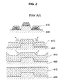
- FIG. 2 is a view illustrating a light emitting device disclosed in International Publication WO02/75821 and WO03/10831 , particularly, showing a process of growing a nitride semiconductor layer 410 on a patterned substrate 400.
- the nitride semiconductor layers 410 start to grow on lower and upper surfaces of the patterned substrate 400, respectively, and are brought into contact with each other. The growth of the nitride semiconductor layer 410 is facilitated in the contact portions to thereby form a flat surface. Since the patterned substrate 400 is used, light is scattered to improve external quantum efficiency, and crystal defects are reduced to improve quality of the nitride semiconductor layer 410.
- FIG. 3 is a view illustrating an example of a protrusion disclosed in WO03/10831 , particularly, a protrusion with a hexagonal cross-section on a substrate.
- a protrusion disclosed in WO03/10831
- the side of the protrusion is positioned in parallel with a stably growing face of a nitride semiconductor (e.g., a flat zone 401 of a substrate; refer to FIG. 4 )
- the nitride semiconductor grows slowly, which results in increase of crystal defects. So as to decrease the crystal defects, the entire sides of the protrusion are formed, crossing the stably growing face.
- Such a lateral constraint of the protrusion makes it difficult to form protrusions and/or depressions on the substrate to improve crystallinity.
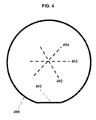
- FIG. 4 is an explanatory view illustrating stably growing faces of a nitride semiconductor, particularly, three stably growing faces 402, 403 and 404 with an angular difference of 60 ° on a C-surface sapphire substrate 400.
- the present invention has been made to solve the above-described shortcomings occurring in the prior art, and an object of the present invention is to provide a III-nitride semiconductor light emitting device which can solve the foregoing problems.
- Another object of the present invention is to provide a III-nitride semiconductor light emitting device which can not only solve a lateral constraint of a protrusion but also improve crystallinity.
- a further object of the present invention is to provide a III-nitride semiconductor light emitting device which can improve external quantum efficiency by adjusting an angle of a scribing line to a substrate having a protrusion.
- a still further object of the present invention is to provide a III-nitride semiconductor light emitting device which can secure a sufficient space for growing a nitride semiconductor on a substrate.
- a III-nitride semiconductor light emitting device including: a plurality of III-nitride semiconductor layers including an active layer for generating light by recombination of electrons and holes; and a substrate used to grow the plurality of III-nitride semiconductor layers, and including a protrusion with two opposite sides rounded.
- the protrusion includes two connection sides for connecting the two opposite rounded sides.
- the two connection sides are composed of straight lines, but may be slightly outwardly or inwardly curved in accordance with its mask pattern.
- the substrate is divided by at least one cutting surface, and extension lines of the two connection sides cross the at least one cutting surface.
- the at least cutting surface defines the contour of the light emitting device, and may be formed by means of a diamond cutting or scribing/breaking process.
- the substrate includes a first array with a plurality of protrusions formed thereon, and a second array with a plurality of protrusions formed thereon, and the plurality of protrusions of the first array and the plurality of protrusions of the second array are arranged in alternate positions.
- the III-nitride semiconductor light emitting device can not only solve a lateral constraint of a protrusion but also improve crystallinity.
- the III-nitride semiconductor light emitting device can improve external quantum efficiency by adjusting an angle of a scribing line to a substrate having a protrusion.
- the III-nitride semiconductor light emitting device can improve crystallinity of a nitride semiconductor layer by securing a sufficient space for growing a nitride semiconductor on a substrate.
- FIG. 5 is a view illustrating an example of a III-nitride semiconductor light emitting device according to the present invention.
- the III-nitride semiconductor light emitting device includes a sapphire substrate 10 with protrusions 90 formed thereon, a buffer layer 20 grown on the sapphire substrate 10, an n-type nitride semiconductor layer 30 grown on the buffer layer 20, an active layer 40 grown on the n-type nitride semiconductor layer 30, a p-type nitride semiconductor layer 50 grown on the active layer 40, a light transmitting electrode 60 formed on the p-type nitride semiconductor layer 50, a p-side electrode 70 formed on the light transmitting electrode 60, and an n-side electrode 80 formed on an n-type nitride semiconductor layer 31 exposed by mesa-etching the p-type nitride semiconductor layer 50 and the active layer 40.
- FIG. 6 is an explanatory view illustrating shape and arrangement of protrusions according to the present invention.
- the protrusions 90 are formed on the sapphire substrate 10.
- Each protrusion 90 has two rounded sides 91, and two connection sides 92 connecting the two rounded sides 91.
- the rounded sides 91 face a flat zone 401 of the sapphire substrate 10, i.e., a stably growing face of a nitride semiconductor.
- the sides 91 are rounded not to be parallel with the stably growing face, thereby preventing growth delay of a nitride semiconductor layer and subsequently reducing crystal defects.
- FIGS. 7 and 8 are explanatory views illustrating an example of a process of forming protrusions according to the present invention.
- a photoresist 11 is coated on a substrate 10, and a patterning process is carried out thereon.
- the patterning process is performed by means of a photo-etching process.
- a thickness of the photoresist 11 to be coated is changed according to a height of protrusions to be formed on the substrate 10. That is, the thickness of the photoresist is adjusted according to the target height of the protrusions.
- FIG. 8 shows a shape of the pattern.
- the pattern can be 4.2 ⁇ m in height H, 2.4 ⁇ m in width W, 1.6 ⁇ m in protrusion interval D1, and 0.8 ⁇ m in array interval D2, and cut in edge portions.
- FIG. 9 shows one example of protrusions formed by the above process. If necessary, the top surfaces of the protrusions can be flat. In this case, a nitride semiconductor is also grown on the top surfaces of the protrusions.
- the substrate 10 is etched normally by means of a reactive ion etching (RIE). Meanwhile, edges of the mask pattern are actively etched. Even if the mask pattern is not rounded, it is possible to form the protrusion 90 according to the present invention.
- a pattern with rounded edges or a baking process for rounding may be used.
- connection sides are formed in a straight line shape by the etching. In a case where the baking process is performed, the connection sides can be slightly curved.
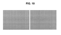
- FIG. 10 is an optical microscope photograph showing a GaN epitaxial layer grown on a prepared substrate according to the present invention.
- a focus was fixed on a boundary surface between the sapphire substrate and the epitaxial layer, and processed protrusions were projected on the sapphire substrate.
- a focus was fixed on a surface of the epitaxial layer, and a good epitaxial crystalline layer with a smooth surface was obtained without any pit or pinhole.
- a GaN layer with a thickness of about 4 ⁇ m was grown by means of MOCVD as follows.
- a prepared substrate was positioned on a susceptor made of graphite in an MOCVD reactor.
- a temperature was raised to 1100 °C in a hydrogen atmosphere to remove impurities from the surface of the substrate.
- SiC was grown by using 4.5 ⁇ mol of DTBSi per minute and 17 ⁇ mol of CBr 4 per minute as source material.
- the growth temperature was 950 °C and the growth time was 60 seconds, so that the layer was formed to an estimated thickness of 10 A.
- InGaN was grown by using 10 ⁇ mol of TMIn per minute, 400 ⁇ mol of TMGa per minute, and 12 I of NH 3 per minute as material source.
- the growth temperature was 500 °C and the growth time was 35 seconds, so that the layer was grown to a thickness of 500 A.
- an undoped GaN was formed by using 870 ⁇ mol of TMGa per minute and 18 I of NH 3 per minute as source material.
- the growth temperature was 1050 °C and the growth time was 7200 seconds, so that the layer was grown to a thickness of 4 ⁇ m.
- Crystallinity of the grown epitaxial layer could be confirmed by an XRD rocking curve measurement result.
- a half width of XRD (002) was ⁇ 250 arc-second, and a half width of XRD (102) was ⁇ 300 arc-second. That is, the epitaxial layer showed very high crystallinity.
- FIG. 11 is an explanatory view illustrating the relationship between a light emitting device and a scribing line.
- Quadrangular protrusions 90 are formed parallel to flat zone 401 of a substrate 10.
- Cutting surfaces 10a and 10b of each light emitting device, i.e., scribing lines are indicated by dotted lines.
- An amount of light to be extracted can be controlled by adjusting an angle y of the scribing line to the side of the quadrangular protrusion 90.
- FIG. 12 is a graph showing a simulation result of analyzing light extraction efficiency variations by an angle y, using a quadrangular pyramidal protrusion with a base of 4.5 ⁇ m ⁇ 3 ⁇ m.
- angle y is about 45 °, light extraction efficiency increases. This result can be identically applied to a protrusion with rounded sides.
- Light Tools 5.1 program of Optical research associates was used in the simulation.
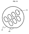
- FIG. 13 is a view illustrating another example of arrangement of protrusions according to the present invention.
- Protrusions 90 are formed on a sapphire substrate 10 in a position rotated against a flat zone 401.
- a scribing line is not adjusted according to a direction of the protrusions 90, but the direction of the protrusions 90 is adjusted according to the scribing line.
Landscapes
- Engineering & Computer Science (AREA)
- Manufacturing & Machinery (AREA)
- Computer Hardware Design (AREA)
- Microelectronics & Electronic Packaging (AREA)
- Power Engineering (AREA)
- Led Devices (AREA)
Applications Claiming Priority (2)
| Application Number | Priority Date | Filing Date | Title |
|---|---|---|---|
| KR1020070077218A KR20090012954A (ko) | 2007-07-31 | 2007-07-31 | 3족 질화물 반도체 발광소자 및 이를 제조하는 방법 |
| KR1020070106275A KR100896469B1 (ko) | 2007-10-22 | 2007-10-22 | 3족 질화물 반도체 발광소자 |
Publications (1)
| Publication Number | Publication Date |
|---|---|
| EP2020691A2 true EP2020691A2 (de) | 2009-02-04 |
Family
ID=39875202
Family Applications (1)
| Application Number | Title | Priority Date | Filing Date |
|---|---|---|---|
| EP08161500A Withdrawn EP2020691A2 (de) | 2007-07-31 | 2008-07-30 | Lichtemittierende III-Nitrid-Halbleiter-Vorrichtung |
Country Status (4)
| Country | Link |
|---|---|
| US (1) | US20090032835A1 (de) |
| EP (1) | EP2020691A2 (de) |
| JP (1) | JP2009038377A (de) |
| TW (1) | TW200913329A (de) |
Cited By (1)
| Publication number | Priority date | Publication date | Assignee | Title |
|---|---|---|---|---|
| EP2403019A3 (de) * | 2010-06-29 | 2014-06-18 | LG Innotek Co., Ltd. | Lichtemittierende Vorrichtung |
Families Citing this family (5)
| Publication number | Priority date | Publication date | Assignee | Title |
|---|---|---|---|---|
| CN106067501B (zh) | 2010-08-06 | 2019-03-12 | 日亚化学工业株式会社 | 蓝宝石基板及氮化物半导体发光元件 |
| KR20130137295A (ko) * | 2012-06-07 | 2013-12-17 | 엘지이노텍 주식회사 | 발광 소자 및 발광 소자 패키지 |
| CN103811592A (zh) * | 2012-11-12 | 2014-05-21 | 展晶科技(深圳)有限公司 | 发光二极管制造方法 |
| CN105449058A (zh) * | 2014-09-02 | 2016-03-30 | 展晶科技(深圳)有限公司 | 磊晶基板、磊晶基板的制造方法及发光二极管 |
| KR102284535B1 (ko) * | 2014-11-12 | 2021-08-02 | 서울바이오시스 주식회사 | 발광 소자 및 그 제조 방법 |
Citations (2)
| Publication number | Priority date | Publication date | Assignee | Title |
|---|---|---|---|---|
| WO2002075821A1 (fr) | 2001-03-21 | 2002-09-26 | Mitsubishi Cable Industries, Ltd. | Dispositif luminescent semiconducteur |
| WO2003010831A1 (en) | 2001-07-24 | 2003-02-06 | Nichia Corporation | Semiconductor light emitting device comprising uneven substrate |
Family Cites Families (6)
| Publication number | Priority date | Publication date | Assignee | Title |
|---|---|---|---|---|
| US6809802B1 (en) * | 1999-08-19 | 2004-10-26 | Canon Kabushiki Kaisha | Substrate attracting and holding system for use in exposure apparatus |
| JP3956941B2 (ja) * | 2001-06-15 | 2007-08-08 | 日亜化学工業株式会社 | 窒化物半導体発光素子及びそれを用いた発光装置 |
| JP4356723B2 (ja) * | 2001-07-24 | 2009-11-04 | 日亜化学工業株式会社 | 窒化物半導体発光素子の製造方法 |
| TW520616B (en) * | 2001-12-31 | 2003-02-11 | Ritdisplay Corp | Manufacturing method of organic surface light emitting device |
| KR100714639B1 (ko) * | 2003-10-21 | 2007-05-07 | 삼성전기주식회사 | 발광 소자 |
| KR100568297B1 (ko) * | 2004-03-30 | 2006-04-05 | 삼성전기주식회사 | 질화물 반도체 발광 소자 및 그 제조 방법 |
-
2008
- 2008-07-30 EP EP08161500A patent/EP2020691A2/de not_active Withdrawn
- 2008-07-30 JP JP2008197031A patent/JP2009038377A/ja active Pending
- 2008-07-31 US US12/183,351 patent/US20090032835A1/en not_active Abandoned
- 2008-07-31 TW TW097128951A patent/TW200913329A/zh unknown
Patent Citations (2)
| Publication number | Priority date | Publication date | Assignee | Title |
|---|---|---|---|---|
| WO2002075821A1 (fr) | 2001-03-21 | 2002-09-26 | Mitsubishi Cable Industries, Ltd. | Dispositif luminescent semiconducteur |
| WO2003010831A1 (en) | 2001-07-24 | 2003-02-06 | Nichia Corporation | Semiconductor light emitting device comprising uneven substrate |
Cited By (1)
| Publication number | Priority date | Publication date | Assignee | Title |
|---|---|---|---|---|
| EP2403019A3 (de) * | 2010-06-29 | 2014-06-18 | LG Innotek Co., Ltd. | Lichtemittierende Vorrichtung |
Also Published As
| Publication number | Publication date |
|---|---|
| TW200913329A (en) | 2009-03-16 |
| US20090032835A1 (en) | 2009-02-05 |
| JP2009038377A (ja) | 2009-02-19 |
Similar Documents
| Publication | Publication Date | Title |
|---|---|---|
| JP5370262B2 (ja) | 半導体発光チップおよび基板の加工方法 | |
| JP5179068B2 (ja) | 化合物半導体素子の製造方法 | |
| EP1596443B1 (de) | Lichtemittierende Vorrichtung | |
| CN100517583C (zh) | 化合物半导体器件晶片的制造方法及其制造的晶片和器件 | |
| US6613461B1 (en) | Gallium nitride-based compound semiconductor chip and method for producing the same, and gallium nitride-based compound semiconductor wafer | |
| US8822247B2 (en) | Optical semiconductor element and manufacturing method of the same | |
| JP2001085736A (ja) | 窒化物半導体チップの製造方法 | |
| KR101454821B1 (ko) | 결정성막, 디바이스, 및, 결정성막 또는 디바이스의 제조방법 | |
| JP2010103424A (ja) | 半導体発光素子の製造方法 | |
| JP2001176823A (ja) | 窒化物半導体チップの製造方法 | |
| EP1376664A1 (de) | Verfahren zur herstellung eines halbleiters mit gruppe-iii-nitridzusammensetzung und halbleiterbauelement mit gruppe-iii-nitridzusammensetzung | |
| WO2006041134A1 (ja) | 窒化化合物半導体素子およびその製造方法 | |
| EP2020691A2 (de) | Lichtemittierende III-Nitrid-Halbleiter-Vorrichtung | |
| US20090166650A1 (en) | Light-emitting device of group iii nitride-based semiconductor and manufacturing method thereof | |
| KR100956456B1 (ko) | 3족 질화물 반도체 발광소자 | |
| JP4710148B2 (ja) | 窒化物半導体チップの製造方法 | |
| JP5377016B2 (ja) | 半導体装置の製造方法 | |
| CN107305920B (zh) | 基板晶片以及ⅲ族氮化物半导体元件的制造方法 | |
| CN101359712B (zh) | Ⅲ族氮化物半导体发光器件 | |
| JP2006165070A (ja) | 窒化物半導体結晶の製造方法 | |
| JP5834952B2 (ja) | 窒化物半導体基板の製造方法 | |
| JP2009184860A (ja) | 基板およびエピタキシャルウェハ | |
| KR20140131891A (ko) | 3족 질화물 반도체 적층체 | |
| KR100896469B1 (ko) | 3족 질화물 반도체 발광소자 | |
| JP3471687B2 (ja) | 半導体基材及びその製造方法 |
Legal Events
| Date | Code | Title | Description |
|---|---|---|---|
| PUAI | Public reference made under article 153(3) epc to a published international application that has entered the european phase |
Free format text: ORIGINAL CODE: 0009012 |
|
| AK | Designated contracting states |
Kind code of ref document: A2 Designated state(s): AT BE BG CH CY CZ DE DK EE ES FI FR GB GR HR HU IE IS IT LI LT LU LV MC MT NL NO PL PT RO SE SI SK TR |
|
| AX | Request for extension of the european patent |
Extension state: AL BA MK RS |
|
| STAA | Information on the status of an ep patent application or granted ep patent |
Free format text: STATUS: THE APPLICATION IS DEEMED TO BE WITHDRAWN |
|
| 18D | Application deemed to be withdrawn |
Effective date: 20130201 |