EP2017635A1 - Magnetvorrichtung - Google Patents
Magnetvorrichtung Download PDFInfo
- Publication number
- EP2017635A1 EP2017635A1 EP07742940A EP07742940A EP2017635A1 EP 2017635 A1 EP2017635 A1 EP 2017635A1 EP 07742940 A EP07742940 A EP 07742940A EP 07742940 A EP07742940 A EP 07742940A EP 2017635 A1 EP2017635 A1 EP 2017635A1
- Authority
- EP
- European Patent Office
- Prior art keywords
- magnetic field
- magnetic
- substrate
- conductive layer
- generating device
- Prior art date
- Legal status (The legal status is an assumption and is not a legal conclusion. Google has not performed a legal analysis and makes no representation as to the accuracy of the status listed.)
- Withdrawn
Links
- 239000000758 substrate Substances 0.000 claims abstract description 55
- 230000006698 induction Effects 0.000 claims description 74
- 239000010410 layer Substances 0.000 description 44
- 239000010408 film Substances 0.000 description 7
- 229910017052 cobalt Inorganic materials 0.000 description 6
- 239000010941 cobalt Substances 0.000 description 6
- GUTLYIVDDKVIGB-UHFFFAOYSA-N cobalt atom Chemical compound [Co] GUTLYIVDDKVIGB-UHFFFAOYSA-N 0.000 description 6
- 239000000463 material Substances 0.000 description 5
- 230000009467 reduction Effects 0.000 description 5
- 238000000605 extraction Methods 0.000 description 4
- 230000035699 permeability Effects 0.000 description 4
- RYGMFSIKBFXOCR-UHFFFAOYSA-N Copper Chemical compound [Cu] RYGMFSIKBFXOCR-UHFFFAOYSA-N 0.000 description 3
- 239000000853 adhesive Substances 0.000 description 3
- 230000002238 attenuated effect Effects 0.000 description 3
- 229910052802 copper Inorganic materials 0.000 description 3
- 239000010949 copper Substances 0.000 description 3
- 238000000034 method Methods 0.000 description 3
- 239000004642 Polyimide Substances 0.000 description 2
- 230000001070 adhesive effect Effects 0.000 description 2
- 229910052782 aluminium Inorganic materials 0.000 description 2
- XAGFODPZIPBFFR-UHFFFAOYSA-N aluminium Chemical compound [Al] XAGFODPZIPBFFR-UHFFFAOYSA-N 0.000 description 2
- 229910000808 amorphous metal alloy Inorganic materials 0.000 description 2
- 230000000052 comparative effect Effects 0.000 description 2
- 230000000694 effects Effects 0.000 description 2
- 230000005611 electricity Effects 0.000 description 2
- PCHJSUWPFVWCPO-UHFFFAOYSA-N gold Chemical compound [Au] PCHJSUWPFVWCPO-UHFFFAOYSA-N 0.000 description 2
- 229910052737 gold Inorganic materials 0.000 description 2
- 239000010931 gold Substances 0.000 description 2
- 239000000696 magnetic material Substances 0.000 description 2
- 229920001721 polyimide Polymers 0.000 description 2
- 239000011347 resin Substances 0.000 description 2
- 229920005989 resin Polymers 0.000 description 2
- 239000010409 thin film Substances 0.000 description 2
- 229910000859 α-Fe Inorganic materials 0.000 description 2
- 239000012790 adhesive layer Substances 0.000 description 1
- 229910045601 alloy Inorganic materials 0.000 description 1
- 239000000956 alloy Substances 0.000 description 1
- 238000005452 bending Methods 0.000 description 1
- -1 for example Polymers 0.000 description 1
- 230000005389 magnetism Effects 0.000 description 1
- 229910052751 metal Inorganic materials 0.000 description 1
- 239000002184 metal Substances 0.000 description 1
- 229910001172 neodymium magnet Inorganic materials 0.000 description 1
- 238000007747 plating Methods 0.000 description 1
- 239000000843 powder Substances 0.000 description 1
- 229910000938 samarium–cobalt magnet Inorganic materials 0.000 description 1
- 239000004065 semiconductor Substances 0.000 description 1
- 238000005549 size reduction Methods 0.000 description 1
Images

Classifications
-
- G—PHYSICS
- G01—MEASURING; TESTING
- G01R—MEASURING ELECTRIC VARIABLES; MEASURING MAGNETIC VARIABLES
- G01R33/00—Arrangements or instruments for measuring magnetic variables
- G01R33/02—Measuring direction or magnitude of magnetic fields or magnetic flux
- G01R33/06—Measuring direction or magnitude of magnetic fields or magnetic flux using galvano-magnetic devices
- G01R33/09—Magnetoresistive devices
-
- G—PHYSICS
- G01—MEASURING; TESTING
- G01R—MEASURING ELECTRIC VARIABLES; MEASURING MAGNETIC VARIABLES
- G01R33/00—Arrangements or instruments for measuring magnetic variables
- G01R33/0011—Arrangements or instruments for measuring magnetic variables comprising means, e.g. flux concentrators, flux guides, for guiding or concentrating the magnetic flux, e.g. to the magnetic sensor
-
- G—PHYSICS
- G01—MEASURING; TESTING
- G01R—MEASURING ELECTRIC VARIABLES; MEASURING MAGNETIC VARIABLES
- G01R33/00—Arrangements or instruments for measuring magnetic variables
- G01R33/02—Measuring direction or magnitude of magnetic fields or magnetic flux
-
- G—PHYSICS
- G01—MEASURING; TESTING
- G01R—MEASURING ELECTRIC VARIABLES; MEASURING MAGNETIC VARIABLES
- G01R33/00—Arrangements or instruments for measuring magnetic variables
- G01R33/02—Measuring direction or magnitude of magnetic fields or magnetic flux
- G01R33/06—Measuring direction or magnitude of magnetic fields or magnetic flux using galvano-magnetic devices
- G01R33/063—Magneto-impedance sensors; Nanocristallin sensors
-
- G—PHYSICS
- G01—MEASURING; TESTING
- G01R—MEASURING ELECTRIC VARIABLES; MEASURING MAGNETIC VARIABLES
- G01R33/00—Arrangements or instruments for measuring magnetic variables
- G01R33/12—Measuring magnetic properties of articles or specimens of solids or fluids
- G01R33/18—Measuring magnetostrictive properties
-
- H—ELECTRICITY
- H10—SEMICONDUCTOR DEVICES; ELECTRIC SOLID-STATE DEVICES NOT OTHERWISE PROVIDED FOR
- H10N—ELECTRIC SOLID-STATE DEVICES NOT OTHERWISE PROVIDED FOR
- H10N50/00—Galvanomagnetic devices
- H10N50/01—Manufacture or treatment
Definitions
- the present invention relates to a magnetic device that is provided with a magnetic sensor.
- induction elements such as magnetic impedance elements are integrated on substrates such as semiconductors.
- induction elements such as magnetic impedance elements
- substrates such as semiconductors.
- a method that may be considered in order to apply a bias magnetic field to the magnetic impedance elements is, for example, to place magnets adjacent to the magnetic impedance elements (Patent document 1).
- applying a bias magnetic field by means of magnets in this manner poses various problems when applied to magnetic sensors as the magnetic field strength of the individual magnets is not uniform, and it is difficult to consistently apply a bias magnetic field having a constant value.
- a method of consistently applying a bias magnetic field having a uniform strength to magnetic impedance elements in which a spiral-shape or coil-shape conductive layer is formed adjacent to the magnetic impedance elements, and a bias magnetic field is generated by energizing this conductive layer (Patent document 2).
- Patent document 2 a magnetic sensor in which magnetic impedance elements are arranged along a coil center axis of a conductive layer formed in a coil shape, in particular, has the characteristic that it is possible to apply a strong bias magnetic field consistently to the magnetic impedance elements, this method is preferable as it enables highly accurate magnetic sensors to be obtained.
- the present invention was conceived in view of the above described circumstances, and it is an object thereof to provide a magnetic device that is provided with magnetic elements that can be manufactured with a small size and weight and at low cost.
- a first aspect of the present invention is a magnetic device that includes: a magnetic element; and a first magnetic field application device and a second magnetic field application device that are placed so as to sandwich the magnetic element, and that are used to apply a unidirectional bias magnetic field to the magnetic element.
- a second aspect of the present invention is the magnetic device according to the first aspect in which the first magnetic field application device and the second magnetic field application device each include an independent magnetic field generating device and an independent magnetic field induction device.
- a third aspect of the present invention is the magnetic device according to the first aspect in which the magnetic field induction devices of both the first magnetic field application device and the second magnetic field application device, and the magnetic element are placed on substantially the same plane.
- a fourth aspect of the present invention is a magnetic device that includes: a first substrate having a first conductive layer and a second conductive layer; a second substrate having a third conductive layer and a fourth conductive layer; a magnetic element that is placed between the first substrate and the second substrate; a first connecting portion that electrically connects the first conductive layer and the third conductive layer; a second connecting portion that electrically connects the second conductive layer and the fourth conductive layer; a coil-shaped first magnetic field generating device that includes the first conductive layer, the third conductive layer, and the first connecting portion; a coil-shaped second magnetic field generating device that includes the second conductive layer, the fourth conductive layer, and the second connecting portion; a first magnetic field induction device that passes through the center of the coil shape of the first magnetic field generating device; and a second magnetic field induction device that passes through the center of the coil shape of the second magnetic field generating device.
- a fifth aspect of the present invention is the magnetic device according to the fourth aspect in which there is further provided a third substrate that is placed between the first substrate and the second substrate, and the third substrate has a magnetic element housing portion that houses the magnetic element, a first housing portion that houses the first magnetic field induction device, and a second housing portion that houses the second magnetic field induction device, and the magnetic element housing portion is placed between the first housing portion and the second housing portion.
- the magnetic device of the present invention as a result of the first magnetic field application device and the second magnetic field application device being placed on both sides of the magnetic element, it is possible to apply a strong bias magnetic field to the magnetic element that is efficient unidirectionally, and it is possible to achieve a highly accurate magnetic sensor.
- a magnetic field generating device that is used to apply a bias magnetic field to a magnetic element can be located away from the magnetic element. Because of this, it is not necessary to form the magnetic field generating device in proximity to the magnetic element. As a result, it is possible to achieve reductions in the size, and particularly in the thickness of the overall magnetic device, and it is possible to improve the degree of freedom in the layout of the instrument on which the magnetic device is mounted.
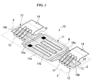
- FIG. 1 is a perspective view showing an example of the magnetic device (i.e., magnetic sensor) of the present invention.
- a magnetic device 10 of the present invention is provided with a magnetic element 11, and a first magnetic field application device 12 and second magnetic field application device 13 that are positioned so as to sandwich the magnetic element 11.
- the magnetic element 11 is obtained, for example, by forming a soft magnetic film 11 b in a meander pattern on a surface of a non-magnetic substrate 11 a.
- the first magnetic field application device 12 and second magnetic field application device 13 3 form a magnetic field M traveling in one direction S from the first magnetic field application device 12 towards the second magnetic field application device 13.
- the bias magnetic field M traveling in the one direction is applied to the entire soft magnetic film 11b.
- the magnetic device 10 having this structure, as a result of the first magnetic field application device 12 and the second magnetic field application device 13 being placed on both sides of the magnetic element 11, it is possible to apply a strong bias magnetic field to the magnetic element 11 that is efficient in the one direction, and it is possible to achieve a highly accurate magnetic sensor.
- a magnetic field generating device that is used to apply a bias magnetic field to the magnetic element 11 can be located away from the magnetic element 11, it is not necessary to form the magnetic field generating device in proximity to the magnetic element. As a result, it is possible to achieve reductions in the size, and particularly in the thickness of the overall magnetic device 10, and it is possible to improve the degree of freedom in the layout of the instrument on which the magnetic device 10 is mounted.
- the first magnetic field application device 12 and the second magnetic field application device 13 may also each be formed from an independent magnetic field generating device and an independent magnetic field induction device.
- the first magnetic field application device 12 has a first magnetic field generating device 15 and a first magnetic field induction device 16.
- the second magnetic field application device 13 has a second magnetic field generating device 17 and a second magnetic field induction device 18.
- Both ends of the first magnetic field generating device 15 and the second magnetic field generating device 17 are connected, for example, to a power supply 14, and may be formed by an inductor that is wound in a coil shape.
- the first magnetic field induction device 16 and the second magnetic field induction device 18 may be formed, for example, by arranging a high permeability material which is formed in a ribbon shape (i.e., in a thin belt shape) such that it passes through a center axis P of the respective coil shapes of the first magnetic field generating device 15 and the second magnetic field generating device 17.
- Ends 16a and 18a on one side of the first magnetic field induction device 16 and the second magnetic field induction device 18 which are formed in this ribbon shape (i.e., a thin belt shape) extend to positions adjacent to the magnetic element 11.
- Ends 16b and 18b on the other side of the first magnetic field induction device 16 and the second magnetic field induction device 18 are formed as open magnetic circuits in order to detect changes in the external magnetic field in the magnetic element 11.
- the first magnetic field application device 12 and the second magnetic field application device 13 each from an independent magnetic field generating device and an independent magnetic field induction device
- a solenoid coil for example, is used for the magnetic field application device
- the first magnetic field generating device 15 and the second magnetic field generating device 17 which are small-sized coils to be formed so as to envelop the first magnetic field induction device 16 and the second magnetic field induction device 18 which are formed from a thin, high permeability material in a ribbon shape without having to form in the vicinity of the magnetic element a coil which is a magnetic field generating device such that it envelops the comparatively large-sized magnetic element 11. Accordingly, it is possible to achieve a reduction in the thickness of the magnetic device 10.
- first magnetic field induction device 16 and the second magnetic field induction device 18 by extending the one ends 16a and 18a of the first magnetic field induction device 16 and the second magnetic field induction device 18 to positions adjacent to the magnetic element 11, even if the first magnetic field generating device 15 and the second magnetic field generating device 17 are formed at positions away from the magnetic element 11, it is possible for a bias magnetic field generated by these magnetic field generating devices 15 and 17 to be applied to the magnetic element 11 without being attenuated by the first magnetic field induction device 16 and the second magnetic field induction device 18.
- the high permeability material constituting the first magnetic field induction device 16 and the second magnetic field induction device 18 it is possible to use, for example, a cobalt-based amorphous thin ribbon or a sintered ferrite thin film or the like.
- a cobalt-based amorphous thin ribbon which has pliability is used for the first magnetic field induction device 16 and the second magnetic field induction device 18, then because it is possible to place the first magnetic field generating device 15 and the second magnetic field generating device 17 in positions away from the magnetic element 11, and induce a bias magnetic field in the magnetic element 11 by freely bending the first magnetic field induction device 16 and the second magnetic field induction device 18, it becomes possible to arrange the magnetic device 10 in an unrestricted layout in accordance with the shape of the instrument in which the magnetic device 10 is incorporated.
- the first magnetic field induction device 16 and second magnetic field induction device 18 and the magnetic element 11 may be placed on a substantially identical plane F.
- the bias magnetic field generated by the first magnetic field generating device 15 and the second magnetic field generating device 17 can be efficiently applied in the direction of the magnetic element 11 while any attenuation thereof is suppressed, thereby enabling a highly sensitive magnetic element 11 to be obtained.
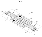
- FIG 2 is a perspective view showing another example of the magnetic device (i.e., magnetic sensor) of the present invention.
- a magnetic device 20 of this embodiment is provided with a first magnetic field application device 22 and a second magnetic field application device 23 which are placed so as to sandwich a magnetic element 21.
- the first magnetic field application device 22 is formed independently from a first magnetic field generating device 24 and a first magnetic field induction generating device 25, while the second magnetic field application device 23 is formed independently from a second magnetic field generating device 26 and a second magnetic field induction generating device 27.
- the first magnetic field generating device 24 and the second magnetic field generating device 26 are formed by permanent magnets, for example, made of NdFeB or SmCo or the like. A bias magnetic field generated by these permanent magnets is inducted to the magnetic element 21 by means of the first magnetic field induction generating device 25 and the second magnetic field induction generating device 27, so that a unidirectional bias magnetic field is applied to the magnetic element 21.
- permanent magnets for the first magnetic field generating device 24 and the second magnetic field generating device 26 it is possible to generate a bias magnetic field without having to supply electricity. Because of this, compared with a magnetic device which uses a solenoid coil or the like, it is possible to simplify the structure, and achieve reductions in both size and weight.
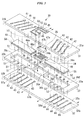
- FIG 3 is an exploded perspective view showing another example of the magnetic device of the present invention.
- a magnetic device 30 has a first substrate 31, a second substrate 32, a magnetic element 34 which is sandwiched between the first substrate 31 and the second substrate 32, and a first magnetic field induction device 48 and a second magnetic field induction device 49 which are placed so as to sandwich the magnetic element 34 from both sides thereof.
- a driver chip 35 to be placed between the first substrate 31 and the second substrate 32, and for a third substrate 33 to be provided to house the magnetic element 34 and the driver chip 35.
- First conductive layers 41, second conductive layers 42, and extraction conductive layers 45 are formed on a surface 31a of the first substrate 31.
- Third conductive layers 43 and fourth conductive layers 44 are formed on a surface 32a of the second substrate 32.
- the magnetic element 34 is obtained, for example, by forming a soft magnetic film 34b in a meander pattern on a surface of a non-magnetic substrate 34a, and electrode pads 46a and 46b are formed on both ends of the soft magnetic film 34b. When a bias magnetic field is applied to this magnetic element 34, output signals therefrom are changed in accordance with the size of the magnetic field.
- the driver chip 35 is an integrated circuit that controls the magnetic element 34, and electrode pads 47a and 47b are formed on a surface thereof.
- a first non-conductive layer 54, and a second non-conductive layer 55 that insulate the first magnetic field induction device 48 and the second magnetic field induction device 49 from the third conductive layers 43 and the fourth conductive layers 44 are formed respectively on the second substrate 32 side of the first magnetic field induction device 48 and the second magnetic field induction device 49.
- Third linking portions 53 which are formed from conductive paste or copper plating or the like that penetrate from the one surface 31 a to the other surface 31 b of the first substrate 31 and electrically connect the extraction conductive layers 45 respectively to the electrode pads 46a and 46b of the magnetic element 34 and electrode pads 47a and 47b of the driver chip 35 are formed in the first substrate 31.
- a magnetic element housing portion 36a that houses the magnetic element 34
- a chip housing portion 36b that houses the driver chip 35
- a first housing portion 36c that houses the first magnetic field induction device 48
- a second housing portion 36d that houses the second magnetic field induction device 49.
- first connecting portions 51 which are formed from conductive paste that penetrate from one surface 33a to another surface 33b of the third substrate 33 and electrically connect the first conductive layers 41 to the second conductive layers 43 are formed in the third substrate 33
- second connecting portions 52 which are formed from conductive paste that penetrate from one surface 33a to another surface 33b of the third substrate 33 and electrically connect the second conductive layers 42 to the fourth conductive layers 44 are formed in the third substrate 33.
- a coil-shaped first magnetic field generating device 57 that envelops the periphery of the first magnetic field induction device 48, and a coil-shaped second magnetic field generating device 58 that envelops the periphery of the second magnetic field induction device 49 are formed respectively.
- a first magnetic field application device 61 is formed by the first magnetic field generating device 57 and the first magnetic field induction device 48, and a second magnetic field application device 62 is formed by the second magnetic field generating device 58 and the second magnetic field induction device 49.
- the electrode pads 57a and 57b at both ends of the first magnetic field generating device 57 and the electrode pads 58a and 58b at both ends of the second magnetic field generating device 58 magnetic fields are generated in the first magnetic field generating device 57 and the second magnetic field generating device 58.
- the magnetic fields which are generated in the first magnetic field generating device 57 and the second magnetic field generating device 58 are inducted to the magnetic element 34 respectively by the first magnetic field induction device 48 and the second magnetic field induction device 49.
- a unidirectional, strong bias magnetic field M is applied to the magnetic element 34.
- the first magnetic field generating device 57 and the second magnetic field generating device 58 are formed respectively in a compact coil shape so as to sandwich the magnetic element 34 from both sides while being isolated therefrom, and the bias magnetic fields which are generated by this first magnetic field generating device 57 and second magnetic field generating device 58 can be inducted by the first magnetic field induction device 48 and the second magnetic field induction device 49 without being attenuated thereby, and applied to the magnetic element 34. Accordingly, it is possible to achieve a small, lightweight magnetic device that can be manufactured at low cost.
- the first substrate 31 may be formed from a nonconductive resin such as, for example polyimide.
- the first conductive layers 41, the second conductive layers 42, and the extraction conductive layer 45 which are formed on the first substrate 31 may also be formed on the other surface 31 b on the opposite side from the one surface 31 a of the first substrate 31.
- the first conductive layers 41, the second conductive layers 42, and the extraction conductive layer 45 may be formed from a material having superior conductivity such as, for example, copper, aluminum, gold, or the like.
- the soft magnetic film 34b that makes up the magnetic element 34 is, for example, an amorphous soft magnetic material.
- the shape of the soft magnetic film 34b is one that makes it possible to detect magnetism with a high degree of accuracy, then any type of shape may be used in addition to a meandering shape.
- the first connecting portions 51, the second connecting portions 52, and the third connecting portions 53 may be a conductive paste which is formed by dispersing a fine powder of conductive metal in an adhesive medium.
- the first magnetic field induction device 48 and the second magnetic field induction device 49 it is possible to use, for example, a cobalt-based amorphous thin ribbon or a sintered ferrite thin film or the like.
- the first substrate 31 and the second substrate 32 are joined so as to sandwich the third substrate 33 using the first connecting portions 51 and the second connecting portions 52 which are formed from the aforementioned adhesive conductive paste, however, in addition to this it is also possible to employ a structure in which the respective layers are joined together by forming adhesive layers using an adhesive agent or the like between the first substrate 31 and the third substrate 33, and between the third substrate 33 and the second substrate 32.
- the second substrate 32 may be formed from a nonconductive resin such as, for example, polyimide.
- the third conductive layer 43 and the fourth conductive layer 44 which are formed on the second substrate 32 may also be formed on the other surface 32b on the opposite side from the one surface 32a of the second substrate 32.
- the third conductive layer 43 and the fourth conductive layer 44 may be formed from a material having superior conductivity such as, for example, copper, aluminum, gold, or the like.
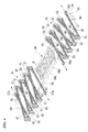
- FIG. 5 is an exploded perspective view showing another example of the magnetic device of the present invention.
- a magnetic device 70 has a first substrate 71, a second substrate 72, a magnetic element 73 which is sandwiched between the first substrate 71 and the second substrate 72, and a first magnetic field application device 74 and a second magnetic field application device 75 which are placed so as to sandwich the magnetic element 73 from both sides thereof.
- the first magnetic field application device 74 is formed by the first magnetic field generating device 76 and the first magnetic field induction device 77.
- the second magnetic field application device 75 is formed by the second magnetic field generating device 78 and the second magnetic field induction device 79.
- permanent magnets are used for the first magnetic field generating device 76 and the second magnetic field generating device 78.
- the bias magnetic fields which are generated by the first magnetic field generating device 76 and second magnetic field generating device 78 which are permanent magnets, can be applied to the magnetic element 73 by the first magnetic field induction device 77 and the second magnetic field induction device 79 without being attenuated thereby.
- magnets as magnetic field generating devices in this manner, it is possible to generate a bias magnetic field without having to supply electricity. Because of this, compared with a magnetic device which uses a solenoid coil or the like, it is possible to simplify the structure, and achieve reductions in both size and weight of the magnetic device 70.
- the effects of the magnetic induction device constructed from a high permeability magnetic material of the present invention were tested.
- a film of CoZrNb was formed in a meander pattern on a Si substrate having a chip size of 2.5 mm ⁇ 1.2 mm ⁇ 625 ⁇ m so as to provide a magnetic element.
- the bias magnetic field of this magnetic element was 8 (Oe).
- a ribbon-shaped cobalt-based amorphous alloy having a width of approximately 1 mm and a thickness of 20 ⁇ m was used for the magnetic field induction devices.
- 0.2A of current was supplied to coil-shaped magnetic field application devices having 120 turns in the coil.
- the spacing between end portions of the magnetic field induction devices and the magnetic element was 1 mm.
Landscapes
- Physics & Mathematics (AREA)
- Condensed Matter Physics & Semiconductors (AREA)
- General Physics & Mathematics (AREA)
- Chemical & Material Sciences (AREA)
- Engineering & Computer Science (AREA)
- Nanotechnology (AREA)
- Measuring Magnetic Variables (AREA)
- Hall/Mr Elements (AREA)
- Hard Magnetic Materials (AREA)
Applications Claiming Priority (2)
| Application Number | Priority Date | Filing Date | Title |
|---|---|---|---|
| JP2006130015A JP2007303860A (ja) | 2006-05-09 | 2006-05-09 | 磁気デバイス |
| PCT/JP2007/059505 WO2007129705A1 (ja) | 2006-05-09 | 2007-05-08 | 磁気デバイス |
Publications (2)
| Publication Number | Publication Date |
|---|---|
| EP2017635A1 true EP2017635A1 (de) | 2009-01-21 |
| EP2017635A4 EP2017635A4 (de) | 2012-03-14 |
Family
ID=38667813
Family Applications (1)
| Application Number | Title | Priority Date | Filing Date |
|---|---|---|---|
| EP07742940A Withdrawn EP2017635A4 (de) | 2006-05-09 | 2007-05-08 | Magnetvorrichtung |
Country Status (5)
| Country | Link |
|---|---|
| US (2) | US7782049B2 (de) |
| EP (1) | EP2017635A4 (de) |
| JP (1) | JP2007303860A (de) |
| CN (1) | CN101438178B (de) |
| WO (1) | WO2007129705A1 (de) |
Families Citing this family (12)
| Publication number | Priority date | Publication date | Assignee | Title |
|---|---|---|---|---|
| WO2008120118A2 (en) * | 2007-03-30 | 2008-10-09 | Nxp B.V. | Magneto-resistive sensor |
| US8269490B2 (en) * | 2009-04-03 | 2012-09-18 | Honeywell International Inc. | Magnetic surface acoustic wave sensor apparatus and method |
| HU229031B1 (en) | 2009-12-21 | 2013-07-29 | Egis Gyogyszergyar Nyilvanosan Muekoedoe Reszvenytarsasag | Process for producing prasurgel and its intermediate |
| JP5761787B2 (ja) * | 2011-03-15 | 2015-08-12 | 国立大学法人信州大学 | センサおよびその調整方法 |
| JP6370768B2 (ja) * | 2015-11-26 | 2018-08-08 | 矢崎総業株式会社 | 磁界検出センサ |
| US20170234942A1 (en) * | 2016-02-11 | 2017-08-17 | Texas Instruments Incorporated | Layouts for interlevel crack prevention in fluxgate technology manufacturing |
| CN106646278B (zh) * | 2016-12-09 | 2019-05-24 | 中国人民解放军国防科学技术大学 | 一种利用高分辨力磁场探测的低噪声mems前置放大器件 |
| US10257933B1 (en) * | 2017-09-26 | 2019-04-09 | Google Llc | Transverse circuit board to route electrical traces |
| JP7259293B2 (ja) * | 2018-11-29 | 2023-04-18 | 株式会社レゾナック | 磁気センサおよび磁気センサの製造方法 |
| US11131727B2 (en) * | 2019-03-11 | 2021-09-28 | Tdk Corporation | Magnetic sensor device |
| JP7395978B2 (ja) * | 2019-11-14 | 2023-12-12 | 株式会社レゾナック | 磁気センサ |
| KR20240032897A (ko) * | 2021-07-16 | 2024-03-12 | 액트 아이덴티티 테크놀로지 리미티드 | 칩 모듈 및 이를 형성하는 방법 |
Family Cites Families (8)
| Publication number | Priority date | Publication date | Assignee | Title |
|---|---|---|---|---|
| US6150809A (en) * | 1996-09-20 | 2000-11-21 | Tpl, Inc. | Giant magnetorestive sensors and sensor arrays for detection and imaging of anomalies in conductive materials |
| JP2001221838A (ja) | 2000-02-09 | 2001-08-17 | Alps Electric Co Ltd | 磁気インピーダンス効果素子及びその製造方法 |
| JP3831584B2 (ja) | 2000-07-21 | 2006-10-11 | アルプス電気株式会社 | 磁気インピーダンス効果素子 |
| JP2003167037A (ja) * | 2001-11-30 | 2003-06-13 | Tama Electric Co Ltd | 磁気センサ |
| US6566872B1 (en) * | 2001-12-31 | 2003-05-20 | Xenosensors, Inc. | Magnetic sensor device |
| JP4014875B2 (ja) * | 2002-01-15 | 2007-11-28 | 伸▲よし▼ 杉谷 | 磁気検知装置 |
| KR100619369B1 (ko) * | 2004-07-24 | 2006-09-08 | 삼성전기주식회사 | 미약자계 감지용 센서를 구비한 인쇄회로기판 및 그 제작방법 |
| CN101065721B (zh) * | 2004-09-27 | 2010-08-11 | Nxp股份有限公司 | 用于输入设备的磁传感器 |
-
2006
- 2006-05-09 JP JP2006130015A patent/JP2007303860A/ja active Pending
-
2007
- 2007-05-08 WO PCT/JP2007/059505 patent/WO2007129705A1/ja not_active Ceased
- 2007-05-08 CN CN2007800164349A patent/CN101438178B/zh not_active Expired - Fee Related
- 2007-05-08 EP EP07742940A patent/EP2017635A4/de not_active Withdrawn
-
2008
- 2008-11-07 US US12/267,169 patent/US7782049B2/en not_active Expired - Fee Related
-
2010
- 2010-01-13 US US12/686,840 patent/US7772841B2/en not_active Expired - Fee Related
Also Published As
| Publication number | Publication date |
|---|---|
| EP2017635A4 (de) | 2012-03-14 |
| CN101438178B (zh) | 2011-11-16 |
| US7782049B2 (en) | 2010-08-24 |
| US20090066326A1 (en) | 2009-03-12 |
| WO2007129705A1 (ja) | 2007-11-15 |
| US7772841B2 (en) | 2010-08-10 |
| CN101438178A (zh) | 2009-05-20 |
| JP2007303860A (ja) | 2007-11-22 |
| US20100109663A1 (en) | 2010-05-06 |
Similar Documents
| Publication | Publication Date | Title |
|---|---|---|
| EP2017635A1 (de) | Magnetvorrichtung | |
| US10054466B2 (en) | Electromagnetic induction sensor, overlay member for electromagnetic induction sensor, and manufacturing method of electromagnetic induction sensor | |
| JP4458149B2 (ja) | 磁気カプラ | |
| CN100356605C (zh) | 磁性传感器及其制造方法 | |
| EP2174152B1 (de) | Stromsensor mit zwischenangeordneter schicht für magnetische permeabilität | |
| JP3621655B2 (ja) | Rfidタグ構造及びその製造方法 | |
| DK2546843T3 (en) | Magnetic element for wireless power transfer and power supply arrangement | |
| US7859258B2 (en) | Magnetic sensor and magnetic sensor module | |
| US6650112B2 (en) | Magnetics impedance element having a thin film magnetics core | |
| EP0856855A2 (de) | Gedruckte Spule mit magnetischer Schicht | |
| US6998840B2 (en) | Fluxgate sensor integrated having stacked magnetic cores in printed circuit board and method for manufacturing the same | |
| US7495624B2 (en) | Apparatus for detection of the gradient of a magnetic field, and a method for production of the apparatus | |
| US20230290563A1 (en) | Radio frequency weak magnetic field detection sensor and method of manufacturing the same | |
| US11366181B2 (en) | Component carrier with integrated flux gate sensor | |
| JP2001004726A (ja) | 磁界センサ | |
| EP0930508A1 (de) | Magnetoimpedanzeffektvorrichtung | |
| US20240329163A1 (en) | Monitoring unit comprising an integrated magnetic field sensor | |
| JP2007512696A (ja) | 高周波薄膜電子回路素子 | |
| JP2001159668A (ja) | 薄膜電子部品 | |
| KR101813408B1 (ko) | 자성체를 포함하는 무선 통신 안테나 | |
| CN118275530A (zh) | 一种基于低温共烧陶瓷工艺的涡流传感器 |
Legal Events
| Date | Code | Title | Description |
|---|---|---|---|
| PUAI | Public reference made under article 153(3) epc to a published international application that has entered the european phase |
Free format text: ORIGINAL CODE: 0009012 |
|
| 17P | Request for examination filed |
Effective date: 20081016 |
|
| AK | Designated contracting states |
Kind code of ref document: A1 Designated state(s): AT BE BG CH CY CZ DE DK EE ES FI FR GB GR HU IE IS IT LI LT LU LV MC MT NL PL PT RO SE SI SK TR |
|
| AX | Request for extension of the european patent |
Extension state: AL BA HR MK RS |
|
| RBV | Designated contracting states (corrected) |
Designated state(s): DE GB |
|
| A4 | Supplementary search report drawn up and despatched |
Effective date: 20120214 |
|
| RIC1 | Information provided on ipc code assigned before grant |
Ipc: G01R 33/00 20060101ALI20120208BHEP Ipc: H01L 43/00 20060101ALI20120208BHEP Ipc: G01R 33/02 20060101AFI20120208BHEP |
|
| STAA | Information on the status of an ep patent application or granted ep patent |
Free format text: STATUS: THE APPLICATION HAS BEEN WITHDRAWN |
|
| 18W | Application withdrawn |
Effective date: 20120618 |
|
| DAX | Request for extension of the european patent (deleted) |