EP2174152B1 - Stromsensor mit zwischenangeordneter schicht für magnetische permeabilität - Google Patents
Stromsensor mit zwischenangeordneter schicht für magnetische permeabilität Download PDFInfo
- Publication number
- EP2174152B1 EP2174152B1 EP08826498.1A EP08826498A EP2174152B1 EP 2174152 B1 EP2174152 B1 EP 2174152B1 EP 08826498 A EP08826498 A EP 08826498A EP 2174152 B1 EP2174152 B1 EP 2174152B1
- Authority
- EP
- European Patent Office
- Prior art keywords
- current
- sensor
- magnetic field
- magnetic
- current sensor
- Prior art date
- Legal status (The legal status is an assumption and is not a legal conclusion. Google has not performed a legal analysis and makes no representation as to the accuracy of the status listed.)
- Not-in-force
Links
- 230000005291 magnetic effect Effects 0.000 title claims description 132
- 230000035699 permeability Effects 0.000 title description 9
- 239000000463 material Substances 0.000 claims description 38
- RYGMFSIKBFXOCR-UHFFFAOYSA-N Copper Chemical compound [Cu] RYGMFSIKBFXOCR-UHFFFAOYSA-N 0.000 claims description 13
- 229910052802 copper Inorganic materials 0.000 claims description 13
- 239000010949 copper Substances 0.000 claims description 13
- 230000005355 Hall effect Effects 0.000 claims description 12
- 239000004065 semiconductor Substances 0.000 claims description 10
- 239000000758 substrate Substances 0.000 claims description 10
- 230000004907 flux Effects 0.000 claims description 5
- 229910052751 metal Inorganic materials 0.000 claims description 2
- 239000002184 metal Substances 0.000 claims description 2
- 239000004020 conductor Substances 0.000 description 81
- 239000010410 layer Substances 0.000 description 35
- XEEYBQQBJWHFJM-UHFFFAOYSA-N Iron Chemical group [Fe] XEEYBQQBJWHFJM-UHFFFAOYSA-N 0.000 description 14
- 238000005259 measurement Methods 0.000 description 10
- 230000008901 benefit Effects 0.000 description 5
- 238000013461 design Methods 0.000 description 5
- 238000012216 screening Methods 0.000 description 5
- SXHLTVKPNQVZGL-UHFFFAOYSA-N 1,2-dichloro-3-(3-chlorophenyl)benzene Chemical compound ClC1=CC=CC(C=2C(=C(Cl)C=CC=2)Cl)=C1 SXHLTVKPNQVZGL-UHFFFAOYSA-N 0.000 description 4
- XUIMIQQOPSSXEZ-UHFFFAOYSA-N Silicon Chemical compound [Si] XUIMIQQOPSSXEZ-UHFFFAOYSA-N 0.000 description 4
- 238000010586 diagram Methods 0.000 description 4
- 230000005672 electromagnetic field Effects 0.000 description 4
- 238000012545 processing Methods 0.000 description 4
- 229910052710 silicon Inorganic materials 0.000 description 4
- 239000010703 silicon Substances 0.000 description 4
- 230000000694 effects Effects 0.000 description 3
- 230000005684 electric field Effects 0.000 description 3
- 239000000696 magnetic material Substances 0.000 description 3
- 238000000034 method Methods 0.000 description 3
- 229910000595 mu-metal Inorganic materials 0.000 description 3
- PXHVJJICTQNCMI-UHFFFAOYSA-N Nickel Chemical compound [Ni] PXHVJJICTQNCMI-UHFFFAOYSA-N 0.000 description 2
- 239000000853 adhesive Substances 0.000 description 2
- 230000001070 adhesive effect Effects 0.000 description 2
- 229910045601 alloy Inorganic materials 0.000 description 2
- 239000000956 alloy Substances 0.000 description 2
- 239000003302 ferromagnetic material Substances 0.000 description 2
- 230000036039 immunity Effects 0.000 description 2
- 229910052742 iron Inorganic materials 0.000 description 2
- UGKDIUIOSMUOAW-UHFFFAOYSA-N iron nickel Chemical class [Fe].[Ni] UGKDIUIOSMUOAW-UHFFFAOYSA-N 0.000 description 2
- 238000004519 manufacturing process Methods 0.000 description 2
- 238000001465 metallisation Methods 0.000 description 2
- 238000012544 monitoring process Methods 0.000 description 2
- 229910000889 permalloy Inorganic materials 0.000 description 2
- 230000008569 process Effects 0.000 description 2
- 229910000881 Cu alloy Inorganic materials 0.000 description 1
- 229910000640 Fe alloy Inorganic materials 0.000 description 1
- CWYNVVGOOAEACU-UHFFFAOYSA-N Fe2+ Chemical compound [Fe+2] CWYNVVGOOAEACU-UHFFFAOYSA-N 0.000 description 1
- 229910001030 Iron–nickel alloy Inorganic materials 0.000 description 1
- ZOKXTWBITQBERF-UHFFFAOYSA-N Molybdenum Chemical compound [Mo] ZOKXTWBITQBERF-UHFFFAOYSA-N 0.000 description 1
- 230000003321 amplification Effects 0.000 description 1
- 230000008859 change Effects 0.000 description 1
- 238000004891 communication Methods 0.000 description 1
- 239000000470 constituent Substances 0.000 description 1
- -1 copper Chemical class 0.000 description 1
- GOECOOJIPSGIIV-UHFFFAOYSA-N copper iron nickel Chemical compound [Fe].[Ni].[Cu] GOECOOJIPSGIIV-UHFFFAOYSA-N 0.000 description 1
- 208000002925 dental caries Diseases 0.000 description 1
- 238000001514 detection method Methods 0.000 description 1
- 238000003745 diagnosis Methods 0.000 description 1
- 230000005670 electromagnetic radiation Effects 0.000 description 1
- 238000005516 engineering process Methods 0.000 description 1
- 230000005294 ferromagnetic effect Effects 0.000 description 1
- 238000001914 filtration Methods 0.000 description 1
- 238000009533 lab test Methods 0.000 description 1
- 150000002739 metals Chemical class 0.000 description 1
- 238000012986 modification Methods 0.000 description 1
- 230000004048 modification Effects 0.000 description 1
- 229910052750 molybdenum Inorganic materials 0.000 description 1
- 239000011733 molybdenum Substances 0.000 description 1
- 238000010137 moulding (plastic) Methods 0.000 description 1
- 229910052759 nickel Inorganic materials 0.000 description 1
- 238000003199 nucleic acid amplification method Methods 0.000 description 1
- 230000004044 response Effects 0.000 description 1
- 238000012552 review Methods 0.000 description 1
- 230000035945 sensitivity Effects 0.000 description 1
- 239000002356 single layer Substances 0.000 description 1
- 230000003068 static effect Effects 0.000 description 1
- 238000003466 welding Methods 0.000 description 1
Images



Classifications
-
- G—PHYSICS
- G01—MEASURING; TESTING
- G01R—MEASURING ELECTRIC VARIABLES; MEASURING MAGNETIC VARIABLES
- G01R33/00—Arrangements or instruments for measuring magnetic variables
- G01R33/02—Measuring direction or magnitude of magnetic fields or magnetic flux
- G01R33/06—Measuring direction or magnitude of magnetic fields or magnetic flux using galvano-magnetic devices
- G01R33/07—Hall effect devices
-
- G—PHYSICS
- G01—MEASURING; TESTING
- G01R—MEASURING ELECTRIC VARIABLES; MEASURING MAGNETIC VARIABLES
- G01R15/00—Details of measuring arrangements of the types provided for in groups G01R17/00 - G01R29/00, G01R33/00 - G01R33/26 or G01R35/00
- G01R15/14—Adaptations providing voltage or current isolation, e.g. for high-voltage or high-current networks
- G01R15/20—Adaptations providing voltage or current isolation, e.g. for high-voltage or high-current networks using galvano-magnetic devices, e.g. Hall-effect devices, i.e. measuring a magnetic field via the interaction between a current and a magnetic field, e.g. magneto resistive or Hall effect devices
- G01R15/207—Constructional details independent of the type of device used
Definitions
- the present invention relates generally to electric current sensors based on magnetic field sensing.
- State-of-the-art magnetic field-based current sensors generally include a magnetic field sensor, an iron core, and an amplifier.
- the iron core surrounds an electrical conductor, preferably comprising copper for carrying the current to be measured, the current causing a magnetic field corresponding to the intensity of the current to be generated in the iron core.
- the magnetic field sensor is arranged in a gap in the iron core. Thus, the field lines of the magnetic field induced in the iron core by the current to be measured pass through the magnetic field sensor.
- the magnetic field sensor generates an electrical output signal generally proportional to be current to be measured, and this signal is amplified by an amplifier, such as an operational amplifier.
- the iron core in conventional current sensors primarily provides two functions. First, the conducting of the magnetic field induced by the current to be measured through the magnetic field sensor, and second, the screening of the magnetic field sensor from extraneous electric and magnetic fields which are known to cause measurement error.
- the use of iron cores results in a sensor cost that is too expensive for many applications.
- the primary conductor which carries the current to be measured comprises an electrically conducting ferritic material generally mixed with an electrically conducting material (e.g. copper).
- the primary conductor at least partially surrounds the magnetic field sensor which assumes the functions of the iron core.
- the magnetic field sensor is centered near a notch in the primary conductor which serves to focus the magnetic flux lines from the primary current in the primary conductor that reaches the magnetic field sensor.
- the current sensor design disclosed in EP 1192473 / WO 00/79291 generally has the disadvantage that the electromagnetic field associated with the current to be measured generates a magnetic field in the primary conductor, which can prevent precise measurement of the magnetic field associated with the current to be measured in the notch by adding another magnetic field component.
- the remanance of the primary conductor also causes non-linearity and magnetic saturation in the region of the notch which degrades the effect of the focussing notch. If only magnetic permeable material is used for the primary conductor (without copper or other electrical conductor), then a large cross-sectional area of this expensive material is generally needed because of its relatively high electrical resistivity.
- sensors disclosed in EP 1192473 / WO 00/79291 having a primary conductor including magnetic permeable material mixed with electrically conducting material can provide good performance and a reduced cost compared to conventional iron core-based current sensors, in certain important applications more precise measurement of electric current is required. Precise measurement of electric current requires improved linearity (between the current to be measured flowing as primary current and the magnetic flux reaching the magnetic sensor) and reduced resistive impedance. Lower cost would also be helpful.
- Some present current sensor applications include measurement of electric current include motor current control in frequency inverters, phase current control in servo-drives, overload protection for motors and power semiconductors, control of energy systems (e. g. wind energy), current control and monitoring in welding equipment, current regulation in switching mode power supplies, current control in uninterruptible power supplies, battery current diagnosis in motor vehicles, ground fault detection and laboratory test equipment. Some of these applications generally require precise current measurements.
- US5642041A discloses an alternating current sensor, including a first conductor plate, a second conductor plate positioned in spaced relationship relative to the first conductor plate and facing the first conductor plate, and a third conductor plate for electrically interconnecting the first and second conductor plates to form a connected conductive path along the first and second conductor plates.
- the first and second conductor plates are shaped to form respective magnetic field constituents around each of the first and second conductor plates during current flow along the conductive path.
- a sensor made up of one or more air-core coils, is provided for sensing changes in magnetic flux within a predetermined region, such as in a passage between the first and second conductor plates and/or near respective outer surfaces of the first and second conductor plates.
- US4890083A discloses a shield for electromagnetic radiations, comprising a laminated sheet having exterior layers of copper which sandwich an interior layer of a ferromagnetic alloy taken from the class consisting of nickel-iron compounds. The layers are metallurgically bonded to each other. According to a second embodiment, a laminated sheet is provided having exterior layers of copper which sandwich plural interior layers of ferromagnetic material.
- US2005030004A1 discloses a current sensor provided with a U-shaped conductor, through which current under measurement flows, a magnetic sensor disposed between two straight portions parallel to each other both of which form the U-shaped conductor, a magnetic material of surrounding shape which surrounds the two straight portions and the magnetic sensor and includes a convex opposed to the magnetic sensor and a supporting member for supporting the conductor, the magnetic sensor and the magnetic material so as to position ends of the conductor and terminals of the magnetic sensor at the same side with respect to the magnetic material.
- WO0079291A1 discloses a current sensor for measuring a current which is conveyed by a current conductor, comprising a magnetic field sensor and an amplifier which is associated with said magnetic field sensor.
- the current conductor is made of a conductive, ferritic material and is strip-like in form.
- the current conductor encompasses the magnetic field sensor in an at least partial manner.
- JP60214404 discloses a magnetic head shield to improve the S/N of a reproduced output by providing a shield member having a high electric conductivity such as copper so as to strengthen the shield effect especially against a high frequency electromagnetic field.
- the high electric conductivity material and the high permeability material (such as Permalloy) are formed as a sandwich in this case and it is also considered that they are used individually or combined together.
- the high permeability material and the high electric conductivity material are separated by a cushion member or the like.
- US4559495A discloses a transducer free of any magnetic core for contactless measurement of a current, including an electrically conducting strip adapted to carry the current in a predetermined direction.
- a first magnetic field sensor near one side measures the first primary magnetic field at right angles to the predetermined direction and provides a first output signal
- a second magnetic field sensor near the other side of the strip measures the second primary magnetic field which has a direction opposite to the predetermined direction, and provides a second output signal.
- a circuit processes the first and second output signals, and generates an output signal proportional to the measured current.
- the present invention provides a current sensor according to claim 1 of the appended claims.
- the invention further provides a control system according to claim 7 of the appended claims.
- a current sensor comprises a magnetic field sensor, a primary conductor comprising sandwich comprising an electrically conducting top layer and electrically conducting bottom layer, and a layer of magnetic permeable material interposed between.
- the magnetic permeable material is disposed around the magnetic field sensor so that the magnetic field sensor is at least partially surrounded by the magnetic permeable material which thus provides field screening.
- the conductor sandwich includes at least one gap, such as a notch between adjacent edges.
- the gap in the conductor sandwich can generally be filled with any dielectric, such as air (or other ambient) in one embodiment of the invention.
- the magnetic field sensor is positioned proximate to the gap and is operable to receive magnetic flux lines resulting from current flowing in the primary conductor.
- the gap comprises a notch in each of two opposite portions.
- the adjacent edges overlap one another.
- the magnetic field sensor is generally positioned at least partially over the gap, and in one embodiment is centered over the gap.
- the electrically conducting top and bottom layers can comprise primarily copper, and in one embodiment consist essentially of copper.
- the magnetic permeable material comprises an iron-nickel copper alloy that provides a magnetic permeability of at least 1,000 ⁇ N/A 2 at 0.002 T and zero frequency.
- the support structure can comprises a substrate having a semiconductor surface (e.g. silicon substrate), wherein the current sensor is an integrated current sensor formed on the surface.
- the current sensor is an integrated current sensor formed on the surface.
- an amplifier can be formed on the surface coupled to an output of the magnetic field sensor.
- a control system comprises a current sensor as described above and a controller coupled to receive the current sensing signal and operably coupled to control at least one system.
- the controller can comprises an electric drive system controller for an automobile, such as for controlling motor and phase current in the electronic drive system.
- the support structure comprises a substrate having a semiconductor surface, wherein said current sensor is an integrated current sensor formed on the surface, and further comprises an amplifier formed on the surface coupled to an output of the magnetic field sensor.
- FIG. 1(a) is a highly simplified diagram of an exemplary current sensor according to one embodiment of the invention in side view, while FIG. 1(b) shows details regarding the multi-layer conductor sandwich in cross section view.
- FIG. 2 is a highly simplified diagram of the current sensor of Fig. 1 in top view.
- FIG. 3 is a highly simplified diagram of another current sensor according to another embodiment of the invention in perspective view.
- FIG. 4(a) illustrates a current sensor according to an embodiment of the present invention showing the pattern of magnetic field lines from primary conductor current through the magnetic field sensor current and field lines from external stray fields being led away from the magnetic field sensor.
- FIG. 4(b) shows a current sensor according to another embodiment of the present invention having a primary conductor arrangement which provides overlapping conductor sandwich edges for enhanced measurement linearity and immunity against external stray fields.
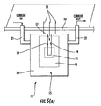
- FIG. 5(a) shows the current sensor of FIG. 1 sensing a current flowing on a printed circuit board.
- FIG. 5(b) is a depiction of a current sensor IC designed as an application specific integrated circuit (ASIC) comprising a Hall-effect or MR sensor coupled to an amplifier, according to an embodiment of the invention.
- ASIC application specific integrated circuit
- FIG. 1(a) shows a current sensor 10 according to an embodiment of the invention in a highly simplified illustration.
- the current sensor 10 comprises a magnetic field sensor 11 which is disposed on an optional support structure, such as a support plate 12.
- Magnetic field sensor 11 can generally comprises any magnetic field measuring technology, with or without an amplifier coupled to its output.
- magnetic field sensor 11 can be a Hall-effect sensor or a magnetoresistive (MR) sensor.
- An amplifier 31 is shown on support plate 12 and coupled to receive and amplify the electrical output signal provided by the magnetic field sensor 11.
- Hall effect sensors are based on the Hall effect which refers to the potential difference (Hall voltage) on the opposite sides of an electrical conductor (or semiconductor) through which an electric current is flowing, created by a magnetic field applied perpendicular to the direction of the current.
- a magnetoresistor (MR) is a well known device that changes its resistance in response to a change in the magnetic field. The magnetoresistive effect is known to be particularly large in permalloys, which are nickel-iron alloys, and other ferromagnetic materials.
- MR sensors are generally adapted for relatively low current sensing, while Hall-effect sensors are generally adapted for relatively higher level current sensing. MR sensors are known to have higher sensitivity and dynamic range as compared to Hall-effect sensors. If a MR sensor is used as sensor 11, it may be necessary to modify its mounting as known in the art.
- the magnetic field sensor 11 is at least partially surrounded by the primary conductor sandwich 13 which carries the current to be measured.
- the conductor sandwich 13 according to the present invention is generally arranged to make use of the physics property that in the center of an electrical conductor essentially no electromagnetic field can be build up from its own current.
- This inventive aspect effective eliminates the disadvantage described above based on current sensors disclosed in EP 1192473 / WO 00/79291 where the electromagnetic field associated with the current to be measured generates a magnetic field in the primary conductor, which can prevent precise measurement of the magnetic field associated with the current to be measured in the notch by adding another magnetic field component.
- This aspect of the present invention together with having the magnetic permeable layer 13(c) on the inside surface of a pair of electrical conductors 13(a) and 13(b) (shown in FIG. 1 (b) described below) protects the magnetic sensor from external (stray) magnetic fields by leading the stray fields away from the magnetic sensor generally resulting in significantly better sensor performance (e.g. linearity, accuracy), as compared to current sensors disclosed in EP1192473 / WO 00/79291 .
- Conductor sandwich 13 comprises an electrically conducting top layer 13(a) and electrically conducting bottom layer 13(b), having a layer of magnetic permeable material 13(c) interposed between.
- the thickness of magnetic permeable material 13(c) is generally more than an order of magnitude thinner as compared to the thickness of conducting top layer 13(a) and bottom layer 13(b).
- the electrically conducting top layer 13(a) and bottom layer 13(b) should be coupled together via a low resistance connection or be electrically common.
- the respective layers are secured to one another using an electrically conductive adhesive 28. Non-electrically conducting adhesives or other methods for securing the respective layers together may also be used.
- highly magnetic permeable materials generally provide a lower electrical conductivity as compared to the electrical conductivity of certain available low cost non-magnetic permeable materials, such as copper.
- the highly magnetic permeable material caries the current to be measured, such as disclosed in EP 1192473 / WO 00/79291 , the highly magnetic permeable material must be made thicker (and or wider) to obtain a required low impedance level.
- electrically conducting top and bottom layers 13(a) and 13(b) carry most of the current to be measured.
- electrically conducting top and bottom layers 13(a) and 13(b) are generally exclusive of magnetically permeable material.
- top and bottom conductor 13(a) and 13(b) absorb little of the magnetic field lines needed to measure the primary current.
- the current in current sensor 10 can thus be carried by relatively low cost highly electrically conducting generally non-magnetic permeable materials, such as copper.
- the thickness of the electrically conducting portions 13(a) and 13(b) of conductor sandwich 13 is generally on the order of 1 mm for 25 A of current, and the width of conductor sandwich 13 is generally about 5 to 40 mm, such as 10 to 20 mm.
- the overall thickness of the conductor sandwich 13 is generally 3 to 10 mm.
- the thickness of magnetic permeable material 13c is generally from 0.1 to 0.5 mm.
- Conductor sandwich 13 can have a strip-form design.
- the conductor sandwich 13 then surrounds the magnetic field sensor 11 in tubular fashion. It is also possible for this tubular arrangement of the conductor sandwich 13 to be closed at the top and/or bottom so that the conductor sandwich 13 surrounds the magnetic field sensor 11 in a cartridge-like or casing-like fashion.
- the magnetic field sensor 11 can be mounted in a plastic molding.
- the magnetic permeable material 13(c) of conductor sandwich 13 screens the magnetic field sensor 11 from extraneous magnetic and electric fields, while the electrically conducting portions 13a and 13(b) of conductor sandwich 13 provide electric field screening.
- conductor sandwich 13 provides screening from electric fields from various sources including primary side voltage peaks, as well as external magnetic fields which can arise from various sources.
- the conductor sandwich 13 also leads the magnetic field generated by the current to be measured through the magnetic field sensor 11.
- the magnetic permeable material 13c can be made from a variety of magnetic permeable materials.
- the term "magnetic permeable material” refers to a material that provides a permeability ( ⁇ ) of at least 500 ⁇ N/A 2 at 0.002 T and zero frequency.
- the magnetic permeable material 13(c) is generally an iron or a ferrous alloy.
- magnetic permeable material 13c comprises Mu-metal.
- Mu-metal is a nickel-iron alloy (75% nickel, 15% iron, plus copper and molybdenum) that has a very high magnetic permeability, about 25,000 ⁇ N/A 2 at 0.002 T and zero frequency.
- a high magnetic permeability layer 13(c) is generally effective at screening static or low-frequency magnetic fields.
- the magnetic permeable material 13(c) can also have a bimetallic configuration, in which case Mu-metal may be combined with one or more metals, such as copper, in amounts from 10 to about 70 wt %.
- FIG. 2 is a highly simplified diagram of the current sensor 10 of FIG. 1 in top view.
- Feature 21 corresponds to electrically conducting terminals the permits the sensor 10 to be connected to a current carrying line to be measured while terminals 22 provide the three terminal electrical output from sensor 11 which is generally required when sensor 11 is embodied as a Hall-effect sensor.
- the conductor sandwich 13 configured in accordance with the invention can be seen to have two gaps 16 and 17 which provide breaks in the electrical continuity between adjacent electrical conductor portions. Although gaps 16 and 17 are shown having a notch-like shape, other gap shapes can be used, including nonuniform shapes. A gap shown as a notch 16, 17 in each of two opposite portions 14, 15 of conductor sandwich 13, with the adjacent edges 18, 19 respectively, is shown in FIG. 2 .
- the magnetic field sensor 11 is shown positioned in the zone of the notch 17.
- the presence of the gaps, such as notches 16, 17, causes the current flowing through the conductor sandwich 13 to be led in a generally U-shaped path (see FIG. 3 ), and as a result the field lines of the magnetic field generated by the current to be measured being led through the magnetic field sensor 11.
- the conductor sandwich 13 therefore serves as forward and return electrical conductor. It is noted that the adjacent edges 18 and 19 may also overlap without physically touching one another other to also provide a gap. An overlapping arrangement is shown in FIG. 4(b) , as described below.
- FIG. 3 shows a current sensor 23 which basically corresponds to the current sensor 10 of Figs. 1 and 2 but has straight terminals 24. In other respects, the current sensor 23 generally corresponds to current sensor 10. The same reference numbers are therefore used for the same components.
- the arrow 25 shows how the current flowing through the conductor 13 is led in a generally U-shaped path. Although shown having an open end upon which the three (3) output terminals 22 emerge therefrom, the case can be enclosed (not shown) making provision not to short output terminals 22 together. It is possible to generally electrically short the electrically conducting top layer 13(a) and bottom layer 13(b), provided the shorting does not short across notches 16, 17 which would interrupt the desired generally U-shaped current pattern.
- FIG. 4(a) illustrates a current sensor 400 according to an embodiment of the present invention showing the pattern of magnetic field lines from primary conductor current 26 through the magnetic field sensor 11 and external stray magnetic field lines 29 being led away from the magnetic field sensor 11.
- the lowest magnetic resistance path is through the center around magnetic sensor 11.
- FIG. 4(b) shows a current sensor 450 according to another embodiment of the present invention having a primary conductor arrangement which provides overlapping conductor sandwich edges for enhanced immunity against external stray fields.
- An expanded view of the overlap arrangement is also provided.
- the overlapping arrangement together with the conductor sandwich 13 can avoid or at least help prevent saturation of the magnetically permeable material near the edges of conductor sandwich 13 and thus can provide improved linearity.
- the magnetic permeable layer 13(c) is recessed, and thus does not reach the surface of the conductor sandwich 13 at the edges of conductor sandwich 13.
- This arrangement provides protection for the magnetic permeable layer 13(c) from the magnetic field generated by the primary current.
- the edges of conductor sandwich 13 are rounded by end region which includes only electrically conductive layers 13(a) and 13(b).
- the distance between edge surface of conductor sandwich 13 and the edge of the magnetic permeable material 13(c) is at least equal to the thickness of one of the electrically conductive layers 13(a) and 13(b).
- FIG. 5(a) shows a current sensor 10 according to the invention in one of its applications of measuring the current carried by a conducting line on a printed circuit board (PCB) 20.
- PCB printed circuit board
- current sensor is generally soldered to PCB 20 and thus placed in series with one or more current carrying lines to be measured on PCB 20.
- the conductor sandwich 13 is shown contacting current carrying line on PCB 20 via conducting terminals 21.
- the sensor 10 is perpendicular to the plane of PCB 20.
- Electrical data signals (voltage) from current sensor 10 can be tapped via terminals 22 (3 terminals shown for a Hall-effect sensor) for further processing, such as for filtering and amplification.
- Sensors according to the present invention can also be formed on integrated circuit substrates, such as silicon, particularly for lower current sensing, such as milliamps up to several amps (e.g. up to 25 A).
- support structure 12 comprises an integrated circuit substrate having a semiconducting surface, such as a silicon substrate. Processing is performed such that the magnetic field sensor 11 is substantially surrounded by the multi-layer conductor sandwich 13 on all sides. Copper is currently commonly used as the metallization on modem integrated circuits which include a plurality of metallization levels, due to its relatively low cost, high electrically conductivity, and resistance to electromigration. Magnetic (ferric) materials are routinely deposited on integrated circuits for circuits such as Fe-RAMs.
- FIG. 5(b) shows a depiction of a current sensor IC 60 according to the present invention designed as an application specific integrated circuit (ASIC) comprising a Hall-effect or MR sensor 11 coupled to an amplifier 31 formed on a common substrate (e.g. substrate having a silicon surface) 12 and typically package in a single package, such as a plastic package.
- ASIC application specific integrated circuit
- controller 36 comprises an electric drive system controller for an automobile, such as for controlling motor and phase current in the electronic drive system of the automobile.
- the sensor IC can include both Hall-effect and MR-based sensors, with a switch for switching between the respective sensors based on a predetermined current level.
- the MR-based sensor is operable at lower current, while the Hall-effect sensor would be operable at higher current.
- the sensor signal could also be temperature compensated using known temperature sensor circuits (PTATs).
- the IC can also including a wireless transmitter and on-chip antenna for transmitting the detected signal to a remote monitoring location.
Landscapes
- Physics & Mathematics (AREA)
- General Physics & Mathematics (AREA)
- Condensed Matter Physics & Semiconductors (AREA)
- Measuring Instrument Details And Bridges, And Automatic Balancing Devices (AREA)
Claims (11)
- Stromsensor (10), welcher Folgendes umfasst:einen Magnetfeldsensor (11),eine Zwischenschichtanordnung (13), die einen Strom führt und eine elektrisch leitende obere Schicht (13(a)) und eine elektrisch leitende untere Schicht (13(b)) sowie eine Metallschicht, die ein zwischenstehend angeordnetes magnetisch permeables Material (13(c)) aufweist, umfasst, wobei jedes von dem magnetisch permeablen Material, der elektrisch leitenden oberen Schicht und der elektrisch leitenden unteren Schicht einen Teil des Stroms führt, wobei das magnetisch permeable Material (13(c)) um den Magnetfeldsensor (11) herum angeordnet ist, so dass der Magnetfeldsensor zumindest teilweise von dem magnetisch permeablen Material (13(c)) umgeben ist, und wobei die Zwischenschichtanordnung (13) mindestens einen Spalt (16, 17) zwischen benachbarten Rändern (18, 19) aufweist,wobei der Magnetfeldsensor (11) in der Nähe des Spalts (16, 17) angeordnet ist und bei der Verwendung magnetische Flusslinien, die sich aus dem in der Zwischenschichtanordnung fließenden Strom ergeben, operativ empfängt.
- Stromsensor nach Anspruch 1, wobei die angrenzenden Ränder (18, 19) einander überlappen.
- Stromsensor nach Anspruch 1, wobei der Magnetfeldsensor (11) zumindest teilweise über dem Spalt (16, 17) angeordnet ist.
- Stromsensor nach Anspruch 1, wobei die elektrisch leitende obere Schicht und die elektrisch leitende untere Schicht (13(a) und 13(b)) in erster Linie Kupfer umfassen.
- Stromsensor nach Anspruch 1, welcher ferner eine Tragstruktur (12) umfasst, wobei der Magnetfeldsensor (11) auf der Tragstruktur (12) angeordnet ist, wobei die Tragstruktur ein Substrat mit einer Halbleiteroberfläche umfasst, wobei der Stromsensor (60) ein auf der Halbleiteroberfläche gebildeter integrierter Stromsensor ist.
- Stromsensor nach Anspruch 5, welcher ferner einen auf der Halbleiteroberfläche ausgebildeten Verstärker (31) umfasst, der mit einem Ausgang des Magnetfeldsensors (11) gekoppelt ist.
- Steuersystem, welches Folgendes umfasst:einen Stromsensor (10) nach Anspruch 1 zum Bereitstellen eines Strommesssignals, das einen empfangenen Strom repräsentiert, undeine Steuereinrichtung (36), die gekoppelt ist, um das Strommesssignal zu empfangen und operativ gekoppelt ist, um mindestens ein weiteres System zu steuern.
- Steuersystem nach Anspruch 7, wobei das weitere System einen elektronischen Antrieb für ein Automobil umfasst und die Steuereinrichtung (36) eine Steuereinrichtung für ein elektrisches Antriebssystem umfasst.
- Steuersystem nach Anspruch 7, welches ferner eine Tragstruktur (12) umfasst, wobei der Magnetfeldsensor (11) des Stromsensors (10) auf der Tragstruktur (12) angeordnet ist, wobei die Tragstruktur ein Substrat mit einer Halbleiteroberfläche umfasst und wobei der Stromsensor ein auf der Halbleiteroberfläche ausgebildeter integrierter Stromsensor (60) ist.
- Steuersystem nach Anspruch 9, welches ferner einen auf der Halbleiteroberfläche ausgebildeten Verstärker (31) umfasst, der mit einem Ausgang des Magnetfeldsensors (11) gekoppelt ist.
- Steuersystem nach Anspruch 7, wobei der Magnetfeldsensor (11) einen Hall-Effekt-Sensor umfasst.
Applications Claiming Priority (3)
| Application Number | Priority Date | Filing Date | Title |
|---|---|---|---|
| US95210507P | 2007-07-26 | 2007-07-26 | |
| US11/851,981 US7612553B2 (en) | 2007-07-26 | 2007-09-07 | Current sensor having sandwiched magnetic permeability layer |
| PCT/US2008/070950 WO2009015250A1 (en) | 2007-07-26 | 2008-07-24 | Current sensor having sandwiched magnetic permeability layer |
Publications (3)
| Publication Number | Publication Date |
|---|---|
| EP2174152A1 EP2174152A1 (de) | 2010-04-14 |
| EP2174152A4 EP2174152A4 (de) | 2012-11-07 |
| EP2174152B1 true EP2174152B1 (de) | 2013-12-11 |
Family
ID=40281816
Family Applications (1)
| Application Number | Title | Priority Date | Filing Date |
|---|---|---|---|
| EP08826498.1A Not-in-force EP2174152B1 (de) | 2007-07-26 | 2008-07-24 | Stromsensor mit zwischenangeordneter schicht für magnetische permeabilität |
Country Status (4)
| Country | Link |
|---|---|
| US (1) | US7612553B2 (de) |
| EP (1) | EP2174152B1 (de) |
| CN (1) | CN101809457B (de) |
| WO (1) | WO2009015250A1 (de) |
Families Citing this family (22)
| Publication number | Priority date | Publication date | Assignee | Title |
|---|---|---|---|---|
| JP5366418B2 (ja) * | 2008-03-24 | 2013-12-11 | 東光東芝メーターシステムズ株式会社 | 電流検出器およびこれを用いた電力量計 |
| US20090265041A1 (en) * | 2008-04-18 | 2009-10-22 | Benjamin Daniel E | Power Distribution and Monitoring System |
| US7642768B1 (en) * | 2008-10-21 | 2010-01-05 | Honeywell International Inc. | Current sensor having field screening arrangement including electrical conductors sandwiching magnetic permeability layer |
| DE102008061006A1 (de) * | 2008-11-28 | 2010-06-02 | Esw Gmbh | Verfahren und Vorrichtung zur Messung von elektrischen Strom |
| US8203328B2 (en) * | 2009-03-12 | 2012-06-19 | Consolidated Edison Company Of New York, Inc. | Current measuring device |
| JP5657570B2 (ja) * | 2009-12-28 | 2015-01-21 | Tdk株式会社 | 磁界検出装置 |
| US8760149B2 (en) * | 2010-04-08 | 2014-06-24 | Infineon Technologies Ag | Magnetic field current sensors |
| US9121885B2 (en) * | 2010-08-16 | 2015-09-01 | Infineon Technologies Ag | Sensor package and method of manufacturing thereof |
| FR2976765B1 (fr) * | 2011-06-20 | 2015-05-01 | Renault Sa | Dispositif pour proteger un espace a proximite d'une source magnetique et procede de fabrication d'un tel dispositif |
| US8952686B2 (en) | 2011-10-25 | 2015-02-10 | Honeywell International Inc. | High current range magnetoresistive-based current sensor |
| US9322632B2 (en) | 2011-12-05 | 2016-04-26 | Gm Global Technology Operations Inc. | Linear position sensor assembly having magnetic shield |
| US9001476B2 (en) * | 2013-03-15 | 2015-04-07 | Rockwell Automation Technologies, Inc. | Multimotor variable frequency overload |
| CH708052B1 (de) * | 2013-05-07 | 2016-09-15 | Melexis Technologies Nv | Vorrichtung zur Strommessung. |
| CN203809329U (zh) * | 2014-04-14 | 2014-09-03 | 江苏多维科技有限公司 | 一种直流风扇控制芯片 |
| CN106461706B (zh) * | 2014-06-20 | 2019-07-12 | 日立汽车系统株式会社 | 电流检测装置 |
| CN107076784B (zh) * | 2014-12-15 | 2019-06-14 | 株式会社村田制作所 | 电流传感器 |
| DE102015218290A1 (de) * | 2015-09-23 | 2017-03-23 | Zf Friedrichshafen Ag | Vorrichtung für Hoch-/Mittel-/Niederspannungsstrommessung |
| DE102015223088A1 (de) * | 2015-11-23 | 2017-05-24 | Zf Friedrichshafen Ag | Einrichtung zur Messung hoher und mittlerer Hochspannungsströme |
| US11619658B2 (en) | 2017-12-08 | 2023-04-04 | Texas Instruments Incorporated | Semiconductor integrated fluxgate device shielded by discrete magnetic plate |
| DE102018204366A1 (de) * | 2018-03-22 | 2019-09-26 | Robert Bosch Gmbh | Induktives Bauelement und Hochfrequenz-Filtervorrichtung |
| JP7243747B2 (ja) * | 2021-01-29 | 2023-03-22 | Tdk株式会社 | 電流センサおよびそれを備えた電気制御装置 |
| DE102021114943A1 (de) | 2021-06-10 | 2022-12-15 | Infineon Technologies Ag | Sensorvorrichtungen mit Weichmagneten und zugehörige Herstellungsverfahren |
Family Cites Families (34)
| Publication number | Priority date | Publication date | Assignee | Title |
|---|---|---|---|---|
| US2678357A (en) * | 1951-03-27 | 1954-05-11 | Bell & Howell Co | Magnetic sound and combined optical and magnetic sound translating apparatus |
| US3436650A (en) * | 1965-09-30 | 1969-04-01 | Us Navy | Spinning line integral magnetometer for measuring a current or an electric field |
| CH650357A5 (de) | 1981-03-26 | 1985-07-15 | Landis & Gyr Ag | Magnetkernloser messwandler zum potentialfreien messen eines messstromes. |
| DE3479758D1 (en) | 1984-01-07 | 1989-10-19 | Duerrwaechter E Dr Doduco | Device for measuring electrical currents using a magnetic-field sensor |
| JPS60214404A (ja) | 1984-04-10 | 1985-10-26 | Nec Corp | 磁気ヘツドシ−ルド |
| US4687987A (en) | 1984-09-28 | 1987-08-18 | The United States Of America As Represented By The United States Department Of Energy | Beam current sensor |
| US4894610A (en) | 1985-09-14 | 1990-01-16 | LOZ Landis & Gyr Zug AG | Current-transformer arrangement for an electrostatic meter |
| US4890083A (en) | 1988-10-20 | 1989-12-26 | Texas Instruments Incorporated | Shielding material and shielded room |
| US5017859A (en) * | 1989-08-03 | 1991-05-21 | Westinghouse Electric Corp. | Integral capacitive divider bus bar voltage measuring apparatus and combined current sensor |
| FR2678069A1 (fr) | 1991-06-18 | 1992-12-24 | Commissariat Energie Atomique | Capteur de courant utilisant un magnetometre directionnel a resonance. |
| US5642041A (en) | 1994-11-21 | 1997-06-24 | General Electric Company | Alternating current sensor employing parallel plates and having high dynamic range and accuracy |
| JP3007553B2 (ja) | 1995-03-24 | 2000-02-07 | 日本レム株式会社 | 電流センサ |
| DE19549181A1 (de) | 1995-12-30 | 1997-07-03 | Bosch Gmbh Robert | Vorrichtung zur Messung eines in einem Leiter fließenden Stromes |
| US5694103A (en) * | 1996-04-25 | 1997-12-02 | Schlumberger Industries, Inc. | Laminated figure 8 power meter core |
| US5831424A (en) | 1996-05-01 | 1998-11-03 | Southwest Research Institute | Isolated current sensor |
| DE19741417B4 (de) | 1997-09-19 | 2004-02-26 | Klaus Bruchmann | Strommessgerät mit Hallsensor |
| CH692260A5 (fr) | 1998-01-28 | 2002-04-15 | Lem Liaisons Electron Mec | Dispositif d'alimentation en courant muni d'un capteur de courant. |
| DE19928399B4 (de) | 1999-06-22 | 2004-07-08 | Honeywell Ag | Stromsensor |
| US7090636B2 (en) * | 2000-03-31 | 2006-08-15 | Fe Rx Incorporated | Permanent magnet keeper-shield assembly |
| GB0029953D0 (en) | 2000-12-07 | 2001-01-24 | Lem Heme Ltd | Current sensor |
| EP1273921A1 (de) * | 2001-07-06 | 2003-01-08 | Sanken Electric Co., Ltd. | Hall-Effekt-Stromdetektor |
| EP1281974B1 (de) * | 2001-07-06 | 2007-04-18 | Sanken Electric Co., Ltd. | Hall-Effekt-Stromdetektor |
| CN1295514C (zh) * | 2001-11-01 | 2007-01-17 | 旭化成电子材料元件株式会社 | 电流传感器与电流传感器的制造方法 |
| AU2002349497A1 (en) * | 2001-11-26 | 2003-06-10 | Asahi Kasei Electronics Co., Ltd. | Current sensor |
| US20040008022A1 (en) | 2002-07-11 | 2004-01-15 | Viola Jeffrey L. | Current sensor |
| US6963182B2 (en) * | 2002-11-29 | 2005-11-08 | Toyoda Koki Kabushiki Kaisha | Motor control device and motor control method |
| USD505870S1 (en) | 2003-01-07 | 2005-06-07 | Liaisons-Electroniques Mecaniques Lem S.A. | Current sensor |
| JP4332623B2 (ja) | 2003-02-26 | 2009-09-16 | テクトロニクス・インコーポレイテッド | 電流プローブ |
| JP4247821B2 (ja) | 2003-04-11 | 2009-04-02 | キヤノン電子株式会社 | 電流センサ |
| WO2005033716A1 (en) | 2003-10-01 | 2005-04-14 | Eaton Corporation | System and method for current sensing using anti-differential, error correcting current sensing |
| US7164263B2 (en) | 2004-01-16 | 2007-01-16 | Fieldmetrics, Inc. | Current sensor |
| USD510881S1 (en) | 2004-06-01 | 2005-10-25 | Liaisons Electroniques-Mecaniques Lem S.A. | Electrical current sensor |
| KR20050055066A (ko) * | 2004-07-14 | 2005-06-10 | (주)에이티에스네트웍스 | 직류 전류 센서 |
| US7298132B2 (en) * | 2005-04-13 | 2007-11-20 | Crane Co. | Current sensor |
-
2007
- 2007-09-07 US US11/851,981 patent/US7612553B2/en not_active Expired - Fee Related
-
2008
- 2008-07-24 EP EP08826498.1A patent/EP2174152B1/de not_active Not-in-force
- 2008-07-24 WO PCT/US2008/070950 patent/WO2009015250A1/en not_active Ceased
- 2008-07-24 CN CN200880109323.7A patent/CN101809457B/zh not_active Expired - Fee Related
Also Published As
| Publication number | Publication date |
|---|---|
| US20090027047A1 (en) | 2009-01-29 |
| WO2009015250A1 (en) | 2009-01-29 |
| US7612553B2 (en) | 2009-11-03 |
| CN101809457B (zh) | 2014-03-26 |
| CN101809457A (zh) | 2010-08-18 |
| EP2174152A4 (de) | 2012-11-07 |
| EP2174152A1 (de) | 2010-04-14 |
Similar Documents
| Publication | Publication Date | Title |
|---|---|---|
| US7612553B2 (en) | Current sensor having sandwiched magnetic permeability layer | |
| US7642768B1 (en) | Current sensor having field screening arrangement including electrical conductors sandwiching magnetic permeability layer | |
| US7106046B2 (en) | Current measuring method and current measuring device | |
| EP1107328B1 (de) | Stromdetektor mit einer Hall-Effekt-Anordnung | |
| EP2442118B1 (de) | Magnetisch ausbalancierter stromsensor | |
| EP1965217B1 (de) | Stromsensor mit offenem Regelkreis und hoher Bandbreite | |
| US9372240B2 (en) | Current sensor | |
| US9547024B2 (en) | Device for current measurement | |
| EP1107327A2 (de) | Rauscharmer Halbleiterstromdetektor | |
| US10670671B2 (en) | Magnetic field sensor circuit in package with means to add a signal from a coil | |
| EP3779490A1 (de) | Magnetischer sensor | |
| JPWO2018100778A1 (ja) | 電流センサ及び電流センサユニット | |
| US11994541B2 (en) | Current sensor assemblies for low currents | |
| US20240295586A1 (en) | Magnetic sensor and electronic device | |
| WO2015075623A1 (en) | Power module comprising an integrated current measurement | |
| JP6384677B2 (ja) | 電流センサ | |
| CN113311370A (zh) | 磁性传感器及磁性检测方法 | |
| CN108780130B (zh) | 磁传感器 | |
| EP4043890B1 (de) | Magnetischer sensor und stromerfassungsvorrichtung damit |
Legal Events
| Date | Code | Title | Description |
|---|---|---|---|
| PUAI | Public reference made under article 153(3) epc to a published international application that has entered the european phase |
Free format text: ORIGINAL CODE: 0009012 |
|
| 17P | Request for examination filed |
Effective date: 20100122 |
|
| AK | Designated contracting states |
Kind code of ref document: A1 Designated state(s): AT BE BG CH CY CZ DE DK EE ES FI FR GB GR HR HU IE IS IT LI LT LU LV MC MT NL NO PL PT RO SE SI SK TR |
|
| AX | Request for extension of the european patent |
Extension state: AL BA MK RS |
|
| DAX | Request for extension of the european patent (deleted) | ||
| REG | Reference to a national code |
Ref country code: DE Ref legal event code: R079 Ref document number: 602008029287 Country of ref document: DE Free format text: PREVIOUS MAIN CLASS: G01R0033000000 Ipc: G01R0033070000 |
|
| A4 | Supplementary search report drawn up and despatched |
Effective date: 20121008 |
|
| RIC1 | Information provided on ipc code assigned before grant |
Ipc: G01R 15/20 20060101ALI20121001BHEP Ipc: G01R 33/07 20060101AFI20121001BHEP |
|
| 17Q | First examination report despatched |
Effective date: 20121023 |
|
| GRAP | Despatch of communication of intention to grant a patent |
Free format text: ORIGINAL CODE: EPIDOSNIGR1 |
|
| INTG | Intention to grant announced |
Effective date: 20130725 |
|
| GRAS | Grant fee paid |
Free format text: ORIGINAL CODE: EPIDOSNIGR3 |
|
| GRAA | (expected) grant |
Free format text: ORIGINAL CODE: 0009210 |
|
| AK | Designated contracting states |
Kind code of ref document: B1 Designated state(s): AT BE BG CH CY CZ DE DK EE ES FI FR GB GR HR HU IE IS IT LI LT LU LV MC MT NL NO PL PT RO SE SI SK TR |
|
| REG | Reference to a national code |
Ref country code: GB Ref legal event code: FG4D |
|
| REG | Reference to a national code |
Ref country code: CH Ref legal event code: EP |
|
| REG | Reference to a national code |
Ref country code: AT Ref legal event code: REF Ref document number: 644854 Country of ref document: AT Kind code of ref document: T Effective date: 20140115 |
|
| REG | Reference to a national code |
Ref country code: IE Ref legal event code: FG4D |
|
| REG | Reference to a national code |
Ref country code: DE Ref legal event code: R096 Ref document number: 602008029287 Country of ref document: DE Effective date: 20140206 |
|
| REG | Reference to a national code |
Ref country code: NL Ref legal event code: VDEP Effective date: 20131211 |
|
| REG | Reference to a national code |
Ref country code: AT Ref legal event code: MK05 Ref document number: 644854 Country of ref document: AT Kind code of ref document: T Effective date: 20131211 |
|
| PG25 | Lapsed in a contracting state [announced via postgrant information from national office to epo] |
Ref country code: SE Free format text: LAPSE BECAUSE OF FAILURE TO SUBMIT A TRANSLATION OF THE DESCRIPTION OR TO PAY THE FEE WITHIN THE PRESCRIBED TIME-LIMIT Effective date: 20131211 Ref country code: NO Free format text: LAPSE BECAUSE OF FAILURE TO SUBMIT A TRANSLATION OF THE DESCRIPTION OR TO PAY THE FEE WITHIN THE PRESCRIBED TIME-LIMIT Effective date: 20140311 Ref country code: LT Free format text: LAPSE BECAUSE OF FAILURE TO SUBMIT A TRANSLATION OF THE DESCRIPTION OR TO PAY THE FEE WITHIN THE PRESCRIBED TIME-LIMIT Effective date: 20131211 Ref country code: HR Free format text: LAPSE BECAUSE OF FAILURE TO SUBMIT A TRANSLATION OF THE DESCRIPTION OR TO PAY THE FEE WITHIN THE PRESCRIBED TIME-LIMIT Effective date: 20131211 Ref country code: FI Free format text: LAPSE BECAUSE OF FAILURE TO SUBMIT A TRANSLATION OF THE DESCRIPTION OR TO PAY THE FEE WITHIN THE PRESCRIBED TIME-LIMIT Effective date: 20131211 Ref country code: NL Free format text: LAPSE BECAUSE OF FAILURE TO SUBMIT A TRANSLATION OF THE DESCRIPTION OR TO PAY THE FEE WITHIN THE PRESCRIBED TIME-LIMIT Effective date: 20131211 |
|
| REG | Reference to a national code |
Ref country code: LT Ref legal event code: MG4D |
|
| PG25 | Lapsed in a contracting state [announced via postgrant information from national office to epo] |
Ref country code: AT Free format text: LAPSE BECAUSE OF FAILURE TO SUBMIT A TRANSLATION OF THE DESCRIPTION OR TO PAY THE FEE WITHIN THE PRESCRIBED TIME-LIMIT Effective date: 20131211 Ref country code: CY Free format text: LAPSE BECAUSE OF FAILURE TO SUBMIT A TRANSLATION OF THE DESCRIPTION OR TO PAY THE FEE WITHIN THE PRESCRIBED TIME-LIMIT Effective date: 20131211 Ref country code: LV Free format text: LAPSE BECAUSE OF FAILURE TO SUBMIT A TRANSLATION OF THE DESCRIPTION OR TO PAY THE FEE WITHIN THE PRESCRIBED TIME-LIMIT Effective date: 20131211 |
|
| PG25 | Lapsed in a contracting state [announced via postgrant information from national office to epo] |
Ref country code: BE Free format text: LAPSE BECAUSE OF FAILURE TO SUBMIT A TRANSLATION OF THE DESCRIPTION OR TO PAY THE FEE WITHIN THE PRESCRIBED TIME-LIMIT Effective date: 20131211 Ref country code: EE Free format text: LAPSE BECAUSE OF FAILURE TO SUBMIT A TRANSLATION OF THE DESCRIPTION OR TO PAY THE FEE WITHIN THE PRESCRIBED TIME-LIMIT Effective date: 20131211 Ref country code: IS Free format text: LAPSE BECAUSE OF FAILURE TO SUBMIT A TRANSLATION OF THE DESCRIPTION OR TO PAY THE FEE WITHIN THE PRESCRIBED TIME-LIMIT Effective date: 20140411 |
|
| PG25 | Lapsed in a contracting state [announced via postgrant information from national office to epo] |
Ref country code: PT Free format text: LAPSE BECAUSE OF FAILURE TO SUBMIT A TRANSLATION OF THE DESCRIPTION OR TO PAY THE FEE WITHIN THE PRESCRIBED TIME-LIMIT Effective date: 20140411 Ref country code: SK Free format text: LAPSE BECAUSE OF FAILURE TO SUBMIT A TRANSLATION OF THE DESCRIPTION OR TO PAY THE FEE WITHIN THE PRESCRIBED TIME-LIMIT Effective date: 20131211 Ref country code: RO Free format text: LAPSE BECAUSE OF FAILURE TO SUBMIT A TRANSLATION OF THE DESCRIPTION OR TO PAY THE FEE WITHIN THE PRESCRIBED TIME-LIMIT Effective date: 20131211 Ref country code: CZ Free format text: LAPSE BECAUSE OF FAILURE TO SUBMIT A TRANSLATION OF THE DESCRIPTION OR TO PAY THE FEE WITHIN THE PRESCRIBED TIME-LIMIT Effective date: 20131211 Ref country code: ES Free format text: LAPSE BECAUSE OF FAILURE TO SUBMIT A TRANSLATION OF THE DESCRIPTION OR TO PAY THE FEE WITHIN THE PRESCRIBED TIME-LIMIT Effective date: 20131211 Ref country code: PL Free format text: LAPSE BECAUSE OF FAILURE TO SUBMIT A TRANSLATION OF THE DESCRIPTION OR TO PAY THE FEE WITHIN THE PRESCRIBED TIME-LIMIT Effective date: 20131211 |
|
| REG | Reference to a national code |
Ref country code: DE Ref legal event code: R097 Ref document number: 602008029287 Country of ref document: DE |
|
| PLBE | No opposition filed within time limit |
Free format text: ORIGINAL CODE: 0009261 |
|
| STAA | Information on the status of an ep patent application or granted ep patent |
Free format text: STATUS: NO OPPOSITION FILED WITHIN TIME LIMIT |
|
| PG25 | Lapsed in a contracting state [announced via postgrant information from national office to epo] |
Ref country code: DK Free format text: LAPSE BECAUSE OF FAILURE TO SUBMIT A TRANSLATION OF THE DESCRIPTION OR TO PAY THE FEE WITHIN THE PRESCRIBED TIME-LIMIT Effective date: 20131211 |
|
| 26N | No opposition filed |
Effective date: 20140912 |
|
| REG | Reference to a national code |
Ref country code: DE Ref legal event code: R097 Ref document number: 602008029287 Country of ref document: DE Effective date: 20140912 |
|
| PG25 | Lapsed in a contracting state [announced via postgrant information from national office to epo] |
Ref country code: SI Free format text: LAPSE BECAUSE OF FAILURE TO SUBMIT A TRANSLATION OF THE DESCRIPTION OR TO PAY THE FEE WITHIN THE PRESCRIBED TIME-LIMIT Effective date: 20131211 Ref country code: LU Free format text: LAPSE BECAUSE OF FAILURE TO SUBMIT A TRANSLATION OF THE DESCRIPTION OR TO PAY THE FEE WITHIN THE PRESCRIBED TIME-LIMIT Effective date: 20140724 |
|
| REG | Reference to a national code |
Ref country code: CH Ref legal event code: PL |
|
| REG | Reference to a national code |
Ref country code: IE Ref legal event code: MM4A |
|
| PG25 | Lapsed in a contracting state [announced via postgrant information from national office to epo] |
Ref country code: CH Free format text: LAPSE BECAUSE OF NON-PAYMENT OF DUE FEES Effective date: 20140731 Ref country code: LI Free format text: LAPSE BECAUSE OF NON-PAYMENT OF DUE FEES Effective date: 20140731 |
|
| PG25 | Lapsed in a contracting state [announced via postgrant information from national office to epo] |
Ref country code: IE Free format text: LAPSE BECAUSE OF NON-PAYMENT OF DUE FEES Effective date: 20140724 |
|
| PG25 | Lapsed in a contracting state [announced via postgrant information from national office to epo] |
Ref country code: MC Free format text: LAPSE BECAUSE OF FAILURE TO SUBMIT A TRANSLATION OF THE DESCRIPTION OR TO PAY THE FEE WITHIN THE PRESCRIBED TIME-LIMIT Effective date: 20131211 |
|
| PG25 | Lapsed in a contracting state [announced via postgrant information from national office to epo] |
Ref country code: BG Free format text: LAPSE BECAUSE OF FAILURE TO SUBMIT A TRANSLATION OF THE DESCRIPTION OR TO PAY THE FEE WITHIN THE PRESCRIBED TIME-LIMIT Effective date: 20131211 |
|
| REG | Reference to a national code |
Ref country code: FR Ref legal event code: PLFP Year of fee payment: 9 |
|
| PG25 | Lapsed in a contracting state [announced via postgrant information from national office to epo] |
Ref country code: MT Free format text: LAPSE BECAUSE OF FAILURE TO SUBMIT A TRANSLATION OF THE DESCRIPTION OR TO PAY THE FEE WITHIN THE PRESCRIBED TIME-LIMIT Effective date: 20131211 Ref country code: GR Free format text: LAPSE BECAUSE OF FAILURE TO SUBMIT A TRANSLATION OF THE DESCRIPTION OR TO PAY THE FEE WITHIN THE PRESCRIBED TIME-LIMIT Effective date: 20140312 Ref country code: IT Free format text: LAPSE BECAUSE OF FAILURE TO SUBMIT A TRANSLATION OF THE DESCRIPTION OR TO PAY THE FEE WITHIN THE PRESCRIBED TIME-LIMIT Effective date: 20131211 |
|
| PG25 | Lapsed in a contracting state [announced via postgrant information from national office to epo] |
Ref country code: TR Free format text: LAPSE BECAUSE OF FAILURE TO SUBMIT A TRANSLATION OF THE DESCRIPTION OR TO PAY THE FEE WITHIN THE PRESCRIBED TIME-LIMIT Effective date: 20131211 Ref country code: HU Free format text: LAPSE BECAUSE OF FAILURE TO SUBMIT A TRANSLATION OF THE DESCRIPTION OR TO PAY THE FEE WITHIN THE PRESCRIBED TIME-LIMIT; INVALID AB INITIO Effective date: 20080724 |
|
| REG | Reference to a national code |
Ref country code: FR Ref legal event code: PLFP Year of fee payment: 10 |
|
| REG | Reference to a national code |
Ref country code: FR Ref legal event code: PLFP Year of fee payment: 11 |
|
| PGFP | Annual fee paid to national office [announced via postgrant information from national office to epo] |
Ref country code: FR Payment date: 20180726 Year of fee payment: 11 |
|
| PG25 | Lapsed in a contracting state [announced via postgrant information from national office to epo] |
Ref country code: FR Free format text: LAPSE BECAUSE OF NON-PAYMENT OF DUE FEES Effective date: 20190731 |
|
| PGFP | Annual fee paid to national office [announced via postgrant information from national office to epo] |
Ref country code: GB Payment date: 20200724 Year of fee payment: 13 Ref country code: DE Payment date: 20200729 Year of fee payment: 13 |
|
| REG | Reference to a national code |
Ref country code: DE Ref legal event code: R119 Ref document number: 602008029287 Country of ref document: DE |
|
| GBPC | Gb: european patent ceased through non-payment of renewal fee |
Effective date: 20210724 |
|
| PG25 | Lapsed in a contracting state [announced via postgrant information from national office to epo] |
Ref country code: GB Free format text: LAPSE BECAUSE OF NON-PAYMENT OF DUE FEES Effective date: 20210724 Ref country code: DE Free format text: LAPSE BECAUSE OF NON-PAYMENT OF DUE FEES Effective date: 20220201 |