EP2015562A1 - Verarbeitungsvorrichtung zum Korrigieren fehlerhafter Pixelwerte eines Bildsensors, Bildsensor mit der Verarbeitungsvorrichtung sowie Verfahren - Google Patents
Verarbeitungsvorrichtung zum Korrigieren fehlerhafter Pixelwerte eines Bildsensors, Bildsensor mit der Verarbeitungsvorrichtung sowie Verfahren Download PDFInfo
- Publication number
- EP2015562A1 EP2015562A1 EP07301218A EP07301218A EP2015562A1 EP 2015562 A1 EP2015562 A1 EP 2015562A1 EP 07301218 A EP07301218 A EP 07301218A EP 07301218 A EP07301218 A EP 07301218A EP 2015562 A1 EP2015562 A1 EP 2015562A1
- Authority
- EP
- European Patent Office
- Prior art keywords
- pixel
- values
- value
- defect
- image sensor
- Prior art date
- Legal status (The legal status is an assumption and is not a legal conclusion. Google has not performed a legal analysis and makes no representation as to the accuracy of the status listed.)
- Withdrawn
Links
- 230000007547 defect Effects 0.000 title claims abstract description 71
- 238000000034 method Methods 0.000 title claims description 15
- 238000012545 processing Methods 0.000 title abstract description 34
- 238000003491 array Methods 0.000 claims description 22
- 238000010586 diagram Methods 0.000 description 12
- 238000012937 correction Methods 0.000 description 7
- 238000005516 engineering process Methods 0.000 description 5
- 230000014509 gene expression Effects 0.000 description 4
- 238000004519 manufacturing process Methods 0.000 description 4
- 238000004364 calculation method Methods 0.000 description 3
- 238000009826 distribution Methods 0.000 description 3
- 241000519995 Stachys sylvatica Species 0.000 description 2
- 230000004397 blinking Effects 0.000 description 2
- 230000002950 deficient Effects 0.000 description 2
- 238000011156 evaluation Methods 0.000 description 2
- 239000002245 particle Substances 0.000 description 2
- 238000003892 spreading Methods 0.000 description 2
- 239000003086 colorant Substances 0.000 description 1
- 230000001419 dependent effect Effects 0.000 description 1
- 238000011161 development Methods 0.000 description 1
- 230000000694 effects Effects 0.000 description 1
- 230000010354 integration Effects 0.000 description 1
- 238000012805 post-processing Methods 0.000 description 1
Images


Classifications
-
- H—ELECTRICITY
- H04—ELECTRIC COMMUNICATION TECHNIQUE
- H04N—PICTORIAL COMMUNICATION, e.g. TELEVISION
- H04N25/00—Circuitry of solid-state image sensors [SSIS]; Control thereof
- H04N25/60—Noise processing, e.g. detecting, correcting, reducing or removing noise
- H04N25/68—Noise processing, e.g. detecting, correcting, reducing or removing noise applied to defects
- H04N25/683—Noise processing, e.g. detecting, correcting, reducing or removing noise applied to defects by defect estimation performed on the scene signal, e.g. real time or on the fly detection
-
- H—ELECTRICITY
- H04—ELECTRIC COMMUNICATION TECHNIQUE
- H04N—PICTORIAL COMMUNICATION, e.g. TELEVISION
- H04N23/00—Cameras or camera modules comprising electronic image sensors; Control thereof
- H04N23/10—Cameras or camera modules comprising electronic image sensors; Control thereof for generating image signals from different wavelengths
- H04N23/13—Cameras or camera modules comprising electronic image sensors; Control thereof for generating image signals from different wavelengths with multiple sensors
-
- H—ELECTRICITY
- H04—ELECTRIC COMMUNICATION TECHNIQUE
- H04N—PICTORIAL COMMUNICATION, e.g. TELEVISION
- H04N23/00—Cameras or camera modules comprising electronic image sensors; Control thereof
- H04N23/80—Camera processing pipelines; Components thereof
- H04N23/84—Camera processing pipelines; Components thereof for processing colour signals
- H04N23/843—Demosaicing, e.g. interpolating colour pixel values
-
- H—ELECTRICITY
- H04—ELECTRIC COMMUNICATION TECHNIQUE
- H04N—PICTORIAL COMMUNICATION, e.g. TELEVISION
- H04N25/00—Circuitry of solid-state image sensors [SSIS]; Control thereof
- H04N25/60—Noise processing, e.g. detecting, correcting, reducing or removing noise
- H04N25/68—Noise processing, e.g. detecting, correcting, reducing or removing noise applied to defects
-
- H—ELECTRICITY
- H04—ELECTRIC COMMUNICATION TECHNIQUE
- H04N—PICTORIAL COMMUNICATION, e.g. TELEVISION
- H04N25/00—Circuitry of solid-state image sensors [SSIS]; Control thereof
- H04N25/70—SSIS architectures; Circuits associated therewith
-
- H—ELECTRICITY
- H04—ELECTRIC COMMUNICATION TECHNIQUE
- H04N—PICTORIAL COMMUNICATION, e.g. TELEVISION
- H04N25/00—Circuitry of solid-state image sensors [SSIS]; Control thereof
- H04N25/70—SSIS architectures; Circuits associated therewith
- H04N25/76—Addressed sensors, e.g. MOS or CMOS sensors
-
- H—ELECTRICITY
- H04—ELECTRIC COMMUNICATION TECHNIQUE
- H04N—PICTORIAL COMMUNICATION, e.g. TELEVISION
- H04N2209/00—Details of colour television systems
- H04N2209/04—Picture signal generators
- H04N2209/041—Picture signal generators using solid-state devices
- H04N2209/048—Picture signal generators using solid-state devices having several pick-up sensors
- H04N2209/049—Picture signal generators using solid-state devices having several pick-up sensors having three pick-up sensors
Definitions
- the invention relates to a processing device for correcting defect pixel values of an image sensor unit, the image sensor unit and a respective method and, more specifically, to a processing device for correcting of at least one defect pixel value of an image sensor, the image sensor comprising at least a first and a second pixel array, wherein the image sensor unit is embodied to project the same image onto each pixel array, the processing device comprising at least a first and a second input channel for receiving pixel values of the first and the second pixel array, respectively, wherein the processing device is operable to exchange the defect pixel value by a corrected pixel value, wherein the corrected pixel value is estimated by evaluating the values of neighbouring pixels of the defect pixel of the same pixel array, and to the said image sensor and the method.
- Image sensors comprise one or more pixel arrays on which an image is projected. For grey-scale images sensors (black-and-white image sensors) one pixel array is sufficient. Colour image sensors usually require more than one pixel array, more precisely, they usually require three pixel arrays, whereby each pixel array is responsible for receiving the information of a colour component of the image. In this connection 3-chip image sensors are known having one chip per colour, whereby the spread of the original incoming image towards these three chips is done by means of prisms and colour filters.
- CMOS-sensor which can be produced in the standard CMOS process, which allows integrating on a single chip also other circuits, such as analogue to digital converters (ADC), digital controller for read-out from the CMOS-sensor and sometimes also digital signal processing cores for signal post-processing.
- ADC analogue to digital converters
- CMOS image sensors use low supply voltages and that they can be fabricated at low cost due to the possible integration of the other circuits on one single chip.
- CMOS image sensors are often suffering from fixed pattern noise and random defect pixels, whereby the pixel defects in an imager are seen as spot noise.
- the white spots on a dark portion of the image are due to pixels with excessive leakage current and the dark spots on a white portion of the image due to either a particle covering the pixel or a defect in the pixel electronics causing the pixel to be insensitive.
- Defect pixels are mainly created during manufacturing, some more can occur with time. This spot noise strongly degrades image quality.
- some random defective pixels are usually accepted even for professional devices. In this case, the defect pixels are corrected by signal processing.
- a processing device which is capable to correct at least one defect pixel value of an image sensor unit.
- the processing device allows to correct the values of especially bonded or clustered areas of defect pixels, but it is preferred that the processing device is embodied to correct a bonded area with only one single defect pixel as sensor units with larger clustered areas of defect pixels are preferably sorted out during fabrication.
- the image sensor unit is of based on any technology like CMOS or CCD and comprises at least two two-dimensional pixel arrays for sensing impinging light, the pixel arrays being arranged on one or more chips.
- the image sensor unit is realised so that an incoming image is projected in parallel onto the at least two pixel arrays, wherein the at least two pixel areas receive the same spatial image sections.
- image is herein used as a two-dimensional array of light intensity and may be but is not restricted to a real image.
- the processing device shows corresponding to the at least two pixel arrays a respective number of input channels for receiving the read-out values from the at least two pixel arrays.
- the processing device is adapted to exchange the at least one defect pixel by a corrected value in order to correct the defect pixel value.
- the corrected pixel value is generated by evaluating the values of the neighbouring pixels of the same pixel array as the defect pixel and - according to the invention - by evaluating the values of a corresponding pixel and its neighbouring pixels of the second pixel and optionally of a third pixel array, wherein the corresponding pixel is positioned at the same location as the defect pixel with respect to the projected image.
- the expression neighbouring pixel is directed to pixels, which are positioned adjacently and/or in the surrounding and/or as direct neighbours to the defect pixels or to the corresponding pixel, respectively.
- One finding of the invention is that using of information of the neighbourhood of the defect pixel in one pixel array combined with the information of the pixels at the same location but in the other array or arrays allows to recreate the missing information of the defect pixel with only very few or as less artefacts as possible. Especially in view of real images there is usually a lot of similitude between the information from the various pixel arrays, so that structural or statistical features are at least similar at the same locations in the various pixel arrays. Thus using information of the corresponding pixels in the other arrays is a way of improving the quality of the corrected pixel value.
- the processing device comprises a third input channel for receiving pixel values of a third pixel field of the image sensor.
- This embodiment allows the processing device to cooperate with image sensor units having three pixel arrays, whereby each of the pixel arrays is embodied to receive one colour component of the incoming image.
- a wide-spread colour distribution and thus a preferred realisation is the RGB-colour scheme.
- the invention is in general not restricted to the RGB-distribution but can handle any kind of image sensors units with multiple pixel fields.
- the processing device is adapted to evaluate the values of the neighbouring pixels of the defect pixel by directional interpolation operations, i.e. interpolation operations which are direction optimised.
- Directional interpolation operations are characterised in that various directional interpolation operations results in various interpolation values due to the structural features of the values of the neighbouring pixel values of the defect pixel.
- the interpolation operations are performed along lines, whereby the lines are arranged in a vertical (column), horizontal (row), first diagonal and/or second diagonal direction.
- the directional interpolations are performed as an average operation between the values of the next and diametrically lying neighbours of the defect pixel.
- One possible advantage of employing the directional interpolation operations is that thin structures and the like of the image are not degraded.
- the processing device is adapted to use values of the corresponding pixel and its neighbouring pixels of the second and optionally of the third pixel array to derive a confidence value for each of the directional interpolation operation results, the confidence value being a quantity for the quality of the respective directional interpolation operation. Furthermore the processing device is operable to evaluate the values of the neighbouring pixels of the defect pixels and/or the results of the directional interpolation operations in a weighted manner.
- the confidence values are derived by a directional evaluation of the values of the corresponding pixel and its neighbouring pixels.
- the confidence values are derived by a line-wise evaluation, whereby the lines are parallel or congruent to the lines of the corresponding or respective directional interpolation operation.
- the confidence values are derived by calculating the mean value between the two next neighbours of the corresponding pixel, which are lying diametrically on a line parallel or congruent to the line of the directional interpolation operation.
- the mean value is subtracted from the value of the corresponding pixel.
- the result of the respective interpolation operation is added.
- the processing device is preferably adapted to combine the various directional interpolation results in dependence on the corresponding confidence value, for example in a weighted manner.
- a further subject-matter of the invention is a image sensor unit with the features of claims 10.
- the images sensor unit comprises three pixel arrays, which are preferably distributed on three chips, so that the image sensor unit is a 3-chip camera having one chip per colour.
- the image sensor unit comprises or is connected with means for spreading an original incoming image into three partial images, each representing one colour component, red-green-blue (RGB), of the original image.
- the means for spreading are preferably realised as a combination of prisms and colour filters. As a result the same image region is projected onto each pixel array.
- the image sensor unit comprises the processing device as claimed in the preceding claims and/or as described above.
- the image sensor unit is based on CMOS-technology, so that the pixel arrays are arrays of basic pixel cells manufactured in CMOS-technology each comprising for example a photodiode and three transistors.
- the processing unit is also manufactured in CMOS-technology and/or arranged as an additional circuit on one of the pixel array chips and/or on another chip.
- the processing device and/or the image sensor unit comprises a plurality of directional interpolators for interpolating the defect pixel value.
- the directional interpolators comprise also means for calculating the confidence values.
- the processing device and/or the image sensor unit comprises a soft switch block, which is operable to mix the results of the interpolation operation depending on the respective confidence values to calculate the corrected pixel value.
- a replacement switch block is optionally provided, wherein the replacement switch block is operable to exchange or replace the defect pixel value with the corrected pixel value.
- Yet a further subject-matter of the invention is a method for correcting defect pixel values with the features of claim 16, which is preferably carried out on the processing device and/or the images sensor unit of the preceding claims or description.
- the method comprises the steps of calculating directional interpolation values of a defect pixel value by evaluating neighbouring pixel values, the neighbouring pixels being arranged in the surrounding of the defect pixel in a same first pixel array; estimating a confidence value for each interpolated value by evaluating the values of a corresponding pixel and its neighbouring pixels, the corresponding pixel being arranged at the same image location in a second pixel array; mixing the interpolated values in dependence on the confidence values in order to generate a corrected pixel value and exchanging the defect pixel value with the corrected pixel value.
- Figure 1 is a flow diagram illustrating a method for correcting a defect pixel value of an image sensor as a first embodiment of the invention.
- the method is carried out in connection with a 3-chip-CMOS camera (not shown), whereby the colour components of an incoming image are distributed, for example by means of prisms and colour filters, onto three chips, each carrying a pixel array with a two-dimensional field of basic pixel cells, which comprise a light sensitive element, like a photodiode, and a basic readout circuit with for example three transistors.
- CMOS camera not shown
- the colour components of an incoming image are distributed, for example by means of prisms and colour filters, onto three chips, each carrying a pixel array with a two-dimensional field of basic pixel cells, which comprise a light sensitive element, like a photodiode, and a basic readout circuit with for example three transistors.
- the objective of the method as illustrated in figure 1 is to interpolate such defect pixels in order to deliver an output image free of visible defects out of the 3-chip-CMOS camera. This is achieved by using information of the neighbourhood of a defect pixel for one colour combined with the information of the pixels at the same location but in the other colours in order to recreate the missing information of the defect pixel.
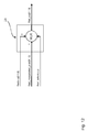
- FIG 2 showing schematically a first, a second and third pixel array 1, 2 and 3, each representing one of the chips of the 3-chip-CMOS camera.
- the first pixel array 1 is adapted to receive the red component
- the second pixel array 2 is adapted to receive the green component
- the third pixel array is adapted to receive the blue component from an incoming original image, which is split up in its RGB-components.
- the pixel at the position R(x,y) in the first pixel array is a defect pixel 4.
- each other pixel in each other pixel array could be used in an analogue manner.
- the pixels surrounding the defect pixel 4 in the same first pixel array 1 are named neighbouring pixels 5 and are referenced by the positions from R(x-1, y-1) to R(x+1, y+1).
- the pixels of the other two pixel arrays 2, 3 at the same location are named corresponding pixels 6, 7 and are referenced by the positions G(x,y) and B(x,y) respectively.
- the pixels surrounding the corresponding pixels 6,7 are named neighbouring pixels 8, 9, respectively, and are defined in an analogue manner as the neighbouring pixels 5.
- pixels of various pixel arrays are at the same location means that these pixels together form a RGB-image point of an output image.
- the first step 100 of the method is the calculation of directional interpolation values for the defect pixel 4 by evaluating the neighbouring pixels 5.
- the four main directions are evaluated, which are according to fig. 3 a vertical interpolation, according to fig. 4 a horizontal interpolation, according to fig. 5 a first diagonal interpolation and according to fig. 6 a second diagonal interpolation.
- Each directional interpolation is carried out by calculating the mean value of the values of two pixels of the neighbouring pixels 5, whereby the said two pixels lay on a line of the respective main direction and surround the defect pixel 5.
- the mean value of the pixels with the positions R(x,y-1) and R(x,y+1) is calculated as the directional interpolation value.
- a confidence value for each directional interpolation value is estimated by evaluating the values of the corresponding pixels 6, 7 and the neighbouring pixels 8, 9 of the second and third pixel array 2, 3.
- the confidence values concerning the other main directions are calculated in an analogue manner.
- a third step 300 the results of the directional interpolation operation are mixed in a weighted manner in dependence on the confidence values. This operation is also performed to avoid blinking pixels.
- the mixing operation is performed stepwise, whereby in a first step two directional interpolation values are mixed, respectively, and in a second step the resulting two intermediate values are mixed. As a result of the mixing operation a corrected pixel value is output.
- fig. 10 and fig. 11 For details of the mixing operation, reference is made to fig. 10 and fig. 11 .
- a fourth step 400 the defect pixel value is replaced by the corrected pixel value, so that the output image comprises instead of defect pixel values the estimated corrected pixel values thus improving significantly the quality of the output image.
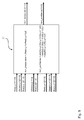
- Fig. 7 shows a first embodiment of a processing device 10 as a schematic block diagram.
- the processing device is for example realised in CMOS-technology and is part of the above-mentioned three-chip-camera.
- the processing device 10 comprises three input channels 11, 12, 13, whereby the first input channel 11 is adapted for receiving the red pixel values of the first pixel array 1, the second input channel 12 is adapted for receiving the green pixel values of the second pixel array 2 and the third input channel 13 is adapted for receiving the blue pixel values of the third pixel array 3.
- Each of the channels is divided in an information section, for example Red_in[11:0], for receiving 12-Bit pixel values and in an error section, for example Red_defect ,for receiving a 1-Bit value (this signal is equal to 1 when the corresponding pixel is defect, to 0 otherwise) for a defect pixel.
- an information section for example Red_in[11:0]
- an error section for example Red_defect ,for receiving a 1-Bit value (this signal is equal to 1 when the corresponding pixel is defect, to 0 otherwise) for a defect pixel.
- the input signals are sent to a pixel_distribution block 14, which is basically a memory.
- the pixel values are guided to one of the defect_pixel_correction blocks 15, 16, 17, whereby each block receives 26 pixel values for generating corrected pixel values.
- the red_defect_pixel_correction block 15 for example receives in the situation of figure 2 the 8 values of the neighbouring pixels 5, 8 and 9, respectively (i.e. 24 values) and the 2 values of the corresponding pixels 6 and 7 (i.e. 2 values).
- the defect pixel value(s), for example defect pixel 4 are replaced by the corrected pixel values and sent to output channels 18, 19 and 20 of the processing device 10, whereby the signals of the output channels 18, 19 and 20 show instead of defect pixels values the replaced corrected pixel values.
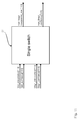
- Figure 8 shows the red_defect_pixel_correction block 15 in a more detailed schematic block diagram.
- the green_defect_pixel_correction block 16 and the blue_defect_pixel_correction block 17 are constructed in an analogue manner.
- the red_defect_pixel_correction block 15 is composed by four identical direction_interpolator blocks 21, 22, 23, 24, which generate interpolation values for the respective direction, and confidence values corresponding to the confidence to the interpolation values as explained in connection with figures 3 to 6 .
- a soft_switch 25 mixes the different interpolation values depending on the confidence values especially in order to avoid blinking pixels.
- a replacement_switch block 26 only switches between the input value and the corrected value depending on the red_defect(x,y) bit.
- Figure 9 illustrates the verticular_interpolator block 21 in a more detailed presentation also as a block diagram.
- the other interpolators 22, 23, 24 are - besides the inputs - identical or analogue, so that by means of example only the red_vertical_interpolator is described.
- the verticular_interpolator block 21 generates an interpolation value vert_interpolation [11:0], which is an average between two neighbour pixels (see also figure 3 ) in the interpolation direction.
- a vert_confidence [13:0] value is calculated by the formula as already explained above.
- some results can be shared by the different direction_interpolator blocks 21, 22, 23, 24: For example if the interpolation values of Red_vertical_interpolator, Green_vertical_interpolator and Blue_vertical_interpolator are calculated, these values can be used for the computation of Red_vertical_confidence. Also the value abs(G(x,y)-(G(x,y-1)+G(x,y+1))/2) can be used for the computation of Red_vertical_confidence and the computation of Blue_vertical_confidence.
- the soft_switch 25 in figure 10 merges or mixes the interpolated values from the interpolators 21, 22, 23, 24 in dependence on the confidence values.
- the mixing operation is done stepwise, whereby in a first step in a first single switch block 27 the interpolated values from the vertical interpolator 21 and from the diagonal 1_interpolator 22 are mixed. In a second single switch block 28 parallel to the first single switch block 27 the interpolated values from the horizontal_interpolator 21 and from the diagonal2_interpolator 22 are mixed.
- Each of the single switch_blocks 27 and 28 generates an intermediate interpolated value and an intermediate confidence value, which are guided into a third single switch block 29.
- the third single switch 29 mixes the intermediate interpolated into the corrected pixel value interpolated_pixel [11:0], which is then guided to the replacement switch block 26.
- the mixing operation in the single_switch blocks 27, 28 and 29 is explained by means of example for the first single_switch block 27 in connection with figure 11 .
- the first single_switch block 27 receives the value vert_interpolation [11:0] from the vertical interpolator 21, the respective confidence value vert_confidence [13:0], the value diag1_interpolation [11:0] from the diagonal1_interpolator 22 and the respective confidence value diag1_confidence [13:0] as input values. As output values, the first single_switch block generates an intermediate interpolated value vert_diag1_interpolated_pixel[11:0] and a respective confidence value vert_diag1_confidence[13:0].
- the intermediate interpolated value vert_diag1_interpolated_pixel is equal to the median value of:
- the intermediate interpolated value vert_diag1_interpolated_pixel lies between the two input values (vert_interpolation and diag1_interpolation). If the two confidence values are equal this intermediate interpolated value is equal to the average of these two input values, otherwise the intermediate interpolated value is closer (or equal) to the input value having the smaller confidence value.
- vert_diag1_confidence is equal to the minimum of the two confidence values. (The third single switch block 29 does not need this computation since this value will not be used).
Landscapes
- Engineering & Computer Science (AREA)
- Multimedia (AREA)
- Signal Processing (AREA)
- Color Television Image Signal Generators (AREA)
- Transforming Light Signals Into Electric Signals (AREA)
Priority Applications (5)
| Application Number | Priority Date | Filing Date | Title |
|---|---|---|---|
| EP07301218A EP2015562A1 (de) | 2007-07-10 | 2007-07-10 | Verarbeitungsvorrichtung zum Korrigieren fehlerhafter Pixelwerte eines Bildsensors, Bildsensor mit der Verarbeitungsvorrichtung sowie Verfahren |
| PCT/EP2008/057565 WO2009007199A1 (en) | 2007-07-10 | 2008-06-16 | Processing device for correcting defect pixel values of an image sensor unit, image sensor unit with the processing device and method |
| US12/452,556 US8502892B2 (en) | 2007-07-10 | 2008-06-16 | Processing device for correcting defect pixel values of an image sensor unit, image sensor unit with the processing device and method |
| EP20080761074 EP2163085A1 (de) | 2007-07-10 | 2008-06-16 | Verarbeitungseinrichtung zur korrektur defekter pixelwerte einer bildsensoreinheit, bildsensoreinheit mit der verarbeitungseinrichtung und verfahren |
| JP2010515450A JP5264902B2 (ja) | 2007-07-10 | 2008-06-16 | イメージセンサユニットの異常画素値を修正する処理装置、その処理装置を有するイメージセンサユニット及び方法 |
Applications Claiming Priority (1)
| Application Number | Priority Date | Filing Date | Title |
|---|---|---|---|
| EP07301218A EP2015562A1 (de) | 2007-07-10 | 2007-07-10 | Verarbeitungsvorrichtung zum Korrigieren fehlerhafter Pixelwerte eines Bildsensors, Bildsensor mit der Verarbeitungsvorrichtung sowie Verfahren |
Publications (1)
| Publication Number | Publication Date |
|---|---|
| EP2015562A1 true EP2015562A1 (de) | 2009-01-14 |
Family
ID=38668481
Family Applications (2)
| Application Number | Title | Priority Date | Filing Date |
|---|---|---|---|
| EP07301218A Withdrawn EP2015562A1 (de) | 2007-07-10 | 2007-07-10 | Verarbeitungsvorrichtung zum Korrigieren fehlerhafter Pixelwerte eines Bildsensors, Bildsensor mit der Verarbeitungsvorrichtung sowie Verfahren |
| EP20080761074 Ceased EP2163085A1 (de) | 2007-07-10 | 2008-06-16 | Verarbeitungseinrichtung zur korrektur defekter pixelwerte einer bildsensoreinheit, bildsensoreinheit mit der verarbeitungseinrichtung und verfahren |
Family Applications After (1)
| Application Number | Title | Priority Date | Filing Date |
|---|---|---|---|
| EP20080761074 Ceased EP2163085A1 (de) | 2007-07-10 | 2008-06-16 | Verarbeitungseinrichtung zur korrektur defekter pixelwerte einer bildsensoreinheit, bildsensoreinheit mit der verarbeitungseinrichtung und verfahren |
Country Status (4)
| Country | Link |
|---|---|
| US (1) | US8502892B2 (de) |
| EP (2) | EP2015562A1 (de) |
| JP (1) | JP5264902B2 (de) |
| WO (1) | WO2009007199A1 (de) |
Cited By (18)
| Publication number | Priority date | Publication date | Assignee | Title |
|---|---|---|---|---|
| WO2011049777A1 (en) * | 2009-10-20 | 2011-04-28 | Apple Inc. | System and method for detecting and correcting defective pixels in an image sensor |
| EP2450849A1 (de) * | 2010-11-05 | 2012-05-09 | Raytheon Company | Ungleichförmigkeitskorrekturverfahren basierend auf FIFO-gepufferte Szene |
| US20120113266A1 (en) * | 2009-04-07 | 2012-05-10 | Nextvision Stabilized Systems Ltd | Methods of manufacturing a camera system having multiple image sensors |
| US8817120B2 (en) | 2012-05-31 | 2014-08-26 | Apple Inc. | Systems and methods for collecting fixed pattern noise statistics of image data |
| US8872946B2 (en) | 2012-05-31 | 2014-10-28 | Apple Inc. | Systems and methods for raw image processing |
| US8917336B2 (en) | 2012-05-31 | 2014-12-23 | Apple Inc. | Image signal processing involving geometric distortion correction |
| US8953882B2 (en) | 2012-05-31 | 2015-02-10 | Apple Inc. | Systems and methods for determining noise statistics of image data |
| US9014504B2 (en) | 2012-05-31 | 2015-04-21 | Apple Inc. | Systems and methods for highlight recovery in an image signal processor |
| US9025867B2 (en) | 2012-05-31 | 2015-05-05 | Apple Inc. | Systems and methods for YCC image processing |
| US9031319B2 (en) | 2012-05-31 | 2015-05-12 | Apple Inc. | Systems and methods for luma sharpening |
| US9077943B2 (en) | 2012-05-31 | 2015-07-07 | Apple Inc. | Local image statistics collection |
| US9105078B2 (en) | 2012-05-31 | 2015-08-11 | Apple Inc. | Systems and methods for local tone mapping |
| US9131196B2 (en) | 2012-05-31 | 2015-09-08 | Apple Inc. | Systems and methods for defective pixel correction with neighboring pixels |
| US9142012B2 (en) | 2012-05-31 | 2015-09-22 | Apple Inc. | Systems and methods for chroma noise reduction |
| US9332239B2 (en) | 2012-05-31 | 2016-05-03 | Apple Inc. | Systems and methods for RGB image processing |
| CN110264489A (zh) * | 2019-06-24 | 2019-09-20 | 北京奇艺世纪科技有限公司 | 一种图像边界检测方法、装置及终端 |
| US11089247B2 (en) | 2012-05-31 | 2021-08-10 | Apple Inc. | Systems and method for reducing fixed pattern noise in image data |
| CN116504169A (zh) * | 2023-06-27 | 2023-07-28 | 联士光电(深圳)有限公司 | 显示设备 |
Families Citing this family (6)
| Publication number | Priority date | Publication date | Assignee | Title |
|---|---|---|---|---|
| US7974805B2 (en) * | 2008-10-14 | 2011-07-05 | ON Semiconductor Trading, Ltd | Image sensor and method |
| JP5458223B1 (ja) * | 2012-04-10 | 2014-04-02 | オリンパスメディカルシステムズ株式会社 | 撮像装置 |
| KR101407311B1 (ko) * | 2012-10-31 | 2014-06-13 | 엘지디스플레이 주식회사 | 터치표시장치 및 이의 광센서모듈 복구방법 |
| US9390663B2 (en) * | 2014-02-07 | 2016-07-12 | Nvidia Corporation | Liquid crystal display overdrive interpolation circuit and method |
| CN107305695B (zh) * | 2016-04-14 | 2021-03-09 | 上海富瀚微电子股份有限公司 | 一种图像自动坏点校正装置及方法 |
| JP2019205085A (ja) * | 2018-05-24 | 2019-11-28 | キヤノン株式会社 | 撮像装置、画像処理装置及び方法 |
Citations (6)
| Publication number | Priority date | Publication date | Assignee | Title |
|---|---|---|---|---|
| EP0440563A2 (de) * | 1990-01-31 | 1991-08-07 | Sony Corporation | Schaltung zur Bildfehlerkorrektur für eine FestkÀ¶rperbildaufnahmevorrichtung |
| EP0635973A1 (de) * | 1993-07-23 | 1995-01-25 | Koninklijke Philips Electronics N.V. | Signalkorrektur |
| EP1178676A1 (de) * | 2000-07-31 | 2002-02-06 | Hitachi Kokusai Electric Inc. | Verfahren und Vorrichtung zur Erkennung von defekten Bildelementen einer Halbleiterfarbbildaufnahmevorrichtung |
| US20040150731A1 (en) * | 2003-01-23 | 2004-08-05 | Sony Corporation | Pixel compensating circuit, method for compensating pixels, and image taking apparatus employing such pixel compensating circuit |
| EP1662771A2 (de) * | 2004-11-29 | 2006-05-31 | Sony Corporation | Datenverarbeitungsvorrichtung und -verfahren, Datenträger und Programm. |
| EP1679654A1 (de) * | 2005-01-11 | 2006-07-12 | STMicroelectronics (Research & Development) Limited | Verbesserte digitale Filterung |
Family Cites Families (6)
| Publication number | Priority date | Publication date | Assignee | Title |
|---|---|---|---|---|
| JPH06153087A (ja) * | 1992-09-17 | 1994-05-31 | Sony Corp | 画素欠陥補正方法 |
| JP3704238B2 (ja) * | 1997-03-31 | 2005-10-12 | 株式会社リコー | 撮像装置 |
| JP4115574B2 (ja) * | 1998-02-02 | 2008-07-09 | オリンパス株式会社 | 撮像装置 |
| US6794627B2 (en) * | 2001-10-24 | 2004-09-21 | Foveon, Inc. | Aggregation of active pixel sensor signals |
| WO2005096218A1 (en) * | 2004-03-31 | 2005-10-13 | Canon Kabushiki Kaisha | Imaging system performance measurement |
| JP5016255B2 (ja) * | 2006-02-22 | 2012-09-05 | 富士フイルム株式会社 | ノイズ低減装置ならびにその制御方法およびその制御プログラムならびに撮像装置およびディジタル・カメラ |
-
2007
- 2007-07-10 EP EP07301218A patent/EP2015562A1/de not_active Withdrawn
-
2008
- 2008-06-16 US US12/452,556 patent/US8502892B2/en not_active Expired - Fee Related
- 2008-06-16 EP EP20080761074 patent/EP2163085A1/de not_active Ceased
- 2008-06-16 JP JP2010515450A patent/JP5264902B2/ja not_active Expired - Fee Related
- 2008-06-16 WO PCT/EP2008/057565 patent/WO2009007199A1/en active Application Filing
Patent Citations (6)
| Publication number | Priority date | Publication date | Assignee | Title |
|---|---|---|---|---|
| EP0440563A2 (de) * | 1990-01-31 | 1991-08-07 | Sony Corporation | Schaltung zur Bildfehlerkorrektur für eine FestkÀ¶rperbildaufnahmevorrichtung |
| EP0635973A1 (de) * | 1993-07-23 | 1995-01-25 | Koninklijke Philips Electronics N.V. | Signalkorrektur |
| EP1178676A1 (de) * | 2000-07-31 | 2002-02-06 | Hitachi Kokusai Electric Inc. | Verfahren und Vorrichtung zur Erkennung von defekten Bildelementen einer Halbleiterfarbbildaufnahmevorrichtung |
| US20040150731A1 (en) * | 2003-01-23 | 2004-08-05 | Sony Corporation | Pixel compensating circuit, method for compensating pixels, and image taking apparatus employing such pixel compensating circuit |
| EP1662771A2 (de) * | 2004-11-29 | 2006-05-31 | Sony Corporation | Datenverarbeitungsvorrichtung und -verfahren, Datenträger und Programm. |
| EP1679654A1 (de) * | 2005-01-11 | 2006-07-12 | STMicroelectronics (Research & Development) Limited | Verbesserte digitale Filterung |
Cited By (30)
| Publication number | Priority date | Publication date | Assignee | Title |
|---|---|---|---|---|
| US20120113266A1 (en) * | 2009-04-07 | 2012-05-10 | Nextvision Stabilized Systems Ltd | Methods of manufacturing a camera system having multiple image sensors |
| WO2011049777A1 (en) * | 2009-10-20 | 2011-04-28 | Apple Inc. | System and method for detecting and correcting defective pixels in an image sensor |
| CN102640489A (zh) * | 2009-10-20 | 2012-08-15 | 苹果公司 | 用于检测和校正图像传感器中的缺陷像素的系统和方法 |
| US8259198B2 (en) | 2009-10-20 | 2012-09-04 | Apple Inc. | System and method for detecting and correcting defective pixels in an image sensor |
| TWI425831B (zh) * | 2009-10-20 | 2014-02-01 | Apple Inc | 偵測及校正影像感測器中之缺陷像素之系統及方法 |
| EP2450849A1 (de) * | 2010-11-05 | 2012-05-09 | Raytheon Company | Ungleichförmigkeitskorrekturverfahren basierend auf FIFO-gepufferte Szene |
| US8625005B2 (en) | 2010-11-05 | 2014-01-07 | Raytheon Company | First-in-first-out (FIFO) buffered median scene non-uniformity correction method |
| US9077943B2 (en) | 2012-05-31 | 2015-07-07 | Apple Inc. | Local image statistics collection |
| US9317930B2 (en) | 2012-05-31 | 2016-04-19 | Apple Inc. | Systems and methods for statistics collection using pixel mask |
| US8917336B2 (en) | 2012-05-31 | 2014-12-23 | Apple Inc. | Image signal processing involving geometric distortion correction |
| US8953882B2 (en) | 2012-05-31 | 2015-02-10 | Apple Inc. | Systems and methods for determining noise statistics of image data |
| US9014504B2 (en) | 2012-05-31 | 2015-04-21 | Apple Inc. | Systems and methods for highlight recovery in an image signal processor |
| US9025867B2 (en) | 2012-05-31 | 2015-05-05 | Apple Inc. | Systems and methods for YCC image processing |
| US9031319B2 (en) | 2012-05-31 | 2015-05-12 | Apple Inc. | Systems and methods for luma sharpening |
| US8817120B2 (en) | 2012-05-31 | 2014-08-26 | Apple Inc. | Systems and methods for collecting fixed pattern noise statistics of image data |
| US9105078B2 (en) | 2012-05-31 | 2015-08-11 | Apple Inc. | Systems and methods for local tone mapping |
| US9131196B2 (en) | 2012-05-31 | 2015-09-08 | Apple Inc. | Systems and methods for defective pixel correction with neighboring pixels |
| US9142012B2 (en) | 2012-05-31 | 2015-09-22 | Apple Inc. | Systems and methods for chroma noise reduction |
| US8872946B2 (en) | 2012-05-31 | 2014-10-28 | Apple Inc. | Systems and methods for raw image processing |
| US9332239B2 (en) | 2012-05-31 | 2016-05-03 | Apple Inc. | Systems and methods for RGB image processing |
| US9342858B2 (en) | 2012-05-31 | 2016-05-17 | Apple Inc. | Systems and methods for statistics collection using clipped pixel tracking |
| US9710896B2 (en) | 2012-05-31 | 2017-07-18 | Apple Inc. | Systems and methods for chroma noise reduction |
| US9743057B2 (en) | 2012-05-31 | 2017-08-22 | Apple Inc. | Systems and methods for lens shading correction |
| US9741099B2 (en) | 2012-05-31 | 2017-08-22 | Apple Inc. | Systems and methods for local tone mapping |
| US11689826B2 (en) | 2012-05-31 | 2023-06-27 | Apple Inc. | Systems and method for reducing fixed pattern noise in image data |
| US11089247B2 (en) | 2012-05-31 | 2021-08-10 | Apple Inc. | Systems and method for reducing fixed pattern noise in image data |
| CN110264489B (zh) * | 2019-06-24 | 2022-07-05 | 北京奇艺世纪科技有限公司 | 一种图像边界检测方法、装置及终端 |
| CN110264489A (zh) * | 2019-06-24 | 2019-09-20 | 北京奇艺世纪科技有限公司 | 一种图像边界检测方法、装置及终端 |
| CN116504169A (zh) * | 2023-06-27 | 2023-07-28 | 联士光电(深圳)有限公司 | 显示设备 |
| CN116504169B (zh) * | 2023-06-27 | 2023-09-08 | 联士光电(深圳)有限公司 | 显示设备 |
Also Published As
| Publication number | Publication date |
|---|---|
| US20100110240A1 (en) | 2010-05-06 |
| JP5264902B2 (ja) | 2013-08-14 |
| JP2010532960A (ja) | 2010-10-14 |
| EP2163085A1 (de) | 2010-03-17 |
| US8502892B2 (en) | 2013-08-06 |
| WO2009007199A1 (en) | 2009-01-15 |
Similar Documents
| Publication | Publication Date | Title |
|---|---|---|
| US8502892B2 (en) | Processing device for correcting defect pixel values of an image sensor unit, image sensor unit with the processing device and method | |
| JP4161295B2 (ja) | 画像センサのダイナミックレンジを拡大するカラー画像撮像システム | |
| US7015961B2 (en) | Digital image system and method for combining demosaicing and bad pixel correction | |
| RU2556022C2 (ru) | Устройство формирования цветного изображения | |
| US7602418B2 (en) | Digital image with reduced object motion blur | |
| JP3988457B2 (ja) | 撮像装置及び固体撮像素子の信号処理方法 | |
| US20100149393A1 (en) | Increasing the resolution of color sub-pixel arrays | |
| US7911514B2 (en) | Defective pixel correction device | |
| US8891899B2 (en) | Methods, systems and apparatuses for pixel value correction using multiple vertical and/or horizontal correction curves | |
| Catrysse et al. | Roadmap for CMOS image sensors: Moore meets Planck and Sommerfeld | |
| CN101262564A (zh) | 图像处理装置、成像装置、图像处理方法和计算机程序 | |
| JP2007174117A (ja) | 画像処理回路および画像処理方法 | |
| US6833868B1 (en) | Method and device for determining corrected color aspects of a pixel in an imaging device | |
| US6727945B1 (en) | Color signal interpolation | |
| US8970747B2 (en) | Imaging device | |
| US6441849B1 (en) | Image pickup system for obtaining an image signal at a proper level with high definition from an arbitrary small area selected from all image pickup areas | |
| CN103621070B (zh) | 摄像装置及摄像装置的控制方法 | |
| JP4934991B2 (ja) | 撮像信号処理装置及び方法並びに撮像装置 | |
| JP2004023683A (ja) | 固体撮像素子の欠陥補正装置及び方法 | |
| KR100733010B1 (ko) | 이미지 센서의 결함픽셀 보간 방법 및 장치 | |
| US7916188B2 (en) | Correction approximating straight line group information generating method of multi-divided reading CCD, and correction processing device manufacturing method of multi-divided reading CCD | |
| JP2001231052A (ja) | 固体撮像素子出力信号処理方法およびそれを用いたカメラ | |
| KR20070070674A (ko) | 색차 신호를 이용한 불량 화소 보간 장치 및 그 방법 | |
| JP2005086630A (ja) | 撮像装置 | |
| US6674465B1 (en) | Image processing apparatus which does not generate a false signal even if unevenness of spectral sensitivities of the color filter occurs |
Legal Events
| Date | Code | Title | Description |
|---|---|---|---|
| PUAI | Public reference made under article 153(3) epc to a published international application that has entered the european phase |
Free format text: ORIGINAL CODE: 0009012 |
|
| AK | Designated contracting states |
Kind code of ref document: A1 Designated state(s): AT BE BG CH CY CZ DE DK EE ES FI FR GB GR HU IE IS IT LI LT LU LV MC MT NL PL PT RO SE SI SK TR |
|
| AX | Request for extension of the european patent |
Extension state: AL BA HR MK RS |
|
| AKX | Designation fees paid | ||
| STAA | Information on the status of an ep patent application or granted ep patent |
Free format text: STATUS: THE APPLICATION IS DEEMED TO BE WITHDRAWN |
|
| 18D | Application deemed to be withdrawn |
Effective date: 20090715 |
|
| REG | Reference to a national code |
Ref country code: DE Ref legal event code: 8566 |
|
| RTI1 | Title (correction) |
Free format text: PROCESSING DEVICE FOR CORRECTING DEFECT PIXEL VALUES OF A COLOUR IMAGE SENSOR UNIT, COLOUR IMAGE SENSOR UNIT WITH THE PROCESSING DEVICE AND METHOD |