EP2014739B1 - Verfahren zur Herstellung einer Nachbildung eines anisotropisch topologisch strukturierten Polymer-Films oder Beschichtung - Google Patents
Verfahren zur Herstellung einer Nachbildung eines anisotropisch topologisch strukturierten Polymer-Films oder Beschichtung Download PDFInfo
- Publication number
- EP2014739B1 EP2014739B1 EP08105038.7A EP08105038A EP2014739B1 EP 2014739 B1 EP2014739 B1 EP 2014739B1 EP 08105038 A EP08105038 A EP 08105038A EP 2014739 B1 EP2014739 B1 EP 2014739B1
- Authority
- EP
- European Patent Office
- Prior art keywords
- coating
- cross
- anisotropic
- replica
- layers
- Prior art date
- Legal status (The legal status is an assumption and is not a legal conclusion. Google has not performed a legal analysis and makes no representation as to the accuracy of the status listed.)
- Expired - Lifetime
Links
- 238000000576 coating method Methods 0.000 title claims abstract description 63
- 239000011248 coating agent Substances 0.000 title claims abstract description 39
- 229920006254 polymer film Polymers 0.000 title claims abstract description 11
- 238000004519 manufacturing process Methods 0.000 title claims description 9
- 239000000463 material Substances 0.000 claims abstract description 48
- 230000003287 optical effect Effects 0.000 claims abstract description 25
- 239000000758 substrate Substances 0.000 claims abstract description 20
- 239000000203 mixture Substances 0.000 claims abstract description 16
- 239000002904 solvent Substances 0.000 claims abstract description 15
- 238000000034 method Methods 0.000 claims description 34
- 238000004132 cross linking Methods 0.000 claims description 11
- 239000007788 liquid Substances 0.000 claims description 11
- 239000002184 metal Substances 0.000 claims description 9
- 229910052751 metal Inorganic materials 0.000 claims description 9
- 229920000642 polymer Polymers 0.000 claims description 9
- 150000002739 metals Chemical class 0.000 claims description 4
- 229920001730 Moisture cure polyurethane Polymers 0.000 claims description 3
- 239000003989 dielectric material Substances 0.000 claims description 3
- 238000002156 mixing Methods 0.000 claims description 3
- 239000004094 surface-active agent Substances 0.000 claims description 3
- 239000002178 crystalline material Substances 0.000 claims description 2
- 239000011148 porous material Substances 0.000 abstract description 19
- 239000006117 anti-reflective coating Substances 0.000 abstract description 4
- 239000002086 nanomaterial Substances 0.000 abstract 2
- 239000010410 layer Substances 0.000 description 90
- 229920000106 Liquid crystal polymer Polymers 0.000 description 35
- 239000004977 Liquid-crystal polymers (LCPs) Substances 0.000 description 35
- 239000010408 film Substances 0.000 description 35
- 239000000178 monomer Substances 0.000 description 20
- XEKOWRVHYACXOJ-UHFFFAOYSA-N Ethyl acetate Chemical compound CCOC(C)=O XEKOWRVHYACXOJ-UHFFFAOYSA-N 0.000 description 15
- 239000004973 liquid crystal related substance Substances 0.000 description 15
- 239000011521 glass Substances 0.000 description 12
- 230000008569 process Effects 0.000 description 11
- 239000011243 crosslinked material Substances 0.000 description 10
- LFQSCWFLJHTTHZ-UHFFFAOYSA-N Ethanol Chemical compound CCO LFQSCWFLJHTTHZ-UHFFFAOYSA-N 0.000 description 8
- 239000000243 solution Substances 0.000 description 8
- 230000005540 biological transmission Effects 0.000 description 7
- 230000000694 effects Effects 0.000 description 7
- IJGRMHOSHXDMSA-UHFFFAOYSA-N Atomic nitrogen Chemical compound N#N IJGRMHOSHXDMSA-UHFFFAOYSA-N 0.000 description 6
- NLZUEZXRPGMBCV-UHFFFAOYSA-N Butylhydroxytoluene Chemical compound CC1=CC(C(C)(C)C)=C(O)C(C(C)(C)C)=C1 NLZUEZXRPGMBCV-UHFFFAOYSA-N 0.000 description 6
- 230000010287 polarization Effects 0.000 description 6
- 230000003667 anti-reflective effect Effects 0.000 description 5
- 101100203596 Caenorhabditis elegans sol-1 gene Proteins 0.000 description 4
- 230000015572 biosynthetic process Effects 0.000 description 4
- 230000000737 periodic effect Effects 0.000 description 4
- 101100184147 Caenorhabditis elegans mix-1 gene Proteins 0.000 description 3
- 238000004873 anchoring Methods 0.000 description 3
- 238000000089 atomic force micrograph Methods 0.000 description 3
- 230000008901 benefit Effects 0.000 description 3
- 230000008033 biological extinction Effects 0.000 description 3
- 238000009826 distribution Methods 0.000 description 3
- 238000005286 illumination Methods 0.000 description 3
- 239000003112 inhibitor Substances 0.000 description 3
- QSHDDOUJBYECFT-UHFFFAOYSA-N mercury Chemical compound [Hg] QSHDDOUJBYECFT-UHFFFAOYSA-N 0.000 description 3
- 229910052753 mercury Inorganic materials 0.000 description 3
- VLKZOEOYAKHREP-UHFFFAOYSA-N n-Hexane Chemical compound CCCCCC VLKZOEOYAKHREP-UHFFFAOYSA-N 0.000 description 3
- 229910052757 nitrogen Inorganic materials 0.000 description 3
- 239000004033 plastic Substances 0.000 description 3
- 229920003023 plastic Polymers 0.000 description 3
- 229920002959 polymer blend Polymers 0.000 description 3
- 238000002360 preparation method Methods 0.000 description 3
- 239000007787 solid Substances 0.000 description 3
- 238000003756 stirring Methods 0.000 description 3
- 239000000126 substance Substances 0.000 description 3
- 238000012546 transfer Methods 0.000 description 3
- 239000004988 Nematic liquid crystal Substances 0.000 description 2
- 239000004983 Polymer Dispersed Liquid Crystal Substances 0.000 description 2
- 239000004793 Polystyrene Substances 0.000 description 2
- WYURNTSHIVDZCO-UHFFFAOYSA-N Tetrahydrofuran Chemical compound C1CCOC1 WYURNTSHIVDZCO-UHFFFAOYSA-N 0.000 description 2
- 230000001680 brushing effect Effects 0.000 description 2
- 239000003086 colorant Substances 0.000 description 2
- BGTOWKSIORTVQH-UHFFFAOYSA-N cyclopentanone Chemical compound O=C1CCCC1 BGTOWKSIORTVQH-UHFFFAOYSA-N 0.000 description 2
- 230000001419 dependent effect Effects 0.000 description 2
- 239000000975 dye Substances 0.000 description 2
- 238000005259 measurement Methods 0.000 description 2
- 239000012528 membrane Substances 0.000 description 2
- 239000012788 optical film Substances 0.000 description 2
- 239000000123 paper Substances 0.000 description 2
- 238000000059 patterning Methods 0.000 description 2
- 229920003229 poly(methyl methacrylate) Polymers 0.000 description 2
- 239000004926 polymethyl methacrylate Substances 0.000 description 2
- 238000011160 research Methods 0.000 description 2
- 230000003595 spectral effect Effects 0.000 description 2
- ZBTCSYDLYVZCDB-UHFFFAOYSA-N C=CC(OCCCCCCOc(cc1)ccc1C(Oc(cc1Cl)ccc1OC(c(cc1)ccc1OCCCCCCOC(C=C)=O)=O)=O)=O Chemical compound C=CC(OCCCCCCOc(cc1)ccc1C(Oc(cc1Cl)ccc1OC(c(cc1)ccc1OCCCCCCOC(C=C)=O)=O)=O)=O ZBTCSYDLYVZCDB-UHFFFAOYSA-N 0.000 description 1
- XDTMQSROBMDMFD-UHFFFAOYSA-N Cyclohexane Chemical compound C1CCCCC1 XDTMQSROBMDMFD-UHFFFAOYSA-N 0.000 description 1
- 241000282596 Hylobatidae Species 0.000 description 1
- 239000004904 UV filter Substances 0.000 description 1
- 238000010521 absorption reaction Methods 0.000 description 1
- 239000000654 additive Substances 0.000 description 1
- 230000000996 additive effect Effects 0.000 description 1
- 239000004411 aluminium Substances 0.000 description 1
- 229910052782 aluminium Inorganic materials 0.000 description 1
- XAGFODPZIPBFFR-UHFFFAOYSA-N aluminium Chemical compound [Al] XAGFODPZIPBFFR-UHFFFAOYSA-N 0.000 description 1
- 238000013459 approach Methods 0.000 description 1
- 238000004630 atomic force microscopy Methods 0.000 description 1
- 239000000987 azo dye Substances 0.000 description 1
- 210000004027 cell Anatomy 0.000 description 1
- 210000002421 cell wall Anatomy 0.000 description 1
- 230000002860 competitive effect Effects 0.000 description 1
- 150000001875 compounds Chemical class 0.000 description 1
- 238000010276 construction Methods 0.000 description 1
- 210000002858 crystal cell Anatomy 0.000 description 1
- 230000003247 decreasing effect Effects 0.000 description 1
- 238000005137 deposition process Methods 0.000 description 1
- 230000001066 destructive effect Effects 0.000 description 1
- 125000004386 diacrylate group Chemical group 0.000 description 1
- 238000004090 dissolution Methods 0.000 description 1
- 239000000428 dust Substances 0.000 description 1
- 230000005489 elastic deformation Effects 0.000 description 1
- 238000010894 electron beam technology Methods 0.000 description 1
- 238000000572 ellipsometry Methods 0.000 description 1
- 238000005530 etching Methods 0.000 description 1
- 125000004494 ethyl ester group Chemical group 0.000 description 1
- 238000001704 evaporation Methods 0.000 description 1
- 230000008020 evaporation Effects 0.000 description 1
- 230000004313 glare Effects 0.000 description 1
- 238000010438 heat treatment Methods 0.000 description 1
- 230000006872 improvement Effects 0.000 description 1
- 230000003993 interaction Effects 0.000 description 1
- 238000010884 ion-beam technique Methods 0.000 description 1
- 239000011159 matrix material Substances 0.000 description 1
- 239000011859 microparticle Substances 0.000 description 1
- 239000011259 mixed solution Substances 0.000 description 1
- 230000004048 modification Effects 0.000 description 1
- 238000012986 modification Methods 0.000 description 1
- 238000000465 moulding Methods 0.000 description 1
- 238000000399 optical microscopy Methods 0.000 description 1
- 239000002245 particle Substances 0.000 description 1
- 238000005191 phase separation Methods 0.000 description 1
- 238000005498 polishing Methods 0.000 description 1
- 229920002223 polystyrene Polymers 0.000 description 1
- 229920005553 polystyrene-acrylate Polymers 0.000 description 1
- 239000002243 precursor Substances 0.000 description 1
- 230000009467 reduction Effects 0.000 description 1
- 239000004065 semiconductor Substances 0.000 description 1
- 238000000926 separation method Methods 0.000 description 1
- 238000007493 shaping process Methods 0.000 description 1
- 239000002356 single layer Substances 0.000 description 1
- 238000003980 solgel method Methods 0.000 description 1
- 238000004528 spin coating Methods 0.000 description 1
- 230000003068 static effect Effects 0.000 description 1
- YLQBMQCUIZJEEH-UHFFFAOYSA-N tetrahydrofuran Natural products C=1C=COC=1 YLQBMQCUIZJEEH-UHFFFAOYSA-N 0.000 description 1
- 229920001169 thermoplastic Polymers 0.000 description 1
- 239000004416 thermosoftening plastic Substances 0.000 description 1
- 238000012876 topography Methods 0.000 description 1
Images
Classifications
-
- B—PERFORMING OPERATIONS; TRANSPORTING
- B05—SPRAYING OR ATOMISING IN GENERAL; APPLYING FLUENT MATERIALS TO SURFACES, IN GENERAL
- B05D—PROCESSES FOR APPLYING FLUENT MATERIALS TO SURFACES, IN GENERAL
- B05D5/00—Processes for applying liquids or other fluent materials to surfaces to obtain special surface effects, finishes or structures
- B05D5/06—Processes for applying liquids or other fluent materials to surfaces to obtain special surface effects, finishes or structures to obtain multicolour or other optical effects
- B05D5/061—Special surface effect
-
- C—CHEMISTRY; METALLURGY
- C09—DYES; PAINTS; POLISHES; NATURAL RESINS; ADHESIVES; COMPOSITIONS NOT OTHERWISE PROVIDED FOR; APPLICATIONS OF MATERIALS NOT OTHERWISE PROVIDED FOR
- C09K—MATERIALS FOR MISCELLANEOUS APPLICATIONS, NOT PROVIDED FOR ELSEWHERE
- C09K19/00—Liquid crystal materials
- C09K19/04—Liquid crystal materials characterised by the chemical structure of the liquid crystal components, e.g. by a specific unit
- C09K19/38—Polymers
-
- B—PERFORMING OPERATIONS; TRANSPORTING
- B29—WORKING OF PLASTICS; WORKING OF SUBSTANCES IN A PLASTIC STATE IN GENERAL
- B29C—SHAPING OR JOINING OF PLASTICS; SHAPING OF MATERIAL IN A PLASTIC STATE, NOT OTHERWISE PROVIDED FOR; AFTER-TREATMENT OF THE SHAPED PRODUCTS, e.g. REPAIRING
- B29C41/00—Shaping by coating a mould, core or other substrate, i.e. by depositing material and stripping-off the shaped article; Apparatus therefor
- B29C41/003—Shaping by coating a mould, core or other substrate, i.e. by depositing material and stripping-off the shaped article; Apparatus therefor characterised by the choice of material
-
- B—PERFORMING OPERATIONS; TRANSPORTING
- B82—NANOTECHNOLOGY
- B82Y—SPECIFIC USES OR APPLICATIONS OF NANOSTRUCTURES; MEASUREMENT OR ANALYSIS OF NANOSTRUCTURES; MANUFACTURE OR TREATMENT OF NANOSTRUCTURES
- B82Y30/00—Nanotechnology for materials or surface science, e.g. nanocomposites
-
- C—CHEMISTRY; METALLURGY
- C09—DYES; PAINTS; POLISHES; NATURAL RESINS; ADHESIVES; COMPOSITIONS NOT OTHERWISE PROVIDED FOR; APPLICATIONS OF MATERIALS NOT OTHERWISE PROVIDED FOR
- C09K—MATERIALS FOR MISCELLANEOUS APPLICATIONS, NOT PROVIDED FOR ELSEWHERE
- C09K19/00—Liquid crystal materials
- C09K19/52—Liquid crystal materials characterised by components which are not liquid crystals, e.g. additives with special physical aspect: solvents, solid particles
- C09K19/54—Additives having no specific mesophase characterised by their chemical composition
- C09K19/542—Macromolecular compounds
-
- C—CHEMISTRY; METALLURGY
- C09—DYES; PAINTS; POLISHES; NATURAL RESINS; ADHESIVES; COMPOSITIONS NOT OTHERWISE PROVIDED FOR; APPLICATIONS OF MATERIALS NOT OTHERWISE PROVIDED FOR
- C09K—MATERIALS FOR MISCELLANEOUS APPLICATIONS, NOT PROVIDED FOR ELSEWHERE
- C09K19/00—Liquid crystal materials
- C09K19/52—Liquid crystal materials characterised by components which are not liquid crystals, e.g. additives with special physical aspect: solvents, solid particles
- C09K19/54—Additives having no specific mesophase characterised by their chemical composition
- C09K19/56—Aligning agents
-
- G—PHYSICS
- G02—OPTICS
- G02B—OPTICAL ELEMENTS, SYSTEMS OR APPARATUS
- G02B1/00—Optical elements characterised by the material of which they are made; Optical coatings for optical elements
- G02B1/08—Optical elements characterised by the material of which they are made; Optical coatings for optical elements made of polarising materials
-
- G—PHYSICS
- G02—OPTICS
- G02B—OPTICAL ELEMENTS, SYSTEMS OR APPARATUS
- G02B1/00—Optical elements characterised by the material of which they are made; Optical coatings for optical elements
- G02B1/10—Optical coatings produced by application to, or surface treatment of, optical elements
- G02B1/11—Anti-reflection coatings
-
- G—PHYSICS
- G02—OPTICS
- G02B—OPTICAL ELEMENTS, SYSTEMS OR APPARATUS
- G02B5/00—Optical elements other than lenses
- G02B5/02—Diffusing elements; Afocal elements
- G02B5/0205—Diffusing elements; Afocal elements characterised by the diffusing properties
- G02B5/0257—Diffusing elements; Afocal elements characterised by the diffusing properties creating an anisotropic diffusion characteristic, i.e. distributing output differently in two perpendicular axes
-
- G—PHYSICS
- G02—OPTICS
- G02B—OPTICAL ELEMENTS, SYSTEMS OR APPARATUS
- G02B5/00—Optical elements other than lenses
- G02B5/18—Diffraction gratings
- G02B5/1847—Manufacturing methods
-
- G—PHYSICS
- G02—OPTICS
- G02B—OPTICAL ELEMENTS, SYSTEMS OR APPARATUS
- G02B5/00—Optical elements other than lenses
- G02B5/30—Polarising elements
- G02B5/3083—Birefringent or phase retarding elements
-
- G—PHYSICS
- G02—OPTICS
- G02F—OPTICAL DEVICES OR ARRANGEMENTS FOR THE CONTROL OF LIGHT BY MODIFICATION OF THE OPTICAL PROPERTIES OF THE MEDIA OF THE ELEMENTS INVOLVED THEREIN; NON-LINEAR OPTICS; FREQUENCY-CHANGING OF LIGHT; OPTICAL LOGIC ELEMENTS; OPTICAL ANALOGUE/DIGITAL CONVERTERS
- G02F1/00—Devices or arrangements for the control of the intensity, colour, phase, polarisation or direction of light arriving from an independent light source, e.g. switching, gating or modulating; Non-linear optics
- G02F1/01—Devices or arrangements for the control of the intensity, colour, phase, polarisation or direction of light arriving from an independent light source, e.g. switching, gating or modulating; Non-linear optics for the control of the intensity, phase, polarisation or colour
- G02F1/13—Devices or arrangements for the control of the intensity, colour, phase, polarisation or direction of light arriving from an independent light source, e.g. switching, gating or modulating; Non-linear optics for the control of the intensity, phase, polarisation or colour based on liquid crystals, e.g. single liquid crystal display cells
- G02F1/133—Constructional arrangements; Operation of liquid crystal cells; Circuit arrangements
- G02F1/1333—Constructional arrangements; Manufacturing methods
- G02F1/1337—Surface-induced orientation of the liquid crystal molecules, e.g. by alignment layers
- G02F1/133711—Surface-induced orientation of the liquid crystal molecules, e.g. by alignment layers by organic films, e.g. polymeric films
-
- G—PHYSICS
- G02—OPTICS
- G02F—OPTICAL DEVICES OR ARRANGEMENTS FOR THE CONTROL OF LIGHT BY MODIFICATION OF THE OPTICAL PROPERTIES OF THE MEDIA OF THE ELEMENTS INVOLVED THEREIN; NON-LINEAR OPTICS; FREQUENCY-CHANGING OF LIGHT; OPTICAL LOGIC ELEMENTS; OPTICAL ANALOGUE/DIGITAL CONVERTERS
- G02F1/00—Devices or arrangements for the control of the intensity, colour, phase, polarisation or direction of light arriving from an independent light source, e.g. switching, gating or modulating; Non-linear optics
- G02F1/01—Devices or arrangements for the control of the intensity, colour, phase, polarisation or direction of light arriving from an independent light source, e.g. switching, gating or modulating; Non-linear optics for the control of the intensity, phase, polarisation or colour
- G02F1/13—Devices or arrangements for the control of the intensity, colour, phase, polarisation or direction of light arriving from an independent light source, e.g. switching, gating or modulating; Non-linear optics for the control of the intensity, phase, polarisation or colour based on liquid crystals, e.g. single liquid crystal display cells
- G02F1/133—Constructional arrangements; Operation of liquid crystal cells; Circuit arrangements
- G02F1/1333—Constructional arrangements; Manufacturing methods
- G02F1/1337—Surface-induced orientation of the liquid crystal molecules, e.g. by alignment layers
- G02F1/13378—Surface-induced orientation of the liquid crystal molecules, e.g. by alignment layers by treatment of the surface, e.g. embossing, rubbing or light irradiation
-
- B—PERFORMING OPERATIONS; TRANSPORTING
- B29—WORKING OF PLASTICS; WORKING OF SUBSTANCES IN A PLASTIC STATE IN GENERAL
- B29K—INDEXING SCHEME ASSOCIATED WITH SUBCLASSES B29B, B29C OR B29D, RELATING TO MOULDING MATERIALS OR TO MATERIALS FOR MOULDS, REINFORCEMENTS, FILLERS OR PREFORMED PARTS, e.g. INSERTS
- B29K2995/00—Properties of moulding materials, reinforcements, fillers, preformed parts or moulds
- B29K2995/0037—Other properties
- B29K2995/0072—Roughness, e.g. anti-slip
-
- C—CHEMISTRY; METALLURGY
- C09—DYES; PAINTS; POLISHES; NATURAL RESINS; ADHESIVES; COMPOSITIONS NOT OTHERWISE PROVIDED FOR; APPLICATIONS OF MATERIALS NOT OTHERWISE PROVIDED FOR
- C09K—MATERIALS FOR MISCELLANEOUS APPLICATIONS, NOT PROVIDED FOR ELSEWHERE
- C09K2323/00—Functional layers of liquid crystal optical display excluding electroactive liquid crystal layer characterised by chemical composition
- C09K2323/02—Alignment layer characterised by chemical composition
-
- G—PHYSICS
- G02—OPTICS
- G02F—OPTICAL DEVICES OR ARRANGEMENTS FOR THE CONTROL OF LIGHT BY MODIFICATION OF THE OPTICAL PROPERTIES OF THE MEDIA OF THE ELEMENTS INVOLVED THEREIN; NON-LINEAR OPTICS; FREQUENCY-CHANGING OF LIGHT; OPTICAL LOGIC ELEMENTS; OPTICAL ANALOGUE/DIGITAL CONVERTERS
- G02F1/00—Devices or arrangements for the control of the intensity, colour, phase, polarisation or direction of light arriving from an independent light source, e.g. switching, gating or modulating; Non-linear optics
- G02F1/01—Devices or arrangements for the control of the intensity, colour, phase, polarisation or direction of light arriving from an independent light source, e.g. switching, gating or modulating; Non-linear optics for the control of the intensity, phase, polarisation or colour
- G02F1/13—Devices or arrangements for the control of the intensity, colour, phase, polarisation or direction of light arriving from an independent light source, e.g. switching, gating or modulating; Non-linear optics for the control of the intensity, phase, polarisation or colour based on liquid crystals, e.g. single liquid crystal display cells
- G02F1/137—Devices or arrangements for the control of the intensity, colour, phase, polarisation or direction of light arriving from an independent light source, e.g. switching, gating or modulating; Non-linear optics for the control of the intensity, phase, polarisation or colour based on liquid crystals, e.g. single liquid crystal display cells characterised by the electro-optical or magneto-optical effect, e.g. field-induced phase transition, orientation effect, guest-host interaction or dynamic scattering
- G02F1/139—Devices or arrangements for the control of the intensity, colour, phase, polarisation or direction of light arriving from an independent light source, e.g. switching, gating or modulating; Non-linear optics for the control of the intensity, phase, polarisation or colour based on liquid crystals, e.g. single liquid crystal display cells characterised by the electro-optical or magneto-optical effect, e.g. field-induced phase transition, orientation effect, guest-host interaction or dynamic scattering based on orientation effects in which the liquid crystal remains transparent
- G02F1/1391—Bistable or multi-stable liquid crystal cells
-
- Y—GENERAL TAGGING OF NEW TECHNOLOGICAL DEVELOPMENTS; GENERAL TAGGING OF CROSS-SECTIONAL TECHNOLOGIES SPANNING OVER SEVERAL SECTIONS OF THE IPC; TECHNICAL SUBJECTS COVERED BY FORMER USPC CROSS-REFERENCE ART COLLECTIONS [XRACs] AND DIGESTS
- Y10—TECHNICAL SUBJECTS COVERED BY FORMER USPC
- Y10T—TECHNICAL SUBJECTS COVERED BY FORMER US CLASSIFICATION
- Y10T428/00—Stock material or miscellaneous articles
- Y10T428/24—Structurally defined web or sheet [e.g., overall dimension, etc.]
- Y10T428/24479—Structurally defined web or sheet [e.g., overall dimension, etc.] including variation in thickness
- Y10T428/24521—Structurally defined web or sheet [e.g., overall dimension, etc.] including variation in thickness with component conforming to contour of nonplanar surface
-
- Y—GENERAL TAGGING OF NEW TECHNOLOGICAL DEVELOPMENTS; GENERAL TAGGING OF CROSS-SECTIONAL TECHNOLOGIES SPANNING OVER SEVERAL SECTIONS OF THE IPC; TECHNICAL SUBJECTS COVERED BY FORMER USPC CROSS-REFERENCE ART COLLECTIONS [XRACs] AND DIGESTS
- Y10—TECHNICAL SUBJECTS COVERED BY FORMER USPC
- Y10T—TECHNICAL SUBJECTS COVERED BY FORMER US CLASSIFICATION
- Y10T428/00—Stock material or miscellaneous articles
- Y10T428/24—Structurally defined web or sheet [e.g., overall dimension, etc.]
- Y10T428/24479—Structurally defined web or sheet [e.g., overall dimension, etc.] including variation in thickness
- Y10T428/2457—Parallel ribs and/or grooves
-
- Y—GENERAL TAGGING OF NEW TECHNOLOGICAL DEVELOPMENTS; GENERAL TAGGING OF CROSS-SECTIONAL TECHNOLOGIES SPANNING OVER SEVERAL SECTIONS OF THE IPC; TECHNICAL SUBJECTS COVERED BY FORMER USPC CROSS-REFERENCE ART COLLECTIONS [XRACs] AND DIGESTS
- Y10—TECHNICAL SUBJECTS COVERED BY FORMER USPC
- Y10T—TECHNICAL SUBJECTS COVERED BY FORMER US CLASSIFICATION
- Y10T428/00—Stock material or miscellaneous articles
- Y10T428/24—Structurally defined web or sheet [e.g., overall dimension, etc.]
- Y10T428/24942—Structurally defined web or sheet [e.g., overall dimension, etc.] including components having same physical characteristic in differing degree
Definitions
- This invention relates to a method of making a replica of an anisotropic topologically structured polymer film or coating.
- These films or coatings may find application as optical films or coatings and more particularly as orientation layers, optical retardation layers, anti-reflective coatings, and optical diffusers.
- the coatings typically exhibit sub-micron profiles such as pores, grooves, channels or stripes.
- a known isotropic topologically structured polymer coating is taught by Walheim et al in Science 283 (22 January 1999) 520-2 .
- a binary polymer blend (of polystyrene and polymethylmethacrylate dissolved in tetrahydrofuran) is allowed to demix to a controlled extent during spin coating onto a smooth substrate.
- cyclohexane which selectively dissolves polystyrene
- a porous coating of PMMA is obtained.
- This coating can be modified by varying the materials and the demixing times, but no long-range order or patterning of the topological structure can be imposed on it.
- WO 98/39673 discloses different methods for generating an anti-reflection coating.
- the coating has a rough surface with stochastically distributed structures, which are further modulated by periodically sequenced structures.
- the structures may be generated by photolithographic methods.
- the obtained surface structure is then transferred to a metal master, for example by a galvanic copy moulding process.
- the metal master or copies of the metal master are used as stamping dies for subsequent stamping processes, in which the surface structures are transferred to carrier layers, for instance by thermoplastic shaping or by UV hardening.
- EP 0216622 discloses a method for the production of microporous membranes, which comprises mixing a precursor material into a liquid vehicle, forming the composition into a thin liquid layer, exposing the liquid layer to ultraviolet or electron beam irradiation to cure the liquid layer and removing the liquid vehicle from the membrane.
- Such films or coatings could then be used, for example, as orientation layers (in some cases as bistable orientation layers) for liquid crystals and liquid crystal displays.
- Other technical applications become also feasible such as the production of low effective refractive index layers usable as antireflective coatings, or of optically diffusive layers, and the production of optically anisotropic coatings (especially of liquid crystal polymers) leading to novel optical components.
- photo-alignment photo-patterned grooved coatings are possible.
- substrates such as glass, plastics, metals, semiconductors or paper.
- the cross-linking is preferably effected by exposure to light such as UV light, which may be polarized, and contributes to a good stability of the film or coating.
- the cross-linkable material comprises molecules of a rod-like (calamitic) shape.
- the cross-linkable material and the non-cross-linkable material have chemical structures that are similar, i.e. with a good compatibility regarding miscibility.
- the cross-linkable material is liquid crystalline, and in such a case the non-cross-linkable material is also preferably mesogenic (liquid crystalline).
- a homogeneous transparent film may be formed and exposed to light, preferably UV light.
- the crosslinkable material is progressively being crosslinked, and the crosslinked material and the non-crosslinkable material demix gradually.
- the non-crosslinked material is removed with a selective solvent (or evaporated upon heating the layers) to create pores.
- a selective solvent or evaporated upon heating the layers
- the non-cross-linkable material may contain a surfactant.
- the crosslinkable material may contain an additive such as a dichroic dye.
- the cross-linkable material may be maintained in an oriented state during crosslinking, the orientation being imposed for example by an underlying orientation layer, which may be a photo-oriented layer such as an azo dye or linearly polymerized photopolymer, such being cheaper, simpler and much more versatile than a mechanically produced orientation layer.
- topological structures is based on the control of the demixing (nanophase separation) of two molecularly mixed components forming a homogeneous phase during crosslinking.
- a decisive advantage of this process is that size, shape and distribution of the topological structures can be adjusted over a wide range by a suitable choice of the experimental parameters, which are in particular the kind of solvent(s), the ratio of the mixture, the concentration in the solvent, and intensity and duration, wavelength, angle of incidence and state of polarization of light.
- crosslinking and the non-crosslinking materials are similar, and especially if a surfactant is added, a molecularly well mixed solution can be achieved, which additionally ensures that the crosslinking process is the main cause of demixing.
- a further possibility to enhance the film homogeneity and the formation of nano-pores is the use, instead of one, of at least two solvents (Sol1 and Sol2) when preparing the mixture, whereby for instance Sol2 is a good solvent for the non-crosslinkable material and a poor solvent for the cross-linked material, e.g. hexane or ethanol, and Sol1 is a good solvent for the cross-linked material (may be a good or poor solvent for the non-cross-linkable material), e.g. ethylester.
- Sol1 and Sol2 are preferably selected to be miscible with each other.
- the present invention provides a method to fabricate a modulated (almost periodic) topology.
- the mixture preferably comprising a liquid crystalline material
- the orientation would induce elongation of the pores and lead to the formation of grooves (or channels, stripes, etc).
- Size and distribution of the "grooves" can be varied from a few nm to few ⁇ m depending on the preparation parameters (such as mixture, light irradiation time, temperature ).
- any method to orient the mixture can be used, such as employing a layer that induces an alignment of adjacent liquid crystal material.
- orientation layers made by photo-orientation methods (usually using linearly polarized light), and especially well suited are linearly photo-polymerized (LPP) orientation layers, also known as photo-oriented polymer networks (PPN), among other things because these layers can be easily applied also to non-planar surfaces.
- LPP linearly photo-polymerized
- PPN photo-oriented polymer networks
- Such methods are for instance disclosed in US Patents 4974941 Gibbons et al , 5838407 Chigrinov et al , and 5602661 Schadt et al.
- An other possibility would be to use a mixture that itself contains a photo-orientable component. Examples of this kind of orientation method can for instance be found in the International Application PCT/IB99/01001 (ROLIC) filed 3 June 1999 .
- the first layer according to the invention has an aligned topological structure which is preferably aligned not parallel to the orientation of the cross-linked material (although parallel is possible for increased anchoring), the orientation and the alignment preferably being at right angles to each other.
- the alignment and crosslinking of the second layer may be induced by linearly polarized UV light.
- the UV light illumination can be adjusted such that the anchoring forces from the alignment and from the orientation are competitive with each other.
- the two materials may be dissolved in respective solvents before mixing, the solvents being mutually miscible but each being a poor solvent for the other solute.
- the cross-linkable material may be present in a proportion of 1/10 to 30 parts, preferably 1/4 to 4 parts, by weight per part of non-cross-linkable material, the latter being destined for dissolution out of the finished coating.
- the structure may comprise hollows at least 99% of which are smaller than 1000 nm, preferably smaller than 500 nm, and more preferably smaller than 200 nm in at least one direction parallel to the coating plane. It will be understood that the hollows may arise from dissolving out the non-cross-linked material from the coating. The average distance between adjacent hollows is typically less than 500 nm, and the hollows may be elongated, which may be understood to be a result of orientation in the cross-linked material. In most applications, the coating, and in many also the substrate, are optically transparent.
- the substrate already has an aligned structure, achieved for example by employing a layer that induces an alignment of adjacent liquid crystal material.
- a layer that induces an alignment of adjacent liquid crystal material Particularly suitable are orientation layers made by photo-orientation methods (usually using linearly polarized light), and especially well suited are linearly photo-polymerized (LPP) orientation layers.
- LPP linearly photo-polymerized
- the aligned structure could alternatively be achieved by rubbing, brushing or other mechanical means.
- the said coating is applied thereto with an orientation which may be at from 0° to 90° to that alignment, or wherein this angle is different in different parts of the coating, optionally pixelwise.
- a topologically structured polymer film or coating can act as an optical diffuser.
- the holes or grooves as a rule have dimensions in the order of the wavelength of light.
- an antireflectively coated object comprising a coating or component as set forth above and to a liquid crystal cell wherein the liquid crystal molecules can adopt one of at least two different stable alignments in contact with a wall of the cell, the cell wall comprising a coating or component as set forth above.
- optical display device preferably a liquid crystal display, comprising a film or coating as set forth above.
- elements are used for protection against forgery and copying.
- Antireflective coatings for the visible spectral region are required whenever light reflection of a surface is to be reduced or avoided.
- An example is the undesirable reflection of the glass of a display device.
- the basic principle of such coatings can be understood in terms of destructive interference between light reflected from air-film and film-substrate interfaces.
- Glass or plastic substrates for example, require a coating film with a low effective refractive index n eff ⁇ 1.2.
- n eff ⁇ 1.2 effective refractive index
- porous films can be used to reduce reflections at optical wavelengths.
- moth-eye the so-called "moth-eye" effect.
- the layer will appear as a continuous film with an effective refractive index given by an average over the film. Therefore, the challenge is to maximize the volume fraction of the pores in order to obtain very low n eff . It is the grading of the apparent refractive index that gives rise to the reduction in the reflection coefficient.
- Nano-porous crosslinked films can be produced using a simple process applicable to planar and especially also to non-planar surfaces. This process is based on the control of the phase separation of molecularly mixed compounds on the nanometre length scale. Depending on the preparation parameters, size, shape and volume fraction of pores can be accommodated. Using ellipsometric measurements we found that the effective refractive index (n eff ) of such layers can also be adjusted and decreased down to 1.2 or lower. Therefore the reflection coefficient off glasses can be efficiently reduced.
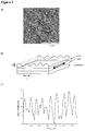
- a further advantage is the usually from top to bottom continuously narrowing shape of the pores/hollows (cf Figure 3c described in more detail later), because such "gradient hollows" have the effect that the refractive index changes continuously over the depth of the hollows, which in turn makes effective antireflection possible over a broad spectral region with only one layer.
- the elongated structure also affects the effective refractive index and makes it direction-dependent.
- Such layers can therefore also be used as antireflection layers that are sensitive to the angle of incidence.
- Orientation layers It is known that grooved surfaces can produce uniform and parallel alignment of liquid crystals due to anisotropic surface interactions. It is believed that this is because the periodic topology of mechanically grooved substrates minimises the elastic deformation energy of the liquid crystals by forcing the director to align along the grooves. Grooves are traditionally produced by rubbing (glasses plates, polymer layers, ...), unidirectional polishing, tangential evaporation, tangential ion-beam etching of oxides, or formation of a grating on the substrate. Although mechanical alignment is relatively simple, the techniques used to produce the grooves are, however, difficult to implement, involve expensive equipment, and are relatively slow.
- brushing (rubbing) processes have several inherent disadvantages such as the generation of dust particles and static surface charges.
- Another limitation is that mechanical alignment is a large-scale process and therefore not adapted to generate local variations (patterns) of the surface director, certainly not on the pixel scale.
- Films or coatings of crosslinked layers oriented as described above, show oriented grooves and therefore may be used as orientation layers for an adjacent liquid crystal material. It is believed that the alignment effect on liquid crystals is caused by the topology of the crosslinked layer, quite similar in effect to a brushed orientation layer.
- Optical retarders It is known that for a layer with modulated surface profile, such as linear gratings or porous films with an inclined columnar structure formed in vapour deposition processes at an oblique angle, the apparent dielectric constant (also called the relative permittivity) as a function of depth will be different for light polarized parallel or perpendicular to the grating. Such films can be birefringent and have been proposed for construction of phase retardation plates.
- LCP topologically structured liquid crystal polymer
- Optical diffusers may have a substantial diffuse component to their reflective and transmissive properties.
- Known examples are stretched polymers filled with inorganic inclusions not small compared to the wavelength of light, stretched polymer dispersed liquid crystals (PDLCs) or polymer blends.
- PDLCs stretched polymer dispersed liquid crystals
- the mismatch in the refractive index along a particular axis has the effect that incident light polarized along that axis will be substantially scattered.
- incident light polarized along an axis in which the refractive indices are matched will be transmitted or reflected with a lesser degree of scattering.
- topologically structured polymer films or coatings with controllable dimensions and refractive indices along certain film axes.
- the topologically structured (LCP) layers possess a quite large refractive index mismatch of about 0.5 (i.e. the difference in refractive indices between the holes or grooves (air) and the polymer matrix). Therefore, with dimensions of the holes or grooves in the order of the wavelength of light, a substantial diffuse reflection is attained.
- the size of the structures should be less than several wavelengths in at least one direction if diffuse reflection is desired.
- the values of parameters such as the size (with respect to wavelength within the film) and shape (interfacial geometry or topology) of the holes or grooves, their volume fraction, the film thickness, and consequently the degree of the refractive index mismatch, a desired degree of diffuse reflection and total transmission of light - in a defined direction - is achievable.
- the value of the refractive index mismatch. can be additionally controlled by varying the birefringence of the (LCP) material used.
- Topologically structured polymer films or coatings which have optically diffusing properties, can be utilized to make a variety of optical devices. Examples are (polarizing) diffusers and reflectors, as well as special configurations for the improvement of the performance of liquid crystal displays, particularly with respect to brightness, viewing characteristics, and parallax.
- the films or coatings can be used as - isotropic or anisotropic - diffusers inside various display types, and as - isotropic or anisotropic - front scattering films or - isotropic or anisotropic - diffusing reflectors for reflective liquid crystal displays.
- reflective polarizers they are particularly useful to increase the contrast, to reduce the glare, or to enhance the polarization of light.
- they can also be used as electrodes (optionally pixelwise). Furthermore, because of their topological structure, they can be used as orienting layers for liquid crystals or other materials to be oriented.
- a further application are authentication elements (e.g. to safeguard banknotes, credit cards, securities, identity cards and the like against forgery). They can for instance be highly reflective only for certain viewing angles thus providing a tilting effect to the observer, and with a specific pattern even a sign or picture is possible.
- the highly scattering direction with respect to the grooves direction depends on several parameters such as the anisotropy of the LCP used (with respect to both the magnitude and sign).
- anisotropic structured LCP coatings fabricated using LCPs with positive anisotropy ( ⁇ n), aligned along the grooves direction scatter the incident light in the direction parallel to the grooves direction strongly due to the larger index mismatch, while the components of the incident light in the direction perpendicular to the grooves will transmit through the film with less disturbance.
- the unpolarized light will be partially polarized after passing through the film.
- Extinction ratio of such coatings can have values of about 2 or higher, and even higher extinction ratios can be achieved by adjusting the film thickness, the volume fraction and size of the grooves, and the degree of index match and mismatch through the use of materials with a well defined birefringence and/or the use of dyes with specific absorption axis with respect to the groove's direction.
- the coating can also be made anti-reflective in one direction and scattering in another direction. This enables the fabrication of low loss polarizers with high extinction ratio useful for polarization-sensitive optical elements.
- the scattering and/or polarizing properties can be further improved using the superposition of two or more layers, for instance by coating a substrate on both sides, by multilayers, or a stack of layers.
- the topological structure of each layer can be made similar or not, with the grooves directions in the successive layers equal to or different from each other.
- an - isotropic or an anisotropic - anti-reflection coating may be used to reach high values of transmission.
- Topologically structured polymer films or coatings can be over-coated, without destroying the topography, with various materials such as polymers, metals, dielectrics, etc. Furthermore, special over-coatings can be used to manipulate the topological or optical properties of the final coating. Coatings covered with a metal layer, for example, can be used to fabricate diffusing reflectors or reflection polarizers. Other optical elements, such as UV filters or UV polarizers and infrared polarizers, become also feasible.
- topologically structured films or coatings are used as a master to make replica of anisotropic topological structures of various materials such as metals, pre-polymers, polymers, dielectrics, etc.
- desired material e.g. aluminium
- the desired material will be applied onto the film or coating, optionally further handled (e.g. heated, exposed to light, coated, etc.) to achieve specific performances, and then separated from the underlying film or coating.
- a mixture Mix1 was prepared containing an LCP pre-material (photocrosslinkable liquid crystal pre-polymers) and a non-photocrosslinkable nematic liquid crystal material.
- the LCP components denoted Monomer 1, Monomer 2 and Monomer 3 are crosslinkable diacrylate monomers, and the non-crosslinkable component, denoted 5CAPO2, is a non-crosslinkable nematic liquid crystal monomer.
- a 1.5 wt% solution of mixture Mix1 was made in ethyl acetate, then homogenized with moderate stirring for 15 min using ultrasonic vibrations (with a Sonifier (trade mark) "W-250" digital by BRANSON Ultrasonics Corporation), and filtered trough a 0.2 ⁇ m filter.
- the solution was then thinly spin coated at 1000 rpm onto glass plates.
- the plates were warmed for 1 minute at 50 °C on a hotplate.
- the layers were then irradiated for 5 minutes under nitrogen at room temperature by isotropic (not-polarized) light from a mercury lamp at an intensity in the ultraviolet of 4.1 mW/cm 2 to crosslink the LCP monomers.
- the layers were optically transparent.
- the layers were rinsed with ethyl acetate to remove the non-crosslinked material. After this procedure, the layers were still transparent.
- the total thickness of the resulting anti-reflection LCP layer was about 90 nm.
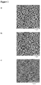
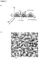
- AFM Atomic-Force-Microscopy
- the pores have an average diameter of about 200 nm and an average height of about 90 nm.
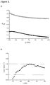
- the effective refractive index of the resulting anti-reflection LCP layers was evaluated, at optical wavelengths between 400 nm and 1000 nm, using a Variable Angle Spectroscopic Ellipsometer (V. A. S. E. from J. A. Woolam Co., Inc. Research & Instrumentation, Lincoln, NE USA). An example of the results is shown in Fig. 2-a (solid squares).
- a mixture Mix2 was made from:
- a 7.8 wt% solution of the mixture Mix2 was made in ethyl acetate, then homogenized with moderate stirring for 15 min using ultrasonic vibrations (with a Sonifier (trade mark) "W-250" digital by BRANSON Ultrasonics Corporation), and filtered trough a 0.2 ⁇ m filter.
- the solution was then thinly spin coated at 3000 rpm onto glass plates.
- the layers were then irradiated for 5 minutes under nitrogen at room temperature using isotropic (non-polarized) light from a mercury lamp at an intensity in the ultraviolet of 4.5 mW/cm 2 to crosslink the LCP monomers.
- the layers were optically transparent. Finally, the layers were rinsed with a solvent to remove the non cross-linked material.
- the layers were still transparent.
- the total thickness of the resulting anti-reflection LCP layer was about 120 nm.
- the layers were found to contain nano-pores.
- the pores have an average diameter of about 180 nm and an average height of about 120 nm (see Fig. 1-b ).
- the transmission of the resulting nano-porous LCP layer was evaluated, at optical wavelengths between 400 nm and 1000 nm, using a Variable Angle Spectroscopic Ellipsometer (V. A. S. E. from J. A. Woolam Co., Inc. Research & Instrumentation, Lincoln, NE USA).
- the results showed the high-performance anti-reflection of the LCP layers with zero % reflection in a wide wavelength region of the visible light (cf Fig. 2-b ).
- Example 3 Again varying the component ratio
- a mixture Mix3 was made from:
- a 4.7 wt% solution of the mixture Mix3 was made in ethyl acetate, then homogenized with moderate stirring for 30 min at 50 °C, and filtered through a 0.2 ⁇ m filter. The solution was then thinly spin coated at 1000 rpm onto glass plates. The layers were then irradiated for 5 minutes under nitrogen at room temperature using isotropic (non-polarized) light from a mercury lamp at an intensity in the ultraviolet of 4.5 mW/cm 2 . After this irradiation, the LCP monomers had become cross-linked. The layers were optically transparent. Finally, the layers were rinsed with ethyl acetate to remove the non cross-linked material. After this procedure, the layers were still transparent.
- the total thickness of the resulting anti-reflection LCP layer was about 120 nm.
- the layers were found to contain nano-pores.
- the pores have an average diameter of about 100 nm and an average height of about 50 nm (see Fig. 1-c ).
- Example 4 Preparation of an LCP layer on an orientation layer, leading to a modulated profile "nano-grooved" topological structure
- a 2 % solution of the photo-orienting material JP 265 (commercially available from CIBA), which is a linearly photo-polymerizable polymer (LPP), in cyclopentanone was thinly spin coated at 3000 rpm onto glass plates. The plates were warmed for 10 minutes at 180 °C on a hotplate. The resulting layer had a thickness of about 60 nm and was then
Landscapes
- Physics & Mathematics (AREA)
- Chemical & Material Sciences (AREA)
- General Physics & Mathematics (AREA)
- Optics & Photonics (AREA)
- Engineering & Computer Science (AREA)
- Crystallography & Structural Chemistry (AREA)
- Nonlinear Science (AREA)
- Materials Engineering (AREA)
- Organic Chemistry (AREA)
- Spectroscopy & Molecular Physics (AREA)
- Mathematical Physics (AREA)
- Nanotechnology (AREA)
- Manufacturing & Machinery (AREA)
- Mechanical Engineering (AREA)
- Composite Materials (AREA)
- Condensed Matter Physics & Semiconductors (AREA)
- Polarising Elements (AREA)
- Surface Treatment Of Optical Elements (AREA)
- Materials For Medical Uses (AREA)
- Optical Elements Other Than Lenses (AREA)
- Laminated Bodies (AREA)
Claims (5)
- Ein Verfahren zur Herstellung einer Nachbildung eines anisotrop topologisch strukturierten Polymerfilms oder Beschichtung, wobei der anisotrop topologisch strukturierte Polymerfilm oder Beschichtung als Kopiervorlage verwendet wird, wobei das Verfahren umfasst- Mischen mindestens zweier Materialien, wobeiein Material flüssigkristallin und nicht vernetzbar ist undein anderes Material vernetzbar und flüssigkristallin ist, enthaltend Moleküle mit Stäbchen-förmiger Gestalt, und das zu ¼ bis 4 Gewichtsanteilen pro Gewichtsanteil des nicht vernetzbaren, flüssigkristallinen Materials vorliegt,- Auftragen der Mischung auf ein Substrat,- Vernetzen des vernetzbaren Materials mittels Lichteinwirkung, wobei während des Vernetzens das vernetzbare Material in einem orientierten Zustand beibehalten wird, der durch eine unterliegende Orientierungsschicht auferlegt wird,- Entfernen des einen der Materialien unter Verwendung eines Lösungsmittels, welches gegenüber dem anderen Material inaktiv ist, um den topologisch strukturierten Polymerfilm oder Beschichtung zu bilden,- Auftragen des Materials für die Nachbildung auf den anisotrop topologisch strukturierten Film oder Beschichtung und Trennen des Materials von dem unterliegenden Film oder Beschichtung, wobei das nachgebildete Material ausgewählt ist aus der Gruppe: Metalle, Vorpolymere, Polymere, Dielektrika.
- Ein Verfahren zur Herstellung einer Nachbildung einer anisotrop topologischen Struktur, dadurch gekennzeichnet, dass die anisotrop topologische Struktur eine gemäß Anspruch 1 gefertigte Nachbildung ist.
- Ein Verfahren gemäß Anspruch 1, wobei die unterliegende Orientierungsschicht eine foto-orientierte Schicht ist.
- Ein Verfahren gemäß Anspruch 1, wobei das nicht vernetzbare Material ein oberflächenaktives Agens enthält.
- Ein Verfahren gemäß Anspruch 1, wobei der Film oder die Beschichtung als optischer Diffusor wirkt.
Applications Claiming Priority (3)
| Application Number | Priority Date | Filing Date | Title |
|---|---|---|---|
| GBGB9924746.2A GB9924746D0 (en) | 1999-10-19 | 1999-10-19 | Topologically structured polymer coating |
| GBGB9925458.3A GB9925458D0 (en) | 1999-10-27 | 1999-10-27 | Topologically structured polymer coating |
| EP00965716A EP1230319B1 (de) | 1999-10-19 | 2000-10-18 | Topologischstrukturierte polymerbeschichtung |
Related Parent Applications (1)
| Application Number | Title | Priority Date | Filing Date |
|---|---|---|---|
| EP00965716A Division EP1230319B1 (de) | 1999-10-19 | 2000-10-18 | Topologischstrukturierte polymerbeschichtung |
Publications (2)
| Publication Number | Publication Date |
|---|---|
| EP2014739A1 EP2014739A1 (de) | 2009-01-14 |
| EP2014739B1 true EP2014739B1 (de) | 2016-09-14 |
Family
ID=26316015
Family Applications (2)
| Application Number | Title | Priority Date | Filing Date |
|---|---|---|---|
| EP08105038.7A Expired - Lifetime EP2014739B1 (de) | 1999-10-19 | 2000-10-18 | Verfahren zur Herstellung einer Nachbildung eines anisotropisch topologisch strukturierten Polymer-Films oder Beschichtung |
| EP00965716A Expired - Lifetime EP1230319B1 (de) | 1999-10-19 | 2000-10-18 | Topologischstrukturierte polymerbeschichtung |
Family Applications After (1)
| Application Number | Title | Priority Date | Filing Date |
|---|---|---|---|
| EP00965716A Expired - Lifetime EP1230319B1 (de) | 1999-10-19 | 2000-10-18 | Topologischstrukturierte polymerbeschichtung |
Country Status (10)
| Country | Link |
|---|---|
| US (3) | US20070020404A1 (de) |
| EP (2) | EP2014739B1 (de) |
| JP (1) | JP4928038B2 (de) |
| KR (1) | KR100843639B1 (de) |
| CN (1) | CN1220754C (de) |
| AT (1) | ATE405623T1 (de) |
| AU (1) | AU7638600A (de) |
| DE (1) | DE60040011D1 (de) |
| HK (1) | HK1044960A1 (de) |
| WO (1) | WO2001029148A1 (de) |
Families Citing this family (73)
| Publication number | Priority date | Publication date | Assignee | Title |
|---|---|---|---|---|
| CA2445080A1 (en) * | 2001-04-24 | 2002-10-31 | Merck Patent Gesellschaft Mit Beschraenkter Haftung | Birefringent marking |
| TW557368B (en) * | 2001-06-29 | 2003-10-11 | Jsr Corp | Anti-reflection film laminated body and method of manufacturing the laminated body |
| AU2002357842A1 (en) * | 2001-12-13 | 2003-06-23 | E Ink Corporation | Electrophoretic electronic displays with films having a low index of refraction |
| JP3785093B2 (ja) * | 2001-12-28 | 2006-06-14 | アルプス電気株式会社 | 導光板、その製造方法、照明装置、及び液晶表示装置 |
| EP1363143A1 (de) * | 2002-05-17 | 2003-11-19 | Rolic AG | Helle und weisse optische Streuschicht |
| DE10241708B4 (de) * | 2002-09-09 | 2005-09-29 | Fraunhofer-Gesellschaft zur Förderung der angewandten Forschung e.V. | Verfahren zur Reduzierung der Grenzflächenreflexion von Kunststoffsubstraten sowie derart modifiziertes Substrat und dessen Verwendung |
| EP1400838A1 (de) * | 2002-09-19 | 2004-03-24 | Rolic AG | Dünnschichten mit geriffelter Oberflächentopologie und Herstellungsverfahren |
| EP1418448A1 (de) | 2002-11-06 | 2004-05-12 | Koninklijke DSM N.V. | Herstellung einer mechanisch haltbaren, einlagigen Beschichtung mit Antireflex-Eigenschaften |
| JP2004177806A (ja) * | 2002-11-28 | 2004-06-24 | Alps Electric Co Ltd | 反射防止構造および照明装置と液晶表示装置並びに反射防止膜成型用金型 |
| TWI289708B (en) | 2002-12-25 | 2007-11-11 | Qualcomm Mems Technologies Inc | Optical interference type color display |
| DE10318566B4 (de) * | 2003-04-15 | 2005-11-17 | Fresnel Optics Gmbh | Verfahren und Werkzeug zur Herstellung transparenter optischer Elemente aus polymeren Werkstoffen |
| DE10324050A1 (de) * | 2003-05-27 | 2004-12-30 | Infineon Technologies Ag | Schichtstapel und Verfahren zur Herstellung eines Schichtstapels |
| US7342705B2 (en) | 2004-02-03 | 2008-03-11 | Idc, Llc | Spatial light modulator with integrated optical compensation structure |
| US7088510B2 (en) * | 2004-02-23 | 2006-08-08 | Jds Uniphase Corporation | Anti-aliasing optical filter for image sensors |
| US20050260334A1 (en) * | 2004-05-24 | 2005-11-24 | The Hong Kong Univerisity Of Science And Technology | Method of achieving high pretilt angles in a lilquid crystal cell |
| US7378136B2 (en) * | 2004-07-09 | 2008-05-27 | 3M Innovative Properties Company | Optical film coating |
| EP1771752B1 (de) * | 2004-07-21 | 2020-10-07 | ROLIC Technologies AG | Anisotrope optische einrichtung und herstellungsverfahren dafür |
| US7170666B2 (en) * | 2004-07-27 | 2007-01-30 | Hewlett-Packard Development Company, L.P. | Nanostructure antireflection surfaces |
| EP1645893A1 (de) * | 2004-10-08 | 2006-04-12 | Fraunhofer-Gesellschaft zur Förderung der angewandten Forschung e.V. | Beugungsgitter für elektromagnetische Strahlung sowie Verfahren zur Herstellung |
| US20070065638A1 (en) * | 2005-09-20 | 2007-03-22 | Eastman Kodak Company | Nano-structured thin film with reduced light reflection |
| US20090225424A1 (en) * | 2005-09-30 | 2009-09-10 | Fabian Zimmer | Micro-optical diffraction grid and process for producing the same |
| US10591651B2 (en) | 2005-09-30 | 2020-03-17 | Hiperscan Gmbh | Micro-optical electromagnetic radiation diffraction grating and method for manufacture |
| KR100738104B1 (ko) | 2006-02-08 | 2007-07-12 | 삼성전자주식회사 | 편광 도광판 및 그 제조 방법 및 상기 편광 도광판을이용한 평판표시장치용 조명장치 |
| US8134660B2 (en) | 2006-03-13 | 2012-03-13 | Dai Nippon Printing Co., Ltd. | Optical diffusion device, projection screen, design member and security medium |
| EP1855127A1 (de) * | 2006-05-12 | 2007-11-14 | Rolic AG | Optisch wirksame Oberflächenreliefmikrostrukturen und Verfahren zu ihrer Herstellung |
| ATE426184T1 (de) | 2006-05-31 | 2009-04-15 | Suisse Electronique Microtech | Nanostrukturierter diffraktionsfilter nullter ordnung |
| ATE556272T1 (de) | 2006-10-06 | 2012-05-15 | Qualcomm Mems Technologies Inc | Optische verluststruktur in einer beleuchtungsvorrichtung |
| WO2008045312A1 (en) * | 2006-10-06 | 2008-04-17 | Qualcomm Mems Technologies, Inc. | Apparatus and method for reducing back reflection from an illumination device |
| KR20080097554A (ko) * | 2007-05-02 | 2008-11-06 | 삼성전자주식회사 | 플리커 튜닝 방법, 이를 수행하기 위한 플리커 튜닝 회로및 이를 구비한 표시 장치 |
| EP2012173A3 (de) * | 2007-07-03 | 2009-12-09 | JDS Uniphase Corporation | Ungeätzte flache polarisations-selektive optische Diffraktionselemente |
| US8643822B2 (en) * | 2007-07-03 | 2014-02-04 | Jds Uniphase Corporation | Non-etched flat polarization-selective diffractive optical elements |
| DE102007052952A1 (de) * | 2007-10-31 | 2009-05-07 | Bundesdruckerei Gmbh | Verfahren und Vorrichtung zur Herstellung von Hologrammen mit wasserzeichenartiger Struktur |
| US8941631B2 (en) | 2007-11-16 | 2015-01-27 | Qualcomm Mems Technologies, Inc. | Simultaneous light collection and illumination on an active display |
| DE102008029158A1 (de) * | 2007-12-21 | 2009-06-25 | Giesecke & Devrient Gmbh | Sicherheitselement |
| US8059232B2 (en) * | 2008-02-08 | 2011-11-15 | Motorola Mobility, Inc. | Electronic device and LC shutter for polarization-sensitive switching between transparent and diffusive states |
| DE102008018866A1 (de) * | 2008-04-15 | 2009-10-22 | Fraunhofer-Gesellschaft zur Förderung der angewandten Forschung e.V. | Reflexionsminderndes Interferenzschichtsystem und Verfahren zu dessen Herstellung |
| EP2264488B1 (de) | 2008-04-18 | 2016-12-28 | Toppan Printing Co., Ltd. | Kennzeichnungsmaterial und gekennzeichneter warenposten |
| WO2010051149A1 (en) * | 2008-10-27 | 2010-05-06 | Arkema France | Nano-structure coated sheets/films for optical electronic displays and photovoltaic modules |
| JP2012517919A (ja) * | 2009-02-18 | 2012-08-09 | ロリク アーゲー | 表面レリーフ微細構造、関連するデバイスおよびそれらを作製する方法 |
| US8808811B2 (en) | 2009-04-15 | 2014-08-19 | 3M Innovative Properties Company | Process and apparatus for a nanovoided article |
| US8534849B2 (en) | 2009-04-15 | 2013-09-17 | 3M Innovative Properties Company | Retroreflecting optical construction |
| TWI605276B (zh) | 2009-04-15 | 2017-11-11 | 3M新設資產公司 | 光學結構及包含該光學結構之顯示系統 |
| CN102449508B (zh) | 2009-04-15 | 2014-12-17 | 3M创新有限公司 | 光学膜 |
| US9464179B2 (en) | 2009-04-15 | 2016-10-11 | 3M Innovative Properties Company | Process and apparatus for a nanovoided article |
| US9291752B2 (en) | 2013-08-19 | 2016-03-22 | 3M Innovative Properties Company | Retroreflecting optical construction |
| CN102460244B (zh) | 2009-04-15 | 2014-11-19 | 3M创新有限公司 | 具有包括空隙的光学膜的光导和用于显示系统的背光源 |
| WO2010120871A1 (en) | 2009-04-15 | 2010-10-21 | 3M Innovative Properties Company | Optical film for preventing optical coupling |
| WO2010138765A1 (en) | 2009-05-29 | 2010-12-02 | Qualcomm Mems Technologies, Inc. | Illumination devices and methods of fabrication thereof |
| JP4645772B1 (ja) * | 2009-10-09 | 2011-03-09 | ソニー株式会社 | 位相差素子用配向膜およびその製造方法、位相差素子およびその製造方法、表示装置 |
| EP2491445B1 (de) | 2009-10-24 | 2018-01-03 | 3M Innovative Properties Company | Lichtquelle und anzeigesystem damit |
| EP3730978A1 (de) | 2009-12-01 | 2020-10-28 | Toppan Printing Co., Ltd. | Anzeige und etikettierter artikel |
| EP2510389B1 (de) | 2009-12-08 | 2017-07-12 | 3M Innovative Properties Company | Optische konstruktionen mit einem lichtleiter und folien mit niedrigem brechungsindex |
| WO2011129831A1 (en) | 2010-04-15 | 2011-10-20 | 3M Innovative Properties Company | Retroreflective articles including optically active areas and optically inactive areas |
| JP5997132B2 (ja) | 2010-04-15 | 2016-09-28 | スリーエム イノベイティブ プロパティズ カンパニー | 再帰反射性物品及びその形成方法 |
| KR20130092396A (ko) | 2010-04-15 | 2013-08-20 | 쓰리엠 이노베이티브 프로퍼티즈 캄파니 | 광학적 활성 영역 및 광학적 불활성 영역을 포함하는 재귀반사성 물품 |
| GB2484068B (en) * | 2010-09-22 | 2012-09-12 | Au Optronics Corp | Liquid crystal coating film,method for manufacturing the same and method for manufacturing birefringent liquid crystal component |
| US8902484B2 (en) | 2010-12-15 | 2014-12-02 | Qualcomm Mems Technologies, Inc. | Holographic brightness enhancement film |
| US8828650B2 (en) | 2011-09-13 | 2014-09-09 | Far Eastern New Century Corporation | Method for making a retarder |
| US9939682B2 (en) | 2013-02-15 | 2018-04-10 | E-Vision, Llc | Liquid crystal alignment layers and method of fabrication |
| AT515640A1 (de) * | 2014-03-31 | 2015-10-15 | Werner Färber | Beleuchtungsvorrichtung |
| KR20160118437A (ko) * | 2015-04-01 | 2016-10-12 | 삼성디스플레이 주식회사 | 액정 표시 장치 및 그 제조 방법 |
| US11054551B2 (en) | 2015-04-16 | 2021-07-06 | Rolic Ag | Multiple image scattering device |
| WO2017025336A1 (en) | 2015-08-07 | 2017-02-16 | Rolic Ag | Azimuthally modulated scattering device |
| US10135034B1 (en) * | 2016-03-04 | 2018-11-20 | Apple Inc. | Display device with pixel-integrated black matrix and elliptical polarizer |
| JP6897238B2 (ja) * | 2017-03-31 | 2021-06-30 | 大日本印刷株式会社 | 光学フィルムおよび画像表示装置 |
| US11243333B1 (en) | 2018-10-24 | 2022-02-08 | Facebook Technologies, Llc | Nanovoided optical structures and corresponding systems and methods |
| US11526129B1 (en) | 2018-12-07 | 2022-12-13 | Meta Platforms Technologies, Llc | Nanovoided holographic structures and corresponding systems and methods |
| US11340386B1 (en) * | 2018-12-07 | 2022-05-24 | Facebook Technologies, Llc | Index-gradient structures with nanovoided materials and corresponding systems and methods |
| US11233189B2 (en) | 2018-12-11 | 2022-01-25 | Facebook Technologies, Llc | Nanovoided tunable birefringence |
| CN114341239B (zh) * | 2019-09-25 | 2023-04-21 | 富士胶片株式会社 | 液晶聚合物薄膜及其制造方法、挠性覆铜层叠板及挠性印制电路板 |
| CN111004508B (zh) * | 2019-11-11 | 2022-02-11 | 北京航空航天大学 | 一种亲水性单层多孔膜及其制备方法与应用 |
| CN114475043B (zh) * | 2020-11-11 | 2023-04-28 | 中钞特种防伪科技有限公司 | 光学防伪元件及其制作方法、防伪产品 |
| TW202247990A (zh) | 2021-05-12 | 2022-12-16 | 瑞士商羅立克科技股份公司 | 用於創造表面微結構的方法 |
Citations (1)
| Publication number | Priority date | Publication date | Assignee | Title |
|---|---|---|---|---|
| US5605727A (en) * | 1994-06-21 | 1997-02-25 | Thomson-Csf | Method for obtaining composite materials based on cross-linked polymer and fluid molecules, comprising a step of drying in supercritical phase |
Family Cites Families (37)
| Publication number | Priority date | Publication date | Assignee | Title |
|---|---|---|---|---|
| JPS5031845A (de) * | 1973-07-20 | 1975-03-28 | ||
| US4564658A (en) * | 1982-11-24 | 1986-01-14 | General Electric Company | Thermoplastic polyester-linear low density polyethylene molding compositions |
| GB2171549B (en) * | 1985-02-15 | 1988-05-18 | Citizen Watch Co Ltd | Liquid crystal display device |
| IL79884A (en) * | 1985-09-23 | 1990-11-05 | Gelman Sciences Inc | Microporous membrane laminate |
| JPH01131257A (ja) * | 1987-11-16 | 1989-05-24 | Oji Paper Co Ltd | 微多孔性高分子成形体の製造方法 |
| JPH0698666B2 (ja) * | 1988-03-15 | 1994-12-07 | 工業技術院長 | 多孔性液晶高分子シートの製造方法 |
| US4974941A (en) | 1989-03-08 | 1990-12-04 | Hercules Incorporated | Process of aligning and realigning liquid crystal media |
| JPH04121701A (ja) * | 1990-09-12 | 1992-04-22 | Canon Inc | 反射防止膜 |
| US5438421A (en) * | 1991-04-24 | 1995-08-01 | Alps Electric Co., Ltd. | Orientation film of liquid crystal having bilaterally asymmetric ridges separated by grooves |
| SG50586A1 (en) | 1991-07-26 | 2000-05-23 | Rolic Ag | Liquid crystal display cell |
| JPH063501A (ja) * | 1992-06-23 | 1994-01-14 | Dainippon Printing Co Ltd | 多孔質光学材料 |
| US5498450A (en) * | 1992-11-18 | 1996-03-12 | Fuji Xerox Co., Ltd. | Liquid crystal-polymer composite film, electro-optical element using the same, and process for producing electro-optical element |
| SG50569A1 (en) | 1993-02-17 | 2001-02-20 | Rolic Ag | Optical component |
| FR2702058B1 (fr) * | 1993-02-23 | 1995-04-07 | Thomson Csf | Procédé d'obtention de matériaux composites à base de polymère et de cristaux liquides avec colorants dichroiques. |
| KR0148391B1 (ko) * | 1993-08-31 | 1998-11-16 | 박경팔 | 액정표시소자 |
| GB9402516D0 (en) * | 1994-02-09 | 1994-03-30 | Secr Defence | Liquid crystal device alignment |
| US5717474A (en) * | 1994-09-30 | 1998-02-10 | Honeywell Inc. | Wide-viewing angle multi-domain halftone active matrix liquid crystal display having compensating retardation |
| US5847795A (en) * | 1995-07-27 | 1998-12-08 | Canon Kabushiki Kaisha | Liquid crystal display apparatus and anti-reflection film applicable thereto |
| JPH09171172A (ja) * | 1995-12-19 | 1997-06-30 | Fuji Xerox Co Ltd | 光学素子 |
| US5726723A (en) * | 1996-01-31 | 1998-03-10 | Technology Research International Corporation | Sub-twisted nematic liquid crystal display |
| KR100474780B1 (ko) * | 1997-02-07 | 2005-08-04 | 후지 샤신 필름 가부시기가이샤 | 광학보상시이트,그의제조방법및액정디스플레이 |
| US6175399B1 (en) * | 1997-02-10 | 2001-01-16 | Sharp Kabushiki Kaisha | Reflective type liquid crystal display device having a diffusion layer of phase separated liquid crystal and polymer |
| DE19705497C2 (de) * | 1997-02-13 | 1999-01-28 | Max Planck Gesellschaft | Verfahren zur Herstellung mesoporöser Feststoffe, durch das Verfahren erhältliche Feststoffe und deren Verwendung |
| DE19708776C1 (de) * | 1997-03-04 | 1998-06-18 | Fraunhofer Ges Forschung | Entspiegelungsschicht sowie Verfahren zur Herstellung derselben |
| JP3226830B2 (ja) * | 1997-03-31 | 2001-11-05 | 日本電気株式会社 | 液晶表示装置 |
| JPH10282305A (ja) * | 1997-04-01 | 1998-10-23 | Fuji Photo Film Co Ltd | 多孔質光学材料およびそれを用いた画像表示装置 |
| KR100238377B1 (ko) * | 1997-05-03 | 2000-01-15 | 김영환 | 광학배향장치 및 방법 |
| ES2392342T3 (es) * | 1997-05-09 | 2012-12-07 | Rolic Ag | Elemento óptico que comprende un retardador estructurado |
| JPH10333133A (ja) * | 1997-05-29 | 1998-12-18 | Teijin Ltd | 反射型液晶表示装置 |
| KR100247640B1 (ko) * | 1997-06-27 | 2000-03-15 | 김영환 | 액정 표시 소자 및 그 제조방법 |
| JPH1195195A (ja) | 1997-09-17 | 1999-04-09 | Sharp Corp | 高分子分散型液晶表示装置およびその製造方法 |
| US7369327B1 (en) * | 1998-06-09 | 2008-05-06 | Olympus Corporation | Variable optical-property element and optical apparatus including the same |
| GB9812636D0 (en) | 1998-06-11 | 1998-08-12 | Rolic Ag | Optical component orientation layer and layerable polymerisable mixture |
| GB9902402D0 (en) * | 1999-02-03 | 1999-03-24 | Rolic Ag | Method of imparting preferred alignment, and liquid crystal device elements incorporating a preferred alignment |
| US6278552B1 (en) * | 1999-05-12 | 2001-08-21 | Minolta Co., Ltd. | Polarization separation device and projection-type display apparatus |
| KR20010077785A (ko) * | 2000-02-08 | 2001-08-20 | 구본준, 론 위라하디락사 | 액정표시장치용 기판 러빙방법 |
| KR20090082101A (ko) * | 2006-11-21 | 2009-07-29 | 소니 가부시끼 가이샤 | 액정 표시 패널 및 액정 표시 패널의 제조 방법 |
-
2000
- 2000-10-18 JP JP2001531936A patent/JP4928038B2/ja not_active Expired - Fee Related
- 2000-10-18 AU AU76386/00A patent/AU7638600A/en not_active Abandoned
- 2000-10-18 AT AT00965716T patent/ATE405623T1/de not_active IP Right Cessation
- 2000-10-18 EP EP08105038.7A patent/EP2014739B1/de not_active Expired - Lifetime
- 2000-10-18 KR KR1020027004888A patent/KR100843639B1/ko active IP Right Grant
- 2000-10-18 WO PCT/CH2000/000562 patent/WO2001029148A1/en active IP Right Grant
- 2000-10-18 CN CNB008135991A patent/CN1220754C/zh not_active Expired - Fee Related
- 2000-10-18 DE DE60040011T patent/DE60040011D1/de not_active Expired - Lifetime
- 2000-10-18 EP EP00965716A patent/EP1230319B1/de not_active Expired - Lifetime
-
2002
- 2002-09-04 HK HK02106524.0A patent/HK1044960A1/zh unknown
-
2006
- 2006-09-06 US US11/515,736 patent/US20070020404A1/en not_active Abandoned
-
2009
- 2009-01-21 US US12/357,318 patent/US8906458B2/en not_active Expired - Fee Related
-
2014
- 2014-11-04 US US14/532,328 patent/US20150125664A1/en not_active Abandoned
Patent Citations (1)
| Publication number | Priority date | Publication date | Assignee | Title |
|---|---|---|---|---|
| US5605727A (en) * | 1994-06-21 | 1997-02-25 | Thomson-Csf | Method for obtaining composite materials based on cross-linked polymer and fluid molecules, comprising a step of drying in supercritical phase |
Also Published As
| Publication number | Publication date |
|---|---|
| ATE405623T1 (de) | 2008-09-15 |
| DE60040011D1 (de) | 2008-10-02 |
| AU7638600A (en) | 2001-04-30 |
| EP2014739A1 (de) | 2009-01-14 |
| US20070020404A1 (en) | 2007-01-25 |
| WO2001029148A1 (en) | 2001-04-26 |
| US20090136687A1 (en) | 2009-05-28 |
| CN1220754C (zh) | 2005-09-28 |
| CN1377399A (zh) | 2002-10-30 |
| JP4928038B2 (ja) | 2012-05-09 |
| EP1230319A1 (de) | 2002-08-14 |
| US8906458B2 (en) | 2014-12-09 |
| US20150125664A1 (en) | 2015-05-07 |
| HK1044960A1 (zh) | 2002-11-08 |
| JP2003512641A (ja) | 2003-04-02 |
| KR20020042872A (ko) | 2002-06-07 |
| EP1230319B1 (de) | 2008-08-20 |
| KR100843639B1 (ko) | 2008-07-07 |
Similar Documents
| Publication | Publication Date | Title |
|---|---|---|
| EP2014739B1 (de) | Verfahren zur Herstellung einer Nachbildung eines anisotropisch topologisch strukturierten Polymer-Films oder Beschichtung | |
| Ibn-Elhaj et al. | Optical polymer thin films with isotropic and anisotropic nano-corrugated surface topologies | |
| JP4647782B2 (ja) | 光学部材、配向層及び層状化可能な重合性混合物 | |
| AU2005263239B2 (en) | Anisotropic optical devices and method for making same | |
| JP4054071B2 (ja) | 液晶異方性層を有する層状光学的構成部品 | |
| Lim et al. | Anisotropic nano-imprinting technique for fabricating a patterned optical film of a liquid crystalline polymer | |
| Broer | Creation of supramolecular thin film architectures with liquid-crystalline networks | |
| EP1094103A1 (de) | Topologisch strukturierte Polymerbeschichtung | |
| EP1157302B1 (de) | Verfahren zur herstellung eines flüssigkristallpolymerelementes | |
| EP1363143A1 (de) | Helle und weisse optische Streuschicht | |
| JP2005049866A (ja) | 位相差層およびそれを用いた液晶表示装置 | |
| EP1400838A1 (de) | Dünnschichten mit geriffelter Oberflächentopologie und Herstellungsverfahren | |
| EP1147451B1 (de) | Verfahren zum erzeugen einer bevorzugten ausrichtung in flüssigkristallzellen | |
| TW593641B (en) | Topologically structured polymer coating | |
| GB2324881A (en) | Patterned optical elements | |
| Sim et al. | Self-organized wrinkling of liquid crystalline polymer with plasma treatment | |
| Zhao | Patterned and Photo-induced Vertical Alignment for Liquid Crystal Photonics and Display Applications | |
| Ibn-Elhaj et al. | Nano-and Micro-Corrugations in Photo-Aligned Polymer Thin-Films; Correlations Between Topologies and Directional Light Scattering | |
| Kossyrev | Tailored molecular order in reactive mesogens |
Legal Events
| Date | Code | Title | Description |
|---|---|---|---|
| PUAI | Public reference made under article 153(3) epc to a published international application that has entered the european phase |
Free format text: ORIGINAL CODE: 0009012 |
|
| AC | Divisional application: reference to earlier application |
Ref document number: 1230319 Country of ref document: EP Kind code of ref document: P |
|
| AK | Designated contracting states |
Kind code of ref document: A1 Designated state(s): AT BE CH CY DE DK ES FI FR GB GR IE IT LI LU MC NL PT SE |
|
| 17P | Request for examination filed |
Effective date: 20090714 |
|
| 17Q | First examination report despatched |
Effective date: 20090811 |
|
| AKX | Designation fees paid |
Designated state(s): AT BE CH CY DE DK ES FI FR GB GR IE IT LI LU MC NL PT SE |
|
| REG | Reference to a national code |
Ref country code: DE Ref legal event code: R079 Ref document number: 60049461 Country of ref document: DE Free format text: PREVIOUS MAIN CLASS: C09K0019540000 Ipc: B82Y0030000000 |
|
| GRAP | Despatch of communication of intention to grant a patent |
Free format text: ORIGINAL CODE: EPIDOSNIGR1 |
|
| RIC1 | Information provided on ipc code assigned before grant |
Ipc: G02B 1/11 20150101ALI20160523BHEP Ipc: B29C 41/00 20060101ALI20160523BHEP Ipc: G02B 5/30 20060101ALI20160523BHEP Ipc: B05D 5/06 20060101ALI20160523BHEP Ipc: G02B 1/08 20060101ALI20160523BHEP Ipc: B82Y 30/00 20110101AFI20160523BHEP Ipc: C09K 19/54 20060101ALI20160523BHEP Ipc: G02B 5/18 20060101ALI20160523BHEP Ipc: G02B 5/02 20060101ALI20160523BHEP Ipc: G02F 1/1337 20060101ALI20160523BHEP Ipc: G02F 1/139 20060101ALI20160523BHEP Ipc: C09K 19/56 20060101ALI20160523BHEP |
|
| INTG | Intention to grant announced |
Effective date: 20160622 |
|
| GRAS | Grant fee paid |
Free format text: ORIGINAL CODE: EPIDOSNIGR3 |
|
| GRAA | (expected) grant |
Free format text: ORIGINAL CODE: 0009210 |
|
| AC | Divisional application: reference to earlier application |
Ref document number: 1230319 Country of ref document: EP Kind code of ref document: P |
|
| AK | Designated contracting states |
Kind code of ref document: B1 Designated state(s): AT BE CH CY DE DK ES FI FR GB GR IE IT LI LU MC NL PT SE |
|
| REG | Reference to a national code |
Ref country code: GB Ref legal event code: FG4D |
|
| REG | Reference to a national code |
Ref country code: CH Ref legal event code: EP |
|
| REG | Reference to a national code |
Ref country code: IE Ref legal event code: FG4D |
|
| REG | Reference to a national code |
Ref country code: AT Ref legal event code: REF Ref document number: 828749 Country of ref document: AT Kind code of ref document: T Effective date: 20161015 |
|
| REG | Reference to a national code |
Ref country code: FR Ref legal event code: PLFP Year of fee payment: 17 |
|
| REG | Reference to a national code |
Ref country code: DE Ref legal event code: R096 Ref document number: 60049461 Country of ref document: DE |
|
| REG | Reference to a national code |
Ref country code: NL Ref legal event code: FP |
|
| PG25 | Lapsed in a contracting state [announced via postgrant information from national office to epo] |
Ref country code: FI Free format text: LAPSE BECAUSE OF FAILURE TO SUBMIT A TRANSLATION OF THE DESCRIPTION OR TO PAY THE FEE WITHIN THE PRESCRIBED TIME-LIMIT Effective date: 20160914 |
|
| REG | Reference to a national code |
Ref country code: AT Ref legal event code: MK05 Ref document number: 828749 Country of ref document: AT Kind code of ref document: T Effective date: 20160914 |
|
| PG25 | Lapsed in a contracting state [announced via postgrant information from national office to epo] |
Ref country code: BE Free format text: LAPSE BECAUSE OF NON-PAYMENT OF DUE FEES Effective date: 20161031 Ref country code: SE Free format text: LAPSE BECAUSE OF FAILURE TO SUBMIT A TRANSLATION OF THE DESCRIPTION OR TO PAY THE FEE WITHIN THE PRESCRIBED TIME-LIMIT Effective date: 20160914 Ref country code: ES Free format text: LAPSE BECAUSE OF FAILURE TO SUBMIT A TRANSLATION OF THE DESCRIPTION OR TO PAY THE FEE WITHIN THE PRESCRIBED TIME-LIMIT Effective date: 20160914 Ref country code: GR Free format text: LAPSE BECAUSE OF FAILURE TO SUBMIT A TRANSLATION OF THE DESCRIPTION OR TO PAY THE FEE WITHIN THE PRESCRIBED TIME-LIMIT Effective date: 20161215 |
|
| PG25 | Lapsed in a contracting state [announced via postgrant information from national office to epo] |
Ref country code: AT Free format text: LAPSE BECAUSE OF FAILURE TO SUBMIT A TRANSLATION OF THE DESCRIPTION OR TO PAY THE FEE WITHIN THE PRESCRIBED TIME-LIMIT Effective date: 20160914 Ref country code: PT Free format text: LAPSE BECAUSE OF FAILURE TO SUBMIT A TRANSLATION OF THE DESCRIPTION OR TO PAY THE FEE WITHIN THE PRESCRIBED TIME-LIMIT Effective date: 20170116 Ref country code: BE Free format text: LAPSE BECAUSE OF FAILURE TO SUBMIT A TRANSLATION OF THE DESCRIPTION OR TO PAY THE FEE WITHIN THE PRESCRIBED TIME-LIMIT Effective date: 20160914 |
|
| REG | Reference to a national code |
Ref country code: DE Ref legal event code: R097 Ref document number: 60049461 Country of ref document: DE |
|
| PG25 | Lapsed in a contracting state [announced via postgrant information from national office to epo] |
Ref country code: IT Free format text: LAPSE BECAUSE OF FAILURE TO SUBMIT A TRANSLATION OF THE DESCRIPTION OR TO PAY THE FEE WITHIN THE PRESCRIBED TIME-LIMIT Effective date: 20160914 |
|
| PLBE | No opposition filed within time limit |
Free format text: ORIGINAL CODE: 0009261 |
|
| STAA | Information on the status of an ep patent application or granted ep patent |
Free format text: STATUS: NO OPPOSITION FILED WITHIN TIME LIMIT |
|
| REG | Reference to a national code |
Ref country code: IE Ref legal event code: MM4A |
|
| PG25 | Lapsed in a contracting state [announced via postgrant information from national office to epo] |
Ref country code: DK Free format text: LAPSE BECAUSE OF FAILURE TO SUBMIT A TRANSLATION OF THE DESCRIPTION OR TO PAY THE FEE WITHIN THE PRESCRIBED TIME-LIMIT Effective date: 20160914 |
|
| 26N | No opposition filed |
Effective date: 20170615 |
|
| PG25 | Lapsed in a contracting state [announced via postgrant information from national office to epo] |
Ref country code: LU Free format text: LAPSE BECAUSE OF NON-PAYMENT OF DUE FEES Effective date: 20161018 |
|
| REG | Reference to a national code |
Ref country code: FR Ref legal event code: PLFP Year of fee payment: 18 |
|
| PG25 | Lapsed in a contracting state [announced via postgrant information from national office to epo] |
Ref country code: IE Free format text: LAPSE BECAUSE OF NON-PAYMENT OF DUE FEES Effective date: 20161018 |
|
| REG | Reference to a national code |
Ref country code: CH Ref legal event code: PFUS Owner name: ROLIC TECHNOLOGIES AG, CH Free format text: FORMER OWNER: ROLIC AG, CH |
|
| PG25 | Lapsed in a contracting state [announced via postgrant information from national office to epo] |
Ref country code: CY Free format text: LAPSE BECAUSE OF FAILURE TO SUBMIT A TRANSLATION OF THE DESCRIPTION OR TO PAY THE FEE WITHIN THE PRESCRIBED TIME-LIMIT Effective date: 20160914 |
|
| PG25 | Lapsed in a contracting state [announced via postgrant information from national office to epo] |
Ref country code: MC Free format text: LAPSE BECAUSE OF FAILURE TO SUBMIT A TRANSLATION OF THE DESCRIPTION OR TO PAY THE FEE WITHIN THE PRESCRIBED TIME-LIMIT Effective date: 20160914 |
|
| REG | Reference to a national code |
Ref country code: FR Ref legal event code: PLFP Year of fee payment: 19 |
|
| PGFP | Annual fee paid to national office [announced via postgrant information from national office to epo] |
Ref country code: NL Payment date: 20181019 Year of fee payment: 19 |
|
| PGFP | Annual fee paid to national office [announced via postgrant information from national office to epo] |
Ref country code: CH Payment date: 20181019 Year of fee payment: 19 Ref country code: GB Payment date: 20181019 Year of fee payment: 19 Ref country code: FR Payment date: 20181022 Year of fee payment: 19 |
|
| PGFP | Annual fee paid to national office [announced via postgrant information from national office to epo] |
Ref country code: DE Payment date: 20191021 Year of fee payment: 20 |
|
| REG | Reference to a national code |
Ref country code: CH Ref legal event code: PL |
|
| REG | Reference to a national code |
Ref country code: NL Ref legal event code: MM Effective date: 20191101 |
|
| PG25 | Lapsed in a contracting state [announced via postgrant information from national office to epo] |
Ref country code: CH Free format text: LAPSE BECAUSE OF NON-PAYMENT OF DUE FEES Effective date: 20191031 Ref country code: LI Free format text: LAPSE BECAUSE OF NON-PAYMENT OF DUE FEES Effective date: 20191031 |
|
| PG25 | Lapsed in a contracting state [announced via postgrant information from national office to epo] |
Ref country code: NL Free format text: LAPSE BECAUSE OF NON-PAYMENT OF DUE FEES Effective date: 20191101 |
|
| GBPC | Gb: european patent ceased through non-payment of renewal fee |
Effective date: 20191018 |
|
| REG | Reference to a national code |
Ref country code: DE Ref legal event code: R071 Ref document number: 60049461 Country of ref document: DE |
|
| PG25 | Lapsed in a contracting state [announced via postgrant information from national office to epo] |
Ref country code: FR Free format text: LAPSE BECAUSE OF NON-PAYMENT OF DUE FEES Effective date: 20191031 Ref country code: GB Free format text: LAPSE BECAUSE OF NON-PAYMENT OF DUE FEES Effective date: 20191018 |