EP2009686B1 - Tiefgrabenisolationsstrukturen in integrierten Halbleiterbauelementen - Google Patents
Tiefgrabenisolationsstrukturen in integrierten Halbleiterbauelementen Download PDFInfo
- Publication number
- EP2009686B1 EP2009686B1 EP07012746A EP07012746A EP2009686B1 EP 2009686 B1 EP2009686 B1 EP 2009686B1 EP 07012746 A EP07012746 A EP 07012746A EP 07012746 A EP07012746 A EP 07012746A EP 2009686 B1 EP2009686 B1 EP 2009686B1
- Authority
- EP
- European Patent Office
- Prior art keywords
- layer
- trench
- conductivity type
- forming
- layers
- Prior art date
- Legal status (The legal status is an assumption and is not a legal conclusion. Google has not performed a legal analysis and makes no representation as to the accuracy of the status listed.)
- Not-in-force
Links
Images


Classifications
-
- H—ELECTRICITY
- H10—SEMICONDUCTOR DEVICES; ELECTRIC SOLID-STATE DEVICES NOT OTHERWISE PROVIDED FOR
- H10P—GENERIC PROCESSES OR APPARATUS FOR THE MANUFACTURE OR TREATMENT OF DEVICES COVERED BY CLASS H10
- H10P90/00—Preparation of wafers not covered by a single main group of this subclass, e.g. wafer reinforcement
- H10P90/19—Preparing inhomogeneous wafers
- H10P90/1904—Preparing vertically inhomogeneous wafers
- H10P90/1906—Preparing SOI wafers
-
- H—ELECTRICITY
- H10—SEMICONDUCTOR DEVICES; ELECTRIC SOLID-STATE DEVICES NOT OTHERWISE PROVIDED FOR
- H10W—GENERIC PACKAGES, INTERCONNECTIONS, CONNECTORS OR OTHER CONSTRUCTIONAL DETAILS OF DEVICES COVERED BY CLASS H10
- H10W10/00—Isolation regions in semiconductor bodies between components of integrated devices
- H10W10/01—Manufacture or treatment
- H10W10/011—Manufacture or treatment of isolation regions comprising dielectric materials
- H10W10/014—Manufacture or treatment of isolation regions comprising dielectric materials using trench refilling with dielectric materials, e.g. shallow trench isolations
- H10W10/0148—Manufacture or treatment of isolation regions comprising dielectric materials using trench refilling with dielectric materials, e.g. shallow trench isolations comprising introducing impurities in side walls or bottom walls of trenches, e.g. for forming channel stoppers
-
- H—ELECTRICITY
- H10—SEMICONDUCTOR DEVICES; ELECTRIC SOLID-STATE DEVICES NOT OTHERWISE PROVIDED FOR
- H10W—GENERIC PACKAGES, INTERCONNECTIONS, CONNECTORS OR OTHER CONSTRUCTIONAL DETAILS OF DEVICES COVERED BY CLASS H10
- H10W10/00—Isolation regions in semiconductor bodies between components of integrated devices
- H10W10/01—Manufacture or treatment
- H10W10/031—Manufacture or treatment of isolation regions comprising PN junctions
-
- H—ELECTRICITY
- H10—SEMICONDUCTOR DEVICES; ELECTRIC SOLID-STATE DEVICES NOT OTHERWISE PROVIDED FOR
- H10W—GENERIC PACKAGES, INTERCONNECTIONS, CONNECTORS OR OTHER CONSTRUCTIONAL DETAILS OF DEVICES COVERED BY CLASS H10
- H10W10/00—Isolation regions in semiconductor bodies between components of integrated devices
- H10W10/01—Manufacture or treatment
- H10W10/041—Manufacture or treatment of isolation regions comprising polycrystalline semiconductor materials
-
- H—ELECTRICITY
- H10—SEMICONDUCTOR DEVICES; ELECTRIC SOLID-STATE DEVICES NOT OTHERWISE PROVIDED FOR
- H10W—GENERIC PACKAGES, INTERCONNECTIONS, CONNECTORS OR OTHER CONSTRUCTIONAL DETAILS OF DEVICES COVERED BY CLASS H10
- H10W10/00—Isolation regions in semiconductor bodies between components of integrated devices
- H10W10/01—Manufacture or treatment
- H10W10/061—Manufacture or treatment using SOI processes together with lateral isolation, e.g. combinations of SOI and shallow trench isolations
-
- H—ELECTRICITY
- H10—SEMICONDUCTOR DEVICES; ELECTRIC SOLID-STATE DEVICES NOT OTHERWISE PROVIDED FOR
- H10W—GENERIC PACKAGES, INTERCONNECTIONS, CONNECTORS OR OTHER CONSTRUCTIONAL DETAILS OF DEVICES COVERED BY CLASS H10
- H10W10/00—Isolation regions in semiconductor bodies between components of integrated devices
- H10W10/10—Isolation regions comprising dielectric materials
- H10W10/17—Isolation regions comprising dielectric materials formed using trench refilling with dielectric materials, e.g. shallow trench isolations
-
- H—ELECTRICITY
- H10—SEMICONDUCTOR DEVICES; ELECTRIC SOLID-STATE DEVICES NOT OTHERWISE PROVIDED FOR
- H10W—GENERIC PACKAGES, INTERCONNECTIONS, CONNECTORS OR OTHER CONSTRUCTIONAL DETAILS OF DEVICES COVERED BY CLASS H10
- H10W10/00—Isolation regions in semiconductor bodies between components of integrated devices
- H10W10/10—Isolation regions comprising dielectric materials
- H10W10/181—Semiconductor-on-insulator [SOI] isolation regions, e.g. buried oxide regions of SOI wafers
-
- H—ELECTRICITY
- H10—SEMICONDUCTOR DEVICES; ELECTRIC SOLID-STATE DEVICES NOT OTHERWISE PROVIDED FOR
- H10W—GENERIC PACKAGES, INTERCONNECTIONS, CONNECTORS OR OTHER CONSTRUCTIONAL DETAILS OF DEVICES COVERED BY CLASS H10
- H10W10/00—Isolation regions in semiconductor bodies between components of integrated devices
- H10W10/30—Isolation regions comprising PN junctions
-
- H—ELECTRICITY
- H10—SEMICONDUCTOR DEVICES; ELECTRIC SOLID-STATE DEVICES NOT OTHERWISE PROVIDED FOR
- H10W—GENERIC PACKAGES, INTERCONNECTIONS, CONNECTORS OR OTHER CONSTRUCTIONAL DETAILS OF DEVICES COVERED BY CLASS H10
- H10W10/00—Isolation regions in semiconductor bodies between components of integrated devices
- H10W10/40—Isolation regions comprising polycrystalline semiconductor materials
Definitions
- This invention relates to integrated semiconductor devices having isolation trenches, and to corresponding methods of manufacture.
- junction Isolated smart power technologies have the drawback of large lateral isolation structures, the area consumed by such structures being dependent on the required blocking voltage (the higher the voltage requirement, the more area needed).
- Vertical isolation is typically achieved by using highly doped implanted buried layers, requiring large thermal budgets.
- US patent 41040558 B.T. Murphy et al. , Isolation of Integrated Circuits Utilizing Selective Etching and Diffusion, Feb 20, 1979 shows an early example of isolation.
- US patent 5914523 R. Bashir et al. , « Semiconductor Device Trench Isolation Structure with Polysilicon Bias Contact", June 22, 1999 shows a trench isolation structure which includes a field oxide (FOX) layer on the surface of the semiconductor substrate and an isolation trench which extends vertically through the FOX layer and into the semiconductor substrate. Because of this structural arrangement of the isolation trench, the isolation trench has both semiconductor substrate sidewalls and FOX sidewalls.
- FOX field oxide
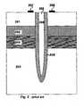
- Fig. 1 shows deep trench isolation as is currently used in the I3T50 technology of Amis (see F. De Pestel et al., "Development of a Robust 50V 0.35 ⁇ m Based Smart Power Technology Using Trench Isolation", ISPSD 2003, pp182-185 .).
- a highly doped buried layer (102) of opposite doping is created by ion implantation and subsequent thermal annealing.
- a blanket i.e. non-masked approach a sheet resistance of ⁇ 12-15 ⁇ /square can be achieved. A lower sheet resistance would require too high implantation doses, resulting in excessive defect formation.
- a low resistive buried layer is advantageous as it can serve as the drain terminal of quasi-vertical devices (hence low drain resistance), and because it also serves as the base of the (vertical) substrate PNP.
- a highly doped base yields an inefficient bipolar device, thus reducing the injection of carriers in the substrate.
- a lowly doped epitaxial layer (101) of the same conductivity type as the buried layer is grown. All active devices will be made in the lowly doped epitaxial layer.
- a self-aligned sinker (104) of the same conductivity type as the buried layer (102) is made. Two epitaxial pockets are isolated from each other by a deep trench structure (110).
- a thick isolation layer (106) is grown or deposited on the trench sidewall. This can be oxide, nitride, or a combination of both.
- the remaining trench is filled with a filling material (107) like polysilicon or oxide. Both epitaxial pockets are connected by metal contacts (108) and (109). If necessary, also the trench polyilicon (107) can be separately contacted and biased.
- a p-stop implant (105) is implanted at the trench bottom after trench etch.
- Fig. 2 shows another known arrangement, as shown in US6734524 .
- a deep trench is etched in a silicon layer stack comprising of a substrate (203) of a given conductivity type, a layer (204) of the same conductivity type but with a lower doping than (203), a layer (202) of the opposite conductivity type and finally a layer (201) of either conductivity type.
- the trench has an insulating layer (205) and is filled with a conductive material (206) for stress relief.
- the advantage of this structure is that it yields a good isolation from the substrate due to the low diffusion length of electrons (minority carriers) in the substrate.
- An object of the invention is to provide improved integrated semiconductor devices having isolation trenches, and to corresponding methods of manufacture.
- the invention provides:
- An integrated semiconductor device having a first semiconductor layer of a first conductivity type, a second semiconductor layer of the first conductivity type over the first layer, a third semiconductor layer of a second conductivity type and high doping concentration over the second layer, and an isolation trench (extending through the entire depth of the second and third layers into the first layer, characterised in that the integrated semiconductor device furthermore comprises a lowly doped first region of the second conductivity type located next to the isolation trench and extending from an interface between the second and third layers, along an interface between the second layer and the isolation trench.
- the present invention also provides a method of manufacturing an integrated semiconductor device, having the steps of forming a first semiconductor layer of a first conductivity type, forming a second semiconductor layer of the first conductivity type over the first layer, forming a third semiconductor layer of a second conductivity type and high doping concentration over the second layer, and forming an isolation trench extending through the entire depth of the second and third layers into the first layer, characterised in that the method furthermore comprises forming a lowly doped first region of the second conductivity type next to the isolation trench and extending from an interface between the second and third layers, along an interface between the second layer and the isolation trench.
- Another aspect is:
- An integrated semiconductor device having a first semiconductor layer of a first conductivity type, a second semiconductor layer of the first conductivity type over the first layer and having a lower doping level than that of the first layer, a third semiconductor layer of a second conductivity type and high doping concentration over the second layer, an isolation trench extending through the entire depth of the second and third layers into the first layer, and a lowly doped first region of the second conductivity type located next to the isolation trench and extending from an interface between the second and third layers, along an interface between the second layer and the isolation trench.
- This first region can help provide an improved reverse breakdown characteristic for the device.
- it can help reduce a concentration of field lines as shown in figs 4a and 4b , where the isolation trench meets the interface of the second and third layers, and hence provide a better reverse breakdown characteristic.
- This in turn can reduce or avoid the need for a thicker isolation trench to achieve the same purpose.
- the surface area needed can be reduced, or characteristics improved for a given surface area.
- Other aspects of the invention include methods of manufacture of such devices.
- Another aspect not being part of the present invention provides an integrated semiconductor device having a first semiconductor layer of a first conductivity type, a second semiconductor layer of the first conductivity type over the first layer, a third semiconductor layer of a second conductivity type over the second layer, an isolation trench extending through the entire depth of the second and third layers into the first layer, and having a fourth semiconductor layer of either conductivity type, over the third semiconductor layer, and having one or more active devices in the fourth layer, the isolation trench extending through the fourth layer.
- the embodiments described show examples of how to make isolation structures that account for both lateral isolation (component-to-component) as well as vertical isolation (component-to-substrate).
- the structures should be area-efficient and be able to compete with SOI with respect to the substrate isolation at high temperature. Moreover, the breakdown of the structures should be sufficiently high. Unlike SOI, the embodiments using the proposed solution can be cost-competitive and need no buried oxide, thus enabling avoiding improving the power dissipation and temperature rise due to power pulsing. At least some of the embodiments can combine the area-efficiency of trench isolation with the thermal advantageous properties of silicon compared to oxide.
- the vertical isolation is guaranteed by using a p++/p-/n++/n- type arrangement for the stack of layers. In some embodiments, the reverse breakdown is improved by a novel approach.
- the integrated semiconductor structure can have a first semiconductor layer, e.g. silicon layer of the first conductivity type, a second semiconductor layer, e.g. silicon layer of the same conductivity type and lower doping concentration, a third semiconductor layer, e.g. silicon layer of the second conductivity type and high doping concentration, and a fourth layer of either conductivity type and lower doping concentration.
- the first layer preferably has a high doping concentration, but this is not mandatory.
- the second and fourth layers have a lower doping concentration.
- a deep trench is present and extends from the silicon surface into the first silicon layer.
- a highly doped connection is made between the third layer and the semiconductor, e.g.
- the silicon surface being of the same conductivity type as the third layer, and made self-aligned to the trench.
- This extension can be made by diffusion from a solid state source, or by ion implantation.
- a lowly doped extension along the trench sidewall and in the second layer is made, being of the same conductivity type as the third layer, and also made self-aligned to the trench. This enables an increase in the reverse blocking voltage of the structure.
- the lowly doped extension can be made by diffusion from a solid state source, or by ion implantation.
- One way to make a very lowly doped buried layer is by means of an epitaxial process. In this way, no ion implantation nor thermal annealing is necessary.
- the sheet resistance of the third semiconductor, e.g. silicon layer can be decreased below 4 ⁇ /square, a value which is not achievable by conventional methods.
- One way to make the complete stack of silicon layers is to use a single epitaxial process step.
- the layers can be made from other semiconductor materials or combinations of materials to achieve similar functions.
- the making of layer (304a) can be by either ion implantation or diffusion from a solid source for example.
- layer (304b) can be by either ion implantation or by diffusion from solid source (313) for example, where the first trench (312) is suitably deep etched so that the diffused profile (304a) extends into layer (305) thus forming layer (304b).
- Another embodiment has a structure where the first semiconductor, e.g. silicon layer has the same doping as the second semiconductor, e.g. silicon layer. If the doping is high, the reverse breakdown voltage will be determined by the planar junction breakdown between layers (302) and (305) and will be low. If the doping is low, a stopper implant (105) is to be processed at the bottom of the trench prior to the formation of the insulating layer (306) to prevent MOS turn-on.
- the first semiconductor e.g. silicon layer has the same doping as the second semiconductor, e.g. silicon layer. If the doping is high, the reverse breakdown voltage will be determined by the planar junction breakdown between layers (302) and (305) and will be low. If the doping is low, a stopper implant (105) is to be processed at the bottom of the trench prior to the formation of the insulating layer (306) to prevent MOS turn-on.
- Another embodiment has a structure where layer (304b) is not extending through layer (302).
- a cut corner structure has a change in direction of less than 90° angle, hence reducing the internal electric field at the device corners.
- Fig. 3 shows an embodiment of the present invention.
- a deep trench is etched in a semiconductor, e.g. silicon layer stack comprising a substrate (303) of a given conductivity type, a layer (305) of the same conductivity type but with a lower doping than (303), a layer (302) of the opposite conductivity type and finally a layer (301) of either conductivity type.
- the buried layer 302 isolates the layer 301 from the substrate 303.
- Active devices such as transistors, diodes, switches and/or passive device such as resistors, capacitors, inductors, may be formed into layer 301.
- the doping level of the buried layer 302 may be higher than that of the layer 301. Two examples of active devices that can be formed in layer (301) can be seen on figure 3 .
- An active device can be a three-(or more)-terminal device such as a transistor.
- a first MOS transistor of the opposite conductivity type to that of layer 301 comprises a drain (314) and a source (315) e.g. diffused into layer 301, a gate 317 and a gate oxide (316).
- a second MOS transistor of the same conductivity type as that of the layer 301 can be integrated as well: a well 320 of a conductivity type opposite to that of layer 301 is formed, a drain (318) and a source (319) are then formed as well as a gate dielectric (321) and a gate electrode (322).
- the contacts to the drains 314 and 318 and to the sources 315 and 319 have not been drawn for the sake of clarity.
- Passive devices are well known and include resistors, inductors and capacitors.
- a first resistor is formed (region 323) either directly in layer 301 or in a well 324 previously formed in layer 301. Region 323 is e.g. implanted, diffused, ...The resistor is contacted through contact 325 and 326.
- a second resistor 327 is formed on top of layer 301. Layer 301 and region 327 may or may not be isolated by a dielectric 328. The resistor is contacted through contact 329 and 330.
- capacitors, diodes, inductances, ... can be formed in layer 301 and/or above layer 301.
- Doping concentration of layer (303) is typically in the 10 18 -10 19 cm -3 range. Thickness and doping of layer (305) depends on the blocking voltage requirement but is typically around 10 15 -10 16 cm -3 with thickness between 25 and 5 ⁇ m for blocking voltages between 250V and 10V.
- Layer (302) preferably has a very low sheet resistance, hence has a very high doping concentration, typically in the 10 19 cm -3 range. This can be achieved by ion implantation with doses in the low 10 16 cm -2 range.
- a typical concentration range for layer (301) is between 10 15 and 10 17 cm -3 for devices with a blocking capability between 250V and 10V.
- the thickness of layer (301) is typically between 2 and 12 ⁇ m.
- the trench has an insulating layer (306) and is filled with a conductive material (307) for stress relief.
- Layer (306) should be suitably thick in order to withstand a high field across it.
- the oxide thickness is typically between 500 and 1000 nm.
- a highly doped region (304a) is formed at the top of the trenches to contact the layer (302).
- This second region (304a) can have a very low sheet resistance, by using a high doping concentration (range 10 18 -10 19 cm -3 ). In this way, a self-aligned and area-effective way is found for contacting layer (302) at the top of the semiconductor, e.g. silicon.
- Second region (304a) has the same conductivity type as layer (302).
- a lightly doped layer (304b) is formed underneath layer (302) and into layer (305).
- First region (304b) has the same conductivity type as layer (302), but the opposite conductivity type of layer (305).
- a junction is formed in layer (305), adjacent to the trench sidewall (306). This extra junction will be depleted upon reverse biasing of the structure, thus supporting part of the voltage drop and relaxing the potential drop and crowding over the liner oxide. As a result, the reverse blocking voltage of the structure will be substantially increased.
- the concentration of region (304b) is in the 10 16 cm -3 range but needs to be optimized for a given breakdown voltage and layer (305) concentration. As an example. for V bd in excess of 100V, the optimum concentration is 2.10 16 cm -3 when the concentration of layer (305) is 10 15 cm -3 . See also Fig. 4d .
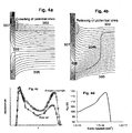
- Figs. 4a to 4d show graphs relating to an explanation of device operation according to an embodiment of the present invention.
- Fig. 4a shows for reference the problems that can arise when a structure without region 304b is reverse biased.
- the trench inner poly 310 will be at a given potential, be it externally biased or be it floating.
- the potential of the inner polysilicon layer will be determined by the potential at the different contacts and of the substrate, as well as the part of the trench in each pocket i.e. its total capacitance.
- the voltage in the trench is then determined by a capacitive divider.
- the polysilicon of the trench is suitably doped, it will act as an equipotential plane.
- the potential lines in the semiconductor e.g. silicon will be concentrated where they bend at the trench liner oxide near the interface between layers 302 and 305.
- Fig. 4b shows the effect of implementing a suitably doped region (304b) adjacent to the trench and into layer (305), and of the opposite conductivity type, thus creating a p-n junction in layer (305). Due to the presence of this extra junction, the potential lines are smoothed, and are more relaxed, as is seen in Fig. 4b.
- Fig. 4c shows the electric field profile along a cross-section parallel to the trench interface, clearly revealing two distinct peaks (potential lines are less bent at the top, but more bent at the bottom of the structure). Thus the reverse blocking voltage (being the integral of the electric field profile) is increased compared to the reference example of fig 4a.
- Fig. 4d shows that the breakdown voltage is dependent on the doping of the first region (304b).
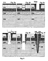
- Figs 5a to 5f show steps in a method of manufacturing according to an embodiment of the present invention having the distinctive four layer structure and the distinctive first and second regions.
- Fig. 5a One starts with a semiconductor, e.g. silicon substrate of a given conductivity type (303), preferably but not necessarily with a high doping concentration (in excess of 10 18 cm-3). A layer of the same conductivity type (305) but with a lower concentration ( ⁇ 10 15 -10 16 cm -3 ) is grown on top of the first layer. Then a highly doped layer of the opposite conductivity type (302) is made. This layer can be implanted and subsequently annealed, can be deposited and annealed, or can be grown in an epitaxial reactor. The doping concentration should be in excess of 10 18 cm -3 . Then another layer (301) of either conductivity type but with a lower doping concentration, is grown.
- a semiconductor e.g. silicon substrate of a given conductivity type (303), preferably but not necessarily with a high doping concentration (in excess of 10 18 cm-3).
- all layers (305)-(302)-(301) are grown in an epitaxial-reactor, yielding the possibility to make a very low resistive layer (302) (rho sheet less than 5 ⁇ /square).
- a very low resistive layer (302) (rho sheet less than 5 ⁇ /square).
- the implantation and annealing steps are skipped in the process flow.
- such a low resistive layer cannot be made by implantation due to crystal defects.
- layer (302) would be made by diffusion from a solid source, the diffusion tail will be large thus requiring the need to increase the thickness of layer (305) and the total trench depth.
- a hard mask (311) is deposited.
- a first trench (312) is etched into semiconductor, e.g. silicon layers (301) and (302).
- the dopants are diffused into layers (301) and (302), establishing a second region (304a), yielding a low resistive connection of layer (302) to the top of the semiconductor, e.g. silicon layer.
- the second region (304a) can also be formed by ion implantation.
- Fig. 5d, 5e With the same hardmask (311), the trench (312) is etched deeper, into layer (305) and if necessary into layer (303). An ion implantation, indicated with arrows 400, with suitable angle and dose is performed, as to make the first region of the second conductivity type (304b). The doping of region (304b) can eventually also be carried out by diffusion from a suitably doped solid state source. The trench (312) can extend into layer (303), as the latter is highly doped and the small counterdoping of region (304b) is not expected to be significant. Then the hardmask (311) is removed.
- Fig. 5f An isolating layer (306) is grown or deposited on the trench sidewall. The thickness of the insulating layer should be sufficient to withstand a high voltage. The trench can then be filled with a stress relief material such as amorphous Silicon for stress relief, or with an insulating material. Finally, the different pockets will be contacted (contacts (308), (309)), and if desired also the trench amorphous silicon layer can be contacted (310).
- a stress relief material such as amorphous Silicon for stress relief
- inventions can include mixed analogue/digital ASIC's used in automotive, peripheral and consumer applications.
- the devices can use 0.35 ⁇ m based integrated device manufacturing technology, with device gate density of 500 kgates for example.
- the deep trench isolation for high voltage isolation means the isolation distance between the high voltage devices can be considerably reduced and hence reduce the total chip area drastically compared to technologies with a standard junction isolation scheme.
- a typical supply voltage for such devices is 36 V, for some applications a charge pump (additional 3.6 V) for external drivers can be used.
- Applications can include any smart power products, especially high temperature products.
- any type of technology can be used for the integrated circuit, examples include CMOS, bipolar or BiCMOS semiconductor devices. They can be formed in the semiconductor substrate such that the active devices are either circumscribed by the isolation trench, or a buried horizontal insulator layer can be used, so the active devices are completely surrounded by the isolation trench and the intersecting buried horizontal insulator layer.
Landscapes
- Element Separation (AREA)
Claims (19)
- Integrierte Halbleitervorrichtung mit einer ersten Halbleiterschicht (303) eines ersten Leitfähigkeitstyps, einer zweiten Halbleiterschicht (305) des ersten Leitfähigkeitstyps über der ersten Schicht, einer dritten Halbleiterschicht (302) eines zweiten Leitfähigkeitstyps und mit hoher Dotierungskonzentration über der zweiten Schicht und einem Isolationsgraben (307), der sich durch die gesamte Tiefe der zweiten und dritten Schicht in die erste Schicht erstreckt,
dadurch gekennzeichnet, dass die integrierte Halbleitervorrichtung des Weiteren eine nieder dotierte erste Region (304b) des zweiten Leitfähigkeitstyps umfasst, die nahe dem Isolationsgraben angeordnet ist und sich von einer Grenzfläche zwischen der zweiten und dritten Schicht, entlang einer Grenzfläche zwischen der zweiten Schicht und dem Isolationsgraben erstreckt. - Vorrichtung nach Anspruch 1 mit einer vierten Halbleiterschicht (301) eines beliebigen Leitfähigkeitstyps über der dritten Halbleiterschicht und mit einer oder mehreren aktiven Vorrichtungen in der vierten Schicht, wobei sich der Isolationsgraben durch die vierte Schicht erstreckt.
- Vorrichtung nach Anspruch 2 mit einer zweiten Region (304a) des zweiten Leitfähigkeitstyps, die sich nahe dem Isolationsgraben befindet und durch die vierte schicht in Kontakt mit der dritten Halbleiterschicht erstreckt.
- Vorrichtung nach Anspruch 3, wobei sich die zweite Region (304a) nicht durch die dritte Schicht (302) erstreckt.
- Vorrichtung nach einem der vorangehenden Ansprüche, wobei ein Flächenwiderstand der dritten Siliziumschicht unter 4Ω/Quadrat ist.
- Vorrichtung nach Anspruch 2 oder einem Anspruch abhängig von Anspruch 2, wobei die erste, zweite, dritte und vierte Halbleiterschicht die Form eines Stapels von Siliziumschichten mit p++/p-/n++/n- Typen aufweisen.
- Vorrichtung nach einem der vorangehenden Ansprüche, wobei die erste Halbleiterschicht einen höheren Dotierungswert aufweist als die zweite Schicht.
- Vorrichtung nach einem der vorangehenden Ansprüche, wobei die erste Halbleiterschicht denselben Dotierungswert wie die zweite Siliziumschicht hat.
- Vorrichtung nach einem der vorangehenden Ansprüche mit einem Anschlag (105) am Boden des Isolationsgrabens.
- Vorrichtung nach einem der vorangehenden Ansprüche mit einer oder mehr Ecken in einem Pfad des Grabens entlang einer Ebene der Schichten, wobei die Ecken eine Änderung in der Richtung von kleiner oder gleich 90 Grad beinhalten.
- Verfahren zur Herstellung einer integrierten Halbleitervorrichtung mit den Schritten des Bildens einer ersten Halbleiterschicht (303) eines ersten Leitfähigkeitstyps, des Bildens einer zweiten Halbleiterschicht (305) des ersten Leitfähigkeitstyps über der ersten Schicht, des Bildens einer dritten Halbleiterschicht (302) eines zweiten Leitfähigkeitstyps und mit hoher Dotierungskonzentration über der zweiten Schicht und des Bildens eines Isolationsgrabens (307), der sich durch die gesamte Tiefe der zweiten und dritten Schicht in die erste Schicht erstreckt,
dadurch gekennzeichnet, dass das Verfahren des Weiteren das Bilden einer nieder dotierten ersten Region (304b) des zweiten Leitfähigkeitstyps nahe dem Isolationsgraben umfasst, die sich von einer Grenzfläche zwischen der zweiten und dritten Schicht, entlang einer Grenzfläche zwischen der zweiten Schicht und dem Isolationsgraben erstreckt. - Verfahren nach Anspruch 11, mit den Schritten des Bildens einer vierten Halbleiterschicht (301) eines beliebigen Leitfähigkeitstyps über der dritten Schicht vor der Bildung des Isolationsgrabens, wobei der Isolationsgraben so gebildet ist, dass er sich durch die vierte Schicht erstreckt, und des Bildens einer oder mehrerer aktiver Vorrichtungen in der vierten Schicht.
- Verfahren nach Anspruch 11 oder 12, mit dem Schritt des Bildens einer zweiten Region (304a) des zweiten Leitfähigkeitstyps in Selbstausrichtung zu dem Isolationsgraben, die sich durch die vierte Schicht in Kontakt mit der dritten Schicht erstreckt.
- Verfahren nach Anspruch 13, wobei der Schritt des Bildens der zweiten Region das Implantieren oder Diffundieren eines gewählten Teils einer Seitenwand des Grabens vor dem Füllen des Grabens umfasst.
- Verfahren nach einem der Ansprüche 11 bis 14, wobei der Schritt des Bildens der ersten Region das Implantieren oder Diffundieren eines gewählten Teils einer Seitenwand des Grabens vor dem Füllen des Grabens umfasst.
- Verfahren nach einem der Ansprüche 11 bis 15 mit dem Schritt des Bildens der dritten Schicht durch einen Epitaxialprozess.
- Verfahren nach einem der Ansprüche 12 bis 16 mit dem Schritt des Bildens der ersten, zweiten, dritten und vierten Halbleiterschichten in der Form eines Stapels von Siliziumschichten unter Verwendung eines einzigen epitaxialen Verfahrensschrittes.
- Verfahren nach einem der Ansprüche 12 bis 17, wobei der Schritt zum Bilden des Isolationsgrabens einen Schritt des Bildens eines ersten Grabens (312) durch die vierte Schicht zu der dritten Schicht, des Ausführens eines Verfahrensschrittes und anschließend des Vertiefens des Grabens durch die dritte und zweite Schicht zu der ersten Schicht umfasst.
- Verfahren nach Anspruch 18 mit dem weiteren Schritt des Bildens der ersten und zweiten Region, bevor der Graben ein zweites Mal vertieft wird.
Priority Applications (4)
| Application Number | Priority Date | Filing Date | Title |
|---|---|---|---|
| AT07012746T ATE458274T1 (de) | 2007-06-29 | 2007-06-29 | Tiefgrabenisolationsstrukturen in integrierten halbleiterbauelementen |
| DE602007004839T DE602007004839D1 (de) | 2007-06-29 | 2007-06-29 | Tiefgrabenisolationsstrukturen in integrierten Halbleiterbauelementen |
| EP07012746A EP2009686B1 (de) | 2007-06-29 | 2007-06-29 | Tiefgrabenisolationsstrukturen in integrierten Halbleiterbauelementen |
| US12/163,909 US8115273B2 (en) | 2007-06-29 | 2008-06-27 | Deep trench isolation structures in integrated semiconductor devices |
Applications Claiming Priority (1)
| Application Number | Priority Date | Filing Date | Title |
|---|---|---|---|
| EP07012746A EP2009686B1 (de) | 2007-06-29 | 2007-06-29 | Tiefgrabenisolationsstrukturen in integrierten Halbleiterbauelementen |
Publications (2)
| Publication Number | Publication Date |
|---|---|
| EP2009686A1 EP2009686A1 (de) | 2008-12-31 |
| EP2009686B1 true EP2009686B1 (de) | 2010-02-17 |
Family
ID=38604852
Family Applications (1)
| Application Number | Title | Priority Date | Filing Date |
|---|---|---|---|
| EP07012746A Not-in-force EP2009686B1 (de) | 2007-06-29 | 2007-06-29 | Tiefgrabenisolationsstrukturen in integrierten Halbleiterbauelementen |
Country Status (4)
| Country | Link |
|---|---|
| US (1) | US8115273B2 (de) |
| EP (1) | EP2009686B1 (de) |
| AT (1) | ATE458274T1 (de) |
| DE (1) | DE602007004839D1 (de) |
Families Citing this family (8)
| Publication number | Priority date | Publication date | Assignee | Title |
|---|---|---|---|---|
| JP2007129085A (ja) * | 2005-11-04 | 2007-05-24 | Texas Instr Japan Ltd | 半導体装置及びその製造方法 |
| JP5010660B2 (ja) * | 2009-09-25 | 2012-08-29 | 株式会社東芝 | 半導体装置およびその製造方法 |
| US8673723B1 (en) | 2013-02-07 | 2014-03-18 | Globalfoundries Inc. | Methods of forming isolation regions for FinFET semiconductor devices |
| US9696736B2 (en) | 2013-03-15 | 2017-07-04 | Fairchild Semiconductor Corporation | Two-terminal current limiter and apparatus thereof |
| US9679890B2 (en) * | 2013-08-09 | 2017-06-13 | Fairchild Semiconductor Corporation | Junction-less insulated gate current limiter device |
| US9735147B2 (en) | 2014-09-15 | 2017-08-15 | Fairchild Semiconductor Corporation | Fast and stable ultra low drop-out (LDO) voltage clamp device |
| US20170373142A1 (en) * | 2016-06-23 | 2017-12-28 | Littelfuse, Inc. | Semiconductor device having side-diffused trench plug |
| US10607880B2 (en) * | 2018-08-30 | 2020-03-31 | Nxp Usa, Inc. | Die with buried doped isolation region |
Family Cites Families (4)
| Publication number | Priority date | Publication date | Assignee | Title |
|---|---|---|---|---|
| US4534826A (en) * | 1983-12-29 | 1985-08-13 | Ibm Corporation | Trench etch process for dielectric isolation |
| JP3360970B2 (ja) * | 1995-05-22 | 2003-01-07 | 株式会社東芝 | 半導体装置の製造方法 |
| US6734524B1 (en) * | 2002-12-31 | 2004-05-11 | Motorola, Inc. | Electronic component and method of manufacturing same |
| US7491618B2 (en) * | 2006-01-26 | 2009-02-17 | International Business Machines Corporation | Methods and semiconductor structures for latch-up suppression using a conductive region |
-
2007
- 2007-06-29 AT AT07012746T patent/ATE458274T1/de not_active IP Right Cessation
- 2007-06-29 DE DE602007004839T patent/DE602007004839D1/de active Active
- 2007-06-29 EP EP07012746A patent/EP2009686B1/de not_active Not-in-force
-
2008
- 2008-06-27 US US12/163,909 patent/US8115273B2/en active Active
Also Published As
| Publication number | Publication date |
|---|---|
| DE602007004839D1 (de) | 2010-04-01 |
| US8115273B2 (en) | 2012-02-14 |
| US20090039460A1 (en) | 2009-02-12 |
| ATE458274T1 (de) | 2010-03-15 |
| EP2009686A1 (de) | 2008-12-31 |
Similar Documents
| Publication | Publication Date | Title |
|---|---|---|
| US10818516B2 (en) | Semiconductor device having biasing structure for self-isolating buried layer and method therefor | |
| JP5273394B2 (ja) | 垂直方向過渡電圧サプレッサ(tvs)とemiフィルタのための回路構成と製造処理 | |
| KR101900843B1 (ko) | 감소된 온-저항을 가지는 트렌치 전력 mosfet | |
| US6902967B2 (en) | Integrated circuit with a MOS structure having reduced parasitic bipolar transistor action | |
| EP2009686B1 (de) | Tiefgrabenisolationsstrukturen in integrierten Halbleiterbauelementen | |
| US11521961B2 (en) | Back ballasted vertical NPN transistor | |
| WO2019060419A1 (en) | WELLBORNE COLLECTOR CONNECTION REGION FOR NARROW DEEPENERS | |
| CN101203960B (zh) | 具有高击穿电压的半导体器件及其制造方法 | |
| KR20020059244A (ko) | 향상된 안전 동작 영역을 가진 ldmos | |
| US20040018705A1 (en) | Semiconductor structure and method for processing such a structure | |
| EP3961722A1 (de) | Vorrichtung zur erweiterung der betriebsspannung | |
| US8211766B2 (en) | Method of fabricating a trench power MOS transistor | |
| US20070246790A1 (en) | Transistor process using a double-epitaxial layer for reduced capacitance | |
| US9653459B2 (en) | MOSFET having source region formed in a double wells region | |
| CN110416208B (zh) | 电路、电子器件及其形成方法 | |
| US11289570B2 (en) | Semiconductor device having optimized drain termination and method therefor | |
| US7973360B2 (en) | Depletable cathode low charge storage diode | |
| CN120836201A (zh) | 具有自对准沟槽屏蔽区的栅极沟槽功率半导体器件及相关方法 | |
| KR100563162B1 (ko) | 반도체장치및그제조방법 | |
| KR100482950B1 (ko) | 반도체소자 및 그 제조방법 | |
| HK1127669A (en) | Deep trench isolation structures in integrated semiconductor devices | |
| CN118693144B (zh) | 半导体器件 | |
| EP4481821A1 (de) | Halbleiterchip mit vertikaler transistorvorrichtung | |
| HK1127867B (en) | Deep trench isolation for power semiconductors |
Legal Events
| Date | Code | Title | Description |
|---|---|---|---|
| PUAI | Public reference made under article 153(3) epc to a published international application that has entered the european phase |
Free format text: ORIGINAL CODE: 0009012 |
|
| 17P | Request for examination filed |
Effective date: 20081030 |
|
| AK | Designated contracting states |
Kind code of ref document: A1 Designated state(s): AT BE BG CH CY CZ DE DK EE ES FI FR GB GR HU IE IS IT LI LT LU LV MC MT NL PL PT RO SE SI SK TR |
|
| AX | Request for extension of the european patent |
Extension state: AL BA HR MK RS |
|
| 17Q | First examination report despatched |
Effective date: 20090219 |
|
| GRAP | Despatch of communication of intention to grant a patent |
Free format text: ORIGINAL CODE: EPIDOSNIGR1 |
|
| AKX | Designation fees paid |
Designated state(s): AT BE BG CH CY CZ DE DK EE ES FI FR GB GR HU IE IS IT LI LT LU LV MC MT NL PL PT RO SE SI SK TR |
|
| RIC1 | Information provided on ipc code assigned before grant |
Ipc: H01L 21/761 20060101ALI20090807BHEP Ipc: H01L 21/763 20060101ALI20090807BHEP Ipc: H01L 21/762 20060101AFI20090807BHEP |
|
| REG | Reference to a national code |
Ref country code: HK Ref legal event code: DE Ref document number: 1127669 Country of ref document: HK |
|
| RAP1 | Party data changed (applicant data changed or rights of an application transferred) |
Owner name: SEMICONDUCTOR COMPONENTS INDUSTRIES, LLC |
|
| GRAS | Grant fee paid |
Free format text: ORIGINAL CODE: EPIDOSNIGR3 |
|
| GRAA | (expected) grant |
Free format text: ORIGINAL CODE: 0009210 |
|
| AK | Designated contracting states |
Kind code of ref document: B1 Designated state(s): AT BE BG CH CY CZ DE DK EE ES FI FR GB GR HU IE IS IT LI LT LU LV MC MT NL PL PT RO SE SI SK TR |
|
| REG | Reference to a national code |
Ref country code: GB Ref legal event code: FG4D |
|
| REG | Reference to a national code |
Ref country code: CH Ref legal event code: EP |
|
| REG | Reference to a national code |
Ref country code: IE Ref legal event code: FG4D |
|
| REF | Corresponds to: |
Ref document number: 602007004839 Country of ref document: DE Date of ref document: 20100401 Kind code of ref document: P |
|
| RIN2 | Information on inventor provided after grant (corrected) |
Inventor name: BAELE, JORIS Inventor name: MOENS, PETER Inventor name: BAUWENS, FILIP |
|
| REG | Reference to a national code |
Ref country code: NL Ref legal event code: VDEP Effective date: 20100217 |
|
| LTIE | Lt: invalidation of european patent or patent extension |
Effective date: 20100217 |
|
| PG25 | Lapsed in a contracting state [announced via postgrant information from national office to epo] |
Ref country code: IS Free format text: LAPSE BECAUSE OF FAILURE TO SUBMIT A TRANSLATION OF THE DESCRIPTION OR TO PAY THE FEE WITHIN THE PRESCRIBED TIME-LIMIT Effective date: 20100617 Ref country code: PT Free format text: LAPSE BECAUSE OF FAILURE TO SUBMIT A TRANSLATION OF THE DESCRIPTION OR TO PAY THE FEE WITHIN THE PRESCRIBED TIME-LIMIT Effective date: 20100617 Ref country code: ES Free format text: LAPSE BECAUSE OF FAILURE TO SUBMIT A TRANSLATION OF THE DESCRIPTION OR TO PAY THE FEE WITHIN THE PRESCRIBED TIME-LIMIT Effective date: 20100528 Ref country code: LT Free format text: LAPSE BECAUSE OF FAILURE TO SUBMIT A TRANSLATION OF THE DESCRIPTION OR TO PAY THE FEE WITHIN THE PRESCRIBED TIME-LIMIT Effective date: 20100217 |
|
| PG25 | Lapsed in a contracting state [announced via postgrant information from national office to epo] |
Ref country code: SI Free format text: LAPSE BECAUSE OF FAILURE TO SUBMIT A TRANSLATION OF THE DESCRIPTION OR TO PAY THE FEE WITHIN THE PRESCRIBED TIME-LIMIT Effective date: 20100217 Ref country code: AT Free format text: LAPSE BECAUSE OF FAILURE TO SUBMIT A TRANSLATION OF THE DESCRIPTION OR TO PAY THE FEE WITHIN THE PRESCRIBED TIME-LIMIT Effective date: 20100217 Ref country code: FI Free format text: LAPSE BECAUSE OF FAILURE TO SUBMIT A TRANSLATION OF THE DESCRIPTION OR TO PAY THE FEE WITHIN THE PRESCRIBED TIME-LIMIT Effective date: 20100217 Ref country code: LV Free format text: LAPSE BECAUSE OF FAILURE TO SUBMIT A TRANSLATION OF THE DESCRIPTION OR TO PAY THE FEE WITHIN THE PRESCRIBED TIME-LIMIT Effective date: 20100217 Ref country code: PL Free format text: LAPSE BECAUSE OF FAILURE TO SUBMIT A TRANSLATION OF THE DESCRIPTION OR TO PAY THE FEE WITHIN THE PRESCRIBED TIME-LIMIT Effective date: 20100217 |
|
| PG25 | Lapsed in a contracting state [announced via postgrant information from national office to epo] |
Ref country code: EE Free format text: LAPSE BECAUSE OF FAILURE TO SUBMIT A TRANSLATION OF THE DESCRIPTION OR TO PAY THE FEE WITHIN THE PRESCRIBED TIME-LIMIT Effective date: 20100217 Ref country code: BE Free format text: LAPSE BECAUSE OF FAILURE TO SUBMIT A TRANSLATION OF THE DESCRIPTION OR TO PAY THE FEE WITHIN THE PRESCRIBED TIME-LIMIT Effective date: 20100217 Ref country code: CY Free format text: LAPSE BECAUSE OF FAILURE TO SUBMIT A TRANSLATION OF THE DESCRIPTION OR TO PAY THE FEE WITHIN THE PRESCRIBED TIME-LIMIT Effective date: 20100217 Ref country code: SE Free format text: LAPSE BECAUSE OF FAILURE TO SUBMIT A TRANSLATION OF THE DESCRIPTION OR TO PAY THE FEE WITHIN THE PRESCRIBED TIME-LIMIT Effective date: 20100217 Ref country code: RO Free format text: LAPSE BECAUSE OF FAILURE TO SUBMIT A TRANSLATION OF THE DESCRIPTION OR TO PAY THE FEE WITHIN THE PRESCRIBED TIME-LIMIT Effective date: 20100217 Ref country code: GR Free format text: LAPSE BECAUSE OF FAILURE TO SUBMIT A TRANSLATION OF THE DESCRIPTION OR TO PAY THE FEE WITHIN THE PRESCRIBED TIME-LIMIT Effective date: 20100518 Ref country code: NL Free format text: LAPSE BECAUSE OF FAILURE TO SUBMIT A TRANSLATION OF THE DESCRIPTION OR TO PAY THE FEE WITHIN THE PRESCRIBED TIME-LIMIT Effective date: 20100217 |
|
| PG25 | Lapsed in a contracting state [announced via postgrant information from national office to epo] |
Ref country code: CZ Free format text: LAPSE BECAUSE OF FAILURE TO SUBMIT A TRANSLATION OF THE DESCRIPTION OR TO PAY THE FEE WITHIN THE PRESCRIBED TIME-LIMIT Effective date: 20100217 Ref country code: SK Free format text: LAPSE BECAUSE OF FAILURE TO SUBMIT A TRANSLATION OF THE DESCRIPTION OR TO PAY THE FEE WITHIN THE PRESCRIBED TIME-LIMIT Effective date: 20100217 Ref country code: BG Free format text: LAPSE BECAUSE OF FAILURE TO SUBMIT A TRANSLATION OF THE DESCRIPTION OR TO PAY THE FEE WITHIN THE PRESCRIBED TIME-LIMIT Effective date: 20100517 |
|
| PLBE | No opposition filed within time limit |
Free format text: ORIGINAL CODE: 0009261 |
|
| STAA | Information on the status of an ep patent application or granted ep patent |
Free format text: STATUS: NO OPPOSITION FILED WITHIN TIME LIMIT |
|
| 26N | No opposition filed |
Effective date: 20101118 |
|
| PG25 | Lapsed in a contracting state [announced via postgrant information from national office to epo] |
Ref country code: MC Free format text: LAPSE BECAUSE OF NON-PAYMENT OF DUE FEES Effective date: 20100630 Ref country code: DK Free format text: LAPSE BECAUSE OF FAILURE TO SUBMIT A TRANSLATION OF THE DESCRIPTION OR TO PAY THE FEE WITHIN THE PRESCRIBED TIME-LIMIT Effective date: 20100217 |
|
| PG25 | Lapsed in a contracting state [announced via postgrant information from national office to epo] |
Ref country code: IT Free format text: LAPSE BECAUSE OF NON-PAYMENT OF DUE FEES Effective date: 20100629 |
|
| PG25 | Lapsed in a contracting state [announced via postgrant information from national office to epo] |
Ref country code: MT Free format text: LAPSE BECAUSE OF FAILURE TO SUBMIT A TRANSLATION OF THE DESCRIPTION OR TO PAY THE FEE WITHIN THE PRESCRIBED TIME-LIMIT Effective date: 20100217 Ref country code: IE Free format text: LAPSE BECAUSE OF NON-PAYMENT OF DUE FEES Effective date: 20100629 |
|
| REG | Reference to a national code |
Ref country code: CH Ref legal event code: PL |
|
| GBPC | Gb: european patent ceased through non-payment of renewal fee |
Effective date: 20110629 |
|
| PG25 | Lapsed in a contracting state [announced via postgrant information from national office to epo] |
Ref country code: CH Free format text: LAPSE BECAUSE OF NON-PAYMENT OF DUE FEES Effective date: 20110630 Ref country code: LI Free format text: LAPSE BECAUSE OF NON-PAYMENT OF DUE FEES Effective date: 20110630 |
|
| PG25 | Lapsed in a contracting state [announced via postgrant information from national office to epo] |
Ref country code: GB Free format text: LAPSE BECAUSE OF NON-PAYMENT OF DUE FEES Effective date: 20110629 |
|
| PGFP | Annual fee paid to national office [announced via postgrant information from national office to epo] |
Ref country code: FR Payment date: 20120614 Year of fee payment: 6 |
|
| PG25 | Lapsed in a contracting state [announced via postgrant information from national office to epo] |
Ref country code: LU Free format text: LAPSE BECAUSE OF NON-PAYMENT OF DUE FEES Effective date: 20100629 Ref country code: HU Free format text: LAPSE BECAUSE OF FAILURE TO SUBMIT A TRANSLATION OF THE DESCRIPTION OR TO PAY THE FEE WITHIN THE PRESCRIBED TIME-LIMIT Effective date: 20100818 |
|
| PGFP | Annual fee paid to national office [announced via postgrant information from national office to epo] |
Ref country code: IT Payment date: 20120618 Year of fee payment: 6 |
|
| PG25 | Lapsed in a contracting state [announced via postgrant information from national office to epo] |
Ref country code: TR Free format text: LAPSE BECAUSE OF FAILURE TO SUBMIT A TRANSLATION OF THE DESCRIPTION OR TO PAY THE FEE WITHIN THE PRESCRIBED TIME-LIMIT Effective date: 20100217 |
|
| REG | Reference to a national code |
Ref country code: FR Ref legal event code: ST Effective date: 20140228 |
|
| PG25 | Lapsed in a contracting state [announced via postgrant information from national office to epo] |
Ref country code: IT Free format text: LAPSE BECAUSE OF NON-PAYMENT OF DUE FEES Effective date: 20130629 Ref country code: FR Free format text: LAPSE BECAUSE OF NON-PAYMENT OF DUE FEES Effective date: 20130701 |
|
| REG | Reference to a national code |
Ref country code: HK Ref legal event code: WD Ref document number: 1127669 Country of ref document: HK |
|
| PGFP | Annual fee paid to national office [announced via postgrant information from national office to epo] |
Ref country code: DE Payment date: 20200519 Year of fee payment: 14 |
|
| REG | Reference to a national code |
Ref country code: DE Ref legal event code: R119 Ref document number: 602007004839 Country of ref document: DE |
|
| PG25 | Lapsed in a contracting state [announced via postgrant information from national office to epo] |
Ref country code: DE Free format text: LAPSE BECAUSE OF NON-PAYMENT OF DUE FEES Effective date: 20220101 |