EP2009683A2 - Zinkoxidhalbleiter und Verfahren zu seiner Herstellung - Google Patents
Zinkoxidhalbleiter und Verfahren zu seiner Herstellung Download PDFInfo
- Publication number
- EP2009683A2 EP2009683A2 EP08104509A EP08104509A EP2009683A2 EP 2009683 A2 EP2009683 A2 EP 2009683A2 EP 08104509 A EP08104509 A EP 08104509A EP 08104509 A EP08104509 A EP 08104509A EP 2009683 A2 EP2009683 A2 EP 2009683A2
- Authority
- EP
- European Patent Office
- Prior art keywords
- zinc oxide
- thin film
- oxide thin
- heat treatment
- metal catalyst
- Prior art date
- Legal status (The legal status is an assumption and is not a legal conclusion. Google has not performed a legal analysis and makes no representation as to the accuracy of the status listed.)
- Withdrawn
Links
Images
Classifications
-
- H—ELECTRICITY
- H10—SEMICONDUCTOR DEVICES; ELECTRIC SOLID-STATE DEVICES NOT OTHERWISE PROVIDED FOR
- H10P—GENERIC PROCESSES OR APPARATUS FOR THE MANUFACTURE OR TREATMENT OF DEVICES COVERED BY CLASS H10
- H10P14/00—Formation of materials, e.g. in the shape of layers or pillars
- H10P14/20—Formation of materials, e.g. in the shape of layers or pillars of semiconductor materials
- H10P14/38—Formation of materials, e.g. in the shape of layers or pillars of semiconductor materials characterised by treatments done after the formation of the materials
- H10P14/3802—Crystallisation or recrystallisation of non-monocrystalline semiconductor materials, e.g. regrowth
-
- H—ELECTRICITY
- H10—SEMICONDUCTOR DEVICES; ELECTRIC SOLID-STATE DEVICES NOT OTHERWISE PROVIDED FOR
- H10P—GENERIC PROCESSES OR APPARATUS FOR THE MANUFACTURE OR TREATMENT OF DEVICES COVERED BY CLASS H10
- H10P14/00—Formation of materials, e.g. in the shape of layers or pillars
- H10P14/20—Formation of materials, e.g. in the shape of layers or pillars of semiconductor materials
- H10P14/29—Formation of materials, e.g. in the shape of layers or pillars of semiconductor materials characterised by the substrates
- H10P14/2901—Materials
-
- H—ELECTRICITY
- H10—SEMICONDUCTOR DEVICES; ELECTRIC SOLID-STATE DEVICES NOT OTHERWISE PROVIDED FOR
- H10P—GENERIC PROCESSES OR APPARATUS FOR THE MANUFACTURE OR TREATMENT OF DEVICES COVERED BY CLASS H10
- H10P14/00—Formation of materials, e.g. in the shape of layers or pillars
- H10P14/20—Formation of materials, e.g. in the shape of layers or pillars of semiconductor materials
- H10P14/34—Deposited materials, e.g. layers
- H10P14/3402—Deposited materials, e.g. layers characterised by the chemical composition
- H10P14/3424—Deposited materials, e.g. layers characterised by the chemical composition being Group IIB-VIA materials
- H10P14/3426—Oxides
-
- H—ELECTRICITY
- H10—SEMICONDUCTOR DEVICES; ELECTRIC SOLID-STATE DEVICES NOT OTHERWISE PROVIDED FOR
- H10P—GENERIC PROCESSES OR APPARATUS FOR THE MANUFACTURE OR TREATMENT OF DEVICES COVERED BY CLASS H10
- H10P14/00—Formation of materials, e.g. in the shape of layers or pillars
- H10P14/20—Formation of materials, e.g. in the shape of layers or pillars of semiconductor materials
- H10P14/34—Deposited materials, e.g. layers
- H10P14/3438—Doping during depositing
- H10P14/3441—Conductivity type
- H10P14/3444—P-type
Definitions
- the present invention relates to a zinc oxide semiconductor, and more particularly, to a method of manufacturing a p-type zinc oxide semiconductor and a p-type zinc oxide semiconductor manufactured using the method.
- a zinc oxide semiconductor is a group II-VI semiconductor, and has the hexagonal wurzite structure.
- the zinc oxide semiconductor has the structure similar to the structure of a GaN-based material that is currently used in a light emitting device, and many researches have been performed on the zinc oxide semiconductor as a light source at home and abroad.
- a zinc oxide semiconductor has an optical band gap of 3.37 eV at a normal temperature, and may be used as a light source in a near ultraviolet region, which makes it possible to allow a blue light emitting device to be used as a light source using a white light emitting diode.
- an exciton bonding energy of the zinc oxide semiconductor at the normal temperature is larger than that of GaN at the normal temperature. Therefore, when the zinc oxide semiconductor is used in a field of a photoelectric device using an exciton, it is possible to expect a high optical gain.
- the zinc oxide semiconductor since having excellent conductivity and transparency, the zinc oxide semiconductor has been applied to various photoelectric devices, such as a transparent electrode, a sound acoustic wave device, and a varistor device.
- the zinc oxide semiconductor is not evaporated stoichiometrically in an actual process for forming a thin film, and has the characteristic of an n-type semiconductor due to the surplus of zinc or the lack of oxygen.
- the research on the manufacture of an n-type zinc oxide semiconductor has been developed heretofore, but the manufacture of a p-type zinc oxide semiconductor essential for a photoelectric device or a photoelectric device is not completely successful.
- a photoelectric device emits light corresponding to an energy generated while a hole and an electron are necessarily combined with each other. Further, since a channel is formed of a hole in the case of a p-type thin film transistor, a good p-type thin film transistor should be manufactured in order to manufacture the above-mentioned electronic devices.
- the reason why the p-type zinc oxide semiconductor thin film is difficult to be manufactured is that the solubility of group I and V elements for forming holes is very low in the zinc oxide. Further, hydrogen adulterated during the growth of the thin film forms a dopant-H(hydrogen) or O (oxygen)-H(hydrogen) complex body, and provides electrons into the thin film, so that holes are compensated. Therefore, there is a problem in that it is difficult to form holes in the thin film [ C. G. Van de Walle et al, Nature 423, 626(2003 )].
- Japanese Yamamoto group [ T. Yamamoto et al, Jpn. J. Appl. Phys. Part 2 38, L166(1999 )] theoretically proposed that a p-type zinc oxide semiconductor can be manufactured using a method of simultaneously doping N (group V element) and Ga or Al (group III element).
- M. Joseph group [ M. Joseph et al, Jpn. J. Appl. Phys. Part 2 38, L1205(1999 )] manufactured a p-type zinc oxide semiconductor thin film having a carrier concentration of 4 ⁇ 10 19 /cm 3 by using Ga (group III element) and N (group V element).
- group III element Ga
- N group V element
- T. Aoki group [ T. Aoki et al. Appl. Phys. Lett. 76, 3257 (2000 )] reported a method of manufacturing a p-type zinc oxide semiconductor by evaporating Zn 3 P 2 with an electron beam, and then performing a heat treatment with laser, as another method. However, it was reported that the measurement using a Hall effect for evaluating an electrical characteristic failed.
- Y. R. Ryu group [ Y. R. Ryu et al, J. Crystal Growth 216, 330(2000 )] reported a method of manufacturing a p-type zinc oxide thin film doped with As (group V element), as another method. Further, a method of manufacturing a p-type zinc oxide semiconductor thin film, which dopes nitrogen known as an optimum dopant, has been reported in recent years [ D. C. Look, Appl. Phys. Lett. 81, 1830(2002 )].
- K. K. Kim group [ K. K. Kim et al, Appl. Phys. Lett. 83, 63(2003 )] reported a method of manufacturing a p-type zinc oxide semiconductor thin film by doping phosphorus (P 2 O 5 ) and quickly performing a heat treatment under nitrogen atmosphere at a high temperature of 800°C or more.
- oxygen cavities are generated on the surface of the p-type zinc oxide thin film due to the heat treatment that is quickly performed at a high temperature of 800°C or more, so that surface fracture may occur.
- Japanese Unexamined Patent Application Publication No. 2000-244014 discloses a technology for forming a buffer layer below a light emitting layer using metal.
- Japanese Unexamined Patent Application Publication No. 2002-16088 discloses a technology for activating a p-type dopant by performing annealing at a temperature of 450°C or more.
- Korean Patent Application Publication No. 2002-77557 discloses a technology that uses a quick heat treatment process in order to activate a p-type dopant
- Korean Patent Application Publication No. 2007-22991 discloses a technology that uses copper as a p-type dopant and performs a heat treatment thereon.
- the technologies disclosed in the above-mentioned Patent Application Publications have limitation on manufacturing a highly-concentrated p-type zinc oxide thin film. That is, the technologies recover merely a part of defects in the thin film and have limitation on obtaining an electrical characteristic of a highly-concentrated p-type semiconductor by completely activating a dopant.
- a first object of the present invention which solves the above-mentioned problems, is to provide a method of manufacturing a p-type zinc oxide semiconductor.
- a second object of the present invention is to provide a p-type zinc oxide semiconductor obtained from the first object.
- a method of manufacturing a p-type zinc oxide semiconductor includes forming a zinc oxide thin film, which contains a group I or V element, on a substrate; forming a metal catalyst layer on the zinc oxide thin film; and changing the zinc oxide thin film into a zinc oxide semiconductor, which has an electrical characteristic of a p-type semiconductor, by performing a heat treatment on the substrate on which the metal catalyst layer is formed.
- a zinc oxide semiconductor is modified so that hydrogen atoms existing in a zinc oxide thin film are removed and an n-type zinc oxide thin film has an electrical characteristic of a p-type semiconductor by using forming a zinc oxide thin film, which contains a group I or V element, on a substrate; forming a metal catalyst layer on the zinc oxide thin film; and performing a heat treatment on the substrate on which the metal catalyst layer is formed.
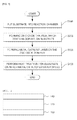
- FIG. 1 is a flowchart illustrating a method of manufacturing a p-type zinc oxide semiconductor thin film according to a preferred embodiment of the present invention.
- FIG. 2 is a cross-sectional view of a p-type zinc oxide semiconductor according to a preferred embodiment of the present invention.
- a substrate 100 is put into a reaction chamber (S100).
- a silicon substrate, a sapphire substrate, a zinc oxide substrate, a flexible polymer substrate, a glass substrate, or a glass substrate on which a transparent conductive oxide is evaporated may be used as the substrate 100.
- a zinc oxide thin film 120 containing a group I or V element is formed (S200).
- a group I element, a group V element, or the oxide of a group V element is used as a dopant in order to form the zinc oxide thin film 120.
- the zinc oxide thin film 120 may be formed by an RF or DC magnetron sputtering method or a pulse laser evaporation method while a solid zinc oxide containing 0.001 to 40% by weight of a phosphorus oxide (P 2 O 5 ) is used as a target.
- P 2 O 5 phosphorus oxide
- a thin film is formed using a source in a plasma state, it is possible to improve the reactivity between a group V element or the oxide of a group V element and a zinc oxide. Therefore, it is possible to increase the amount of the group V element or the oxide thereof that is implanted into the formed zinc oxide thin film 120. As a result, it is possible to improve the doping effect.
- a metal catalyst layer 140 is formed on the zinc oxide thin film 120 containing the dopant (S300).
- the metal catalyst layer 140 is made of at least one selected from Ni, Au, Pt, Pb, Mg, Cu, Zn, Ag, Sc, Co, Rh, Li, Be, Ca, Ru, Ti, Ta, Na, and La, or an alloy thereof. Further, the metal catalyst layer 140 may have a multilayered structure.
- the thickness of the metal catalyst layer 140 be in the range of 0.1 to 1000 nm.
- the metal catalyst layer 140 be formed by an electron beam evaporator (e-beam evaporator), a thermal evaporator, a sputtering evaporator, or a pulse laser evaporator.
- e-beam evaporator electron beam evaporator
- thermal evaporator thermal evaporator
- sputtering evaporator a pulse laser evaporator
- a heat treatment is performed on the substrate 100 where the metal catalyst layer 140 is formed, so that hydrogen atoms are removed from the zinc oxide thin film 120 and the dopant is activated (S400).
- the heat treatment performed on the substrate 100 may be performed in-situ in the chamber for forming the zinc oxide thin film 120, or may be performed in a separate chamber.
- the group I or V element contained in the zinc oxide thin film 120 is activated due to the heat treatment, and serves as a p-type dopant.
- the metal catalyst layer 140 formed on the zinc oxide thin film 120 makes a dopant-H and an O-H complex body, which are formed due to hydrogen that may be adulterated during the growth of the thin film, be effectively dissociated. Accordingly, the group I or V element is easily activated. It is preferable that the heat treatment be performed in a chamber having gas atmosphere including at least one of nitrogen, oxygen, air, and inert gas.
- the temperature in the chamber is maintained at 50 to 1500°C for 1 second to 30 minutes so that the heat treatment is performed on the substrate 100 where the zinc oxide thin film 120 and the metal catalyst layer 140 are sequentially formed.
- FIG. 3 is a graph showing that hydrogen concentration of a zinc oxide thin film is changed in accordance with heat treatment temperature when a metal catalyst layer is used.
- a zinc oxide thin film which is doped with phosphorus or a phosphorus oxide, is formed on a sapphire substrate at a thin film growth temperature of 500°C by the RF magnetron sputtering method by using a zinc oxide compound target containing 0.01% by weight of a phosphorus oxide (P 2 O 5 ).
- the substrate where the zinc oxide thin film is formed is put into the reaction chamber, and a Ni catalyst metal layer having a thickness of 10 nm is formed on the zinc oxide thin film by an electron beam evaporator.
- the pressure in the chamber is maintained at a vacuum pressure of 7 ⁇ 10 -7 Torr in order to activate the p-type zinc oxide thin film that is formed by the above-mentioned method, and the hydrogen concentration of the zinc oxide thin film was measured while the temperature is changed from a normal temperature to 800°C.
- a zinc oxide thin film which is doped with phosphorus or a phosphorus oxide, is formed under the same conditions as described above. Then, a semiconductor thin film without a Ni catalyst metal layer is formed, and a heat treatment is performed at the same vacuum pressure and temperature. After that, the hydrogen concentration of the zinc oxide thin film was measured.
- the hydrogen concentration of the zinc oxide thin film is significantly decreased at a temperature of 300 to 400°C if a Ni metal catalyst layer is formed. Accordingly, it can be seen that the hydrogen concentration of the zinc oxide thin film is rapidly decreased if the metal catalyst layer is formed and the heat treatment is performed.
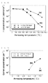
- FIG. 4 is a graph showing how many carriers exist in the zinc oxide thin film when a heat treatment is performed while temperature is changed.
- a zinc oxide thin film doped with phosphorus or a phosphorus oxide is formed, and a heat treatment is then performed at a temperature of a normal temperature to 500°C. It can be seen that hydrogen is not sufficiently diffused to the outside at a temperature lower than 300°C regardless of the formation of the metal catalyst layer, so that the concentration of holes serving as carriers is very low. This is guessed due to a fact that few holes are generated by hydrogen existing in the zinc oxide thin film and a Hall effect for evaluating an electrical characteristic does not sufficiently occur. Accordingly, the doped zinc oxide thin film has a characteristic similar to that of an insulator in a heat treatment performed at a temperature lower than 300°C.
- the zinc oxide thin film doped with phosphorus or a phosphorus oxide is formed and a heat treatment is then performed without forming a metal catalyst layer, it can be seen that the zinc oxide thin film has characteristics substantially similar to those of an insulator at a temperature of 500°C or less regardless of heat treatment temperature.
- the zinc oxide thin film when the zinc oxide thin film doped with phosphorus or a phosphorus oxide is formed and a metal catalyst layer made of Ni is then formed, the zinc oxide thin film has a hole concentration of 2.57 ⁇ 10 14 /cm 3 at a heat treatment temperature of 300°C, that is, an electrical characteristic of a p-type semiconductor. Further, it can be seen that the zinc oxide thin film has a hole concentration of 7.61 ⁇ 10 15 /cm 3 at a heat treatment temperature of 500°C, that is, an electrical characteristic of a highly-concentrated p-type semiconductor.
- the hole concentration is 3.8 ⁇ 10 14 /cm 3 . Comparing the two data, it can be seen that the zinc oxide thin film has a characteristic of a highly-concentrated p-type semiconductor due to the formed metal catalyst layer.
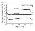
- FIG. 5 is a graph showing the hydrogen concentration in accordance with the depth of the zinc oxide thin film according to the embodiment of the present invention.
- the hydrogen concentration in the zinc oxide thin film is significantly changed depending on whether the metal catalyst layer is formed or not.
- a sample (as grown) where a heat treatment is not performed on a zinc oxide thin film doped with phosphorus or a phosphorus oxide has a hydrogen concentration of about 2 ⁇ 10 20 /cm 3 o
- the hydrogen concentration is about 6 ⁇ 10 19 /cm 3 . Accordingly, it can be seen that the hydrogen concentration of the zinc oxide thin film is decreased to some extent due to a heat treatment.
- a metal catalyst layer is formed on a zinc oxide thin film doped with phosphorus or a phosphorus oxide and a heat treatment is performed at 800°C for 2 minutes, it can be seen that the hydrogen concentration of the thin film is significantly decreased throughout the thin film. That is, it can be seen that the concentration of the zinc oxide thin film is relatively constant regardless of depth and is about 1.5 ⁇ 10 17 /cm 3 .
- the zinc oxide thin film is changed into a zinc oxide thin film, which has an electrical characteristic of a p-type semiconductor, by activating a dopant. Accordingly, the zinc oxide thin film has higher carrier concentration by forming a metal catalyst layer, and is formed as a p-type zinc oxide semiconductor.
- a zinc oxide thin film which has an electrical characteristic of an n-type semiconductor or an electrical characteristic of an insulator, is easily changed into a zinc oxide thin film, which has an electrical characteristic of an p-type semiconductor, by a metal catalyst layer and a heat treatment. Therefore, it is possible to generate and provide holes that are essential for a photoelectric device and an electronic device, so that it is possible to develop a photoelectric device and an electronic device, such as a light emitting diode, a laser diode, and a p-type transparent thin film transistor.
Landscapes
- Physical Vapour Deposition (AREA)
- Thin Film Transistor (AREA)
- Liquid Deposition Of Substances Of Which Semiconductor Devices Are Composed (AREA)
- Photovoltaic Devices (AREA)
Applications Claiming Priority (1)
| Application Number | Priority Date | Filing Date | Title |
|---|---|---|---|
| KR2007063270 | 2007-06-23 |
Publications (2)
| Publication Number | Publication Date |
|---|---|
| EP2009683A2 true EP2009683A2 (de) | 2008-12-31 |
| EP2009683A3 EP2009683A3 (de) | 2011-05-04 |
Family
ID=40076741
Family Applications (1)
| Application Number | Title | Priority Date | Filing Date |
|---|---|---|---|
| EP08104509A Withdrawn EP2009683A3 (de) | 2007-06-23 | 2008-06-23 | Zinkoxidhalbleiter und Verfahren zu seiner Herstellung |
Country Status (1)
| Country | Link |
|---|---|
| EP (1) | EP2009683A3 (de) |
Cited By (3)
| Publication number | Priority date | Publication date | Assignee | Title |
|---|---|---|---|---|
| JP2011124561A (ja) * | 2009-11-13 | 2011-06-23 | Semiconductor Energy Lab Co Ltd | 半導体装置及びその作製方法 |
| JP2017028077A (ja) * | 2015-07-22 | 2017-02-02 | スタンレー電気株式会社 | ZnO系半導体構造の製造方法 |
| JP2018026569A (ja) * | 2009-09-04 | 2018-02-15 | 株式会社半導体エネルギー研究所 | 表示装置の作製方法 |
Citations (4)
| Publication number | Priority date | Publication date | Assignee | Title |
|---|---|---|---|---|
| JP2000244014A (ja) | 1999-02-19 | 2000-09-08 | Murata Mfg Co Ltd | 半導体発光素子、およびその製造方法 |
| JP2002016088A (ja) | 2000-04-19 | 2002-01-18 | Murata Mfg Co Ltd | p型半導体膜の製造方法およびそれを用いた発光素子 |
| KR20020077557A (ko) | 2001-04-02 | 2002-10-12 | 광주과학기술원 | 아연산화물 반도체 제조 방법 |
| WO2007024041A1 (en) | 2005-08-23 | 2007-03-01 | Korea Institute Of Science And Technology | Method of fabricating a p-i-n light emitting diode using cu-doped p-type zno |
Family Cites Families (1)
| Publication number | Priority date | Publication date | Assignee | Title |
|---|---|---|---|---|
| DE60334998D1 (de) * | 2002-08-28 | 2010-12-30 | Moxtronics Inc | Hybridstrahl-beschichtungssystem und verfahren zur herstellung von zno-schichten |
-
2008
- 2008-06-23 EP EP08104509A patent/EP2009683A3/de not_active Withdrawn
Patent Citations (4)
| Publication number | Priority date | Publication date | Assignee | Title |
|---|---|---|---|---|
| JP2000244014A (ja) | 1999-02-19 | 2000-09-08 | Murata Mfg Co Ltd | 半導体発光素子、およびその製造方法 |
| JP2002016088A (ja) | 2000-04-19 | 2002-01-18 | Murata Mfg Co Ltd | p型半導体膜の製造方法およびそれを用いた発光素子 |
| KR20020077557A (ko) | 2001-04-02 | 2002-10-12 | 광주과학기술원 | 아연산화물 반도체 제조 방법 |
| WO2007024041A1 (en) | 2005-08-23 | 2007-03-01 | Korea Institute Of Science And Technology | Method of fabricating a p-i-n light emitting diode using cu-doped p-type zno |
Non-Patent Citations (4)
| Title |
|---|
| C. G. VAN DE WALLE ET AL., NATURE, vol. 423, 2003, pages 626 |
| D. C. LOOK, APPL. PHYS. LETT., vol. 81, 2002, pages 1830 |
| K. K. KIM ET AL., APPL. PHYS. LETT., vol. 83, 2003, pages 63 |
| T. AOKI ET AL., APPL. PHYS. LETT., vol. 76, 2000, pages 3257 |
Cited By (3)
| Publication number | Priority date | Publication date | Assignee | Title |
|---|---|---|---|---|
| JP2018026569A (ja) * | 2009-09-04 | 2018-02-15 | 株式会社半導体エネルギー研究所 | 表示装置の作製方法 |
| JP2011124561A (ja) * | 2009-11-13 | 2011-06-23 | Semiconductor Energy Lab Co Ltd | 半導体装置及びその作製方法 |
| JP2017028077A (ja) * | 2015-07-22 | 2017-02-02 | スタンレー電気株式会社 | ZnO系半導体構造の製造方法 |
Also Published As
| Publication number | Publication date |
|---|---|
| EP2009683A3 (de) | 2011-05-04 |
Similar Documents
| Publication | Publication Date | Title |
|---|---|---|
| US7842539B2 (en) | Zinc oxide semiconductor and method of manufacturing the same | |
| US6852623B2 (en) | Method for manufacturing zinc oxide semiconductors | |
| CN101573804B (zh) | 氮化镓系化合物半导体发光元件及其制造方法 | |
| CN101174667A (zh) | 衬底上的氧化物膜 | |
| JP2001035805A (ja) | Iii族ナイトライド化合物半導体薄膜およびその形成方法、並びに半導体素子およびその製造方法 | |
| KR100432856B1 (ko) | 화합물 반도체 장치의 제조방법 및 화합물 반도체 장치의 제조장치 | |
| US8154018B2 (en) | Semiconductor device, its manufacture method and template substrate | |
| KR102418187B1 (ko) | 금속 칼코겐 화합물 박막의 제조 방법 | |
| JP3945782B2 (ja) | 半導体発光素子及びその製造方法 | |
| EP2009683A2 (de) | Zinkoxidhalbleiter und Verfahren zu seiner Herstellung | |
| KR101458629B1 (ko) | ZnO계 화합물 반도체 층의 제조방법 | |
| KR100947748B1 (ko) | P형의 전기적 특성을 갖는 아연산화물 반도체 제조방법 | |
| CN101235537B (zh) | 制备ZnMgO合金薄膜的方法 | |
| KR20050081207A (ko) | 터널 정션 배리어층을 사용한 단결정 질화물계 반도체 성장및 이를 이용한 고품위 질화물계 발광소자 제작 | |
| CN102498585A (zh) | 半导体发光器件 | |
| US8294146B2 (en) | ZnO-containing semiconductor layer and device using the same | |
| JP2007129271A (ja) | 半導体発光素子及びその製造方法 | |
| TWI315106B (en) | Gallium nitride-based compound semiconductor light-emitting device | |
| KR100293467B1 (ko) | 청색발광소자및그제조방법 | |
| EP2615651A1 (de) | Verfahren zur herstellung eines gruppe-iii-nitrid-halbleiter-lichtemissionselements und gruppe iii-nitrid halbleiter-lichtemissionselement | |
| WO2007015613A1 (en) | Nitride light emitting device of using substrate decomposition prevention layer and manufacturing method of the same | |
| KR102394975B1 (ko) | 반도체 소자의 제조 방법 및 이에 의해 제조된 반도체 소자 | |
| JP2007251027A (ja) | ZnO系化合物半導体、それを用いた発光素子及びそれらの製造方法 | |
| KR20050081208A (ko) | 기판 분해 방지막을 사용한 단결정 질화물계 반도체 성장및 이를 이용한 고품위 질화물계 발광소자 제작 | |
| WO2006085670A1 (ja) | 電極及び化合物半導体素子 |
Legal Events
| Date | Code | Title | Description |
|---|---|---|---|
| PUAI | Public reference made under article 153(3) epc to a published international application that has entered the european phase |
Free format text: ORIGINAL CODE: 0009012 |
|
| 17P | Request for examination filed |
Effective date: 20080623 |
|
| AK | Designated contracting states |
Kind code of ref document: A2 Designated state(s): AT BE BG CH CY CZ DE DK EE ES FI FR GB GR HR HU IE IS IT LI LT LU LV MC MT NL NO PL PT RO SE SI SK TR |
|
| AX | Request for extension of the european patent |
Extension state: AL BA MK RS |
|
| RIN1 | Information on inventor provided before grant (corrected) |
Inventor name: HWANG, DAE KYU Inventor name: KWON, MIN KI Inventor name: OH, MIN SUK Inventor name: PARK, SUNG JOO |
|
| PUAL | Search report despatched |
Free format text: ORIGINAL CODE: 0009013 |
|
| AK | Designated contracting states |
Kind code of ref document: A3 Designated state(s): AT BE BG CH CY CZ DE DK EE ES FI FR GB GR HR HU IE IS IT LI LT LU LV MC MT NL NO PL PT RO SE SI SK TR |
|
| AX | Request for extension of the european patent |
Extension state: AL BA MK RS |
|
| RIC1 | Information provided on ipc code assigned before grant |
Ipc: H01L 21/02 20060101ALI20110328BHEP Ipc: H01L 21/36 20060101AFI20081010BHEP |
|
| AKX | Designation fees paid |
Designated state(s): DE FR GB |
|
| 17Q | First examination report despatched |
Effective date: 20120620 |
|
| STAA | Information on the status of an ep patent application or granted ep patent |
Free format text: STATUS: THE APPLICATION IS DEEMED TO BE WITHDRAWN |
|
| 18D | Application deemed to be withdrawn |
Effective date: 20140102 |