EP2000938A2 - Dispositif de traitement d'informations et procédé d'activation de commande - Google Patents
Dispositif de traitement d'informations et procédé d'activation de commande Download PDFInfo
- Publication number
- EP2000938A2 EP2000938A2 EP08156613A EP08156613A EP2000938A2 EP 2000938 A2 EP2000938 A2 EP 2000938A2 EP 08156613 A EP08156613 A EP 08156613A EP 08156613 A EP08156613 A EP 08156613A EP 2000938 A2 EP2000938 A2 EP 2000938A2
- Authority
- EP
- European Patent Office
- Prior art keywords
- trigger signal
- verification
- information processing
- processing device
- verifying
- Prior art date
- Legal status (The legal status is an assumption and is not a legal conclusion. Google has not performed a legal analysis and makes no representation as to the accuracy of the status listed.)
- Withdrawn
Links
Images

Classifications
-
- G—PHYSICS
- G06—COMPUTING OR CALCULATING; COUNTING
- G06F—ELECTRIC DIGITAL DATA PROCESSING
- G06F21/00—Security arrangements for protecting computers, components thereof, programs or data against unauthorised activity
- G06F21/30—Authentication, i.e. establishing the identity or authorisation of security principals
- G06F21/31—User authentication
- G06F21/34—User authentication involving the use of external additional devices, e.g. dongles or smart cards
-
- G—PHYSICS
- G06—COMPUTING OR CALCULATING; COUNTING
- G06F—ELECTRIC DIGITAL DATA PROCESSING
- G06F21/00—Security arrangements for protecting computers, components thereof, programs or data against unauthorised activity
- G06F21/70—Protecting specific internal or peripheral components, in which the protection of a component leads to protection of the entire computer
-
- G—PHYSICS
- G06—COMPUTING OR CALCULATING; COUNTING
- G06F—ELECTRIC DIGITAL DATA PROCESSING
- G06F21/00—Security arrangements for protecting computers, components thereof, programs or data against unauthorised activity
- G06F21/70—Protecting specific internal or peripheral components, in which the protection of a component leads to protection of the entire computer
- G06F21/81—Protecting specific internal or peripheral components, in which the protection of a component leads to protection of the entire computer by operating on the power supply, e.g. enabling or disabling power-on, sleep or resume operations
-
- G—PHYSICS
- G06—COMPUTING OR CALCULATING; COUNTING
- G06F—ELECTRIC DIGITAL DATA PROCESSING
- G06F2221/00—Indexing scheme relating to security arrangements for protecting computers, components thereof, programs or data against unauthorised activity
- G06F2221/21—Indexing scheme relating to G06F21/00 and subgroups addressing additional information or applications relating to security arrangements for protecting computers, components thereof, programs or data against unauthorised activity
- G06F2221/2153—Using hardware token as a secondary aspect
Definitions
- the present invention relates to an information processing device such as a personal computer, and particularly to an information processing device the system of which can be safely activated by an external device, and also to an activation control method adopted in such a device.
- Jpn. Pat. Appln. KOKAI Publication No. 8-63252 discloses a technology of delivering a wakeup event from the device to a power management module (hereinafter, referred to as "PMM") by bypassing the chipset, with a sideband signal line through which only a pull-up signal can be sent between the device and the PMM.
- PMM power management module
- the system may be started up even when the chipset is not activated.
- the system may be illegally started with a faked signal, creating a security problem.
- the present invention has been conceived in light of the above problem.
- the purpose of the invention is to offer an information processing device and an activation controlling method that both can verify a wakeup signal before activating the system.
- an information processing device which activates the system with a trigger signal sent from a device connected thereto, comprises a receiving section configured to receive the trigger signal from the connected device, and a verifying section configured to verify the trigger signal when the receiving section receives the trigger signal.
- a verifying section configured to verify the trigger signal when the receiving section receives the trigger signal.
- the present invention also offers an activation control method for activating a system with a trigger signal issued by a device connected thereto.
- the method comprises a receiving step in which the trigger signal is received from the connected device, and a verifying step in which the trigger signal is verified when the trigger signal is received in the receiving step.
- verifying step When verification of the trigger signal is successfully made in the verifying step, the system is activated.
- security of the system can be improved by verifying a wakeup event before the activation of the system.
- the structure of an information processing device according to an embodiment of the present invention will be first discussed with reference to FIGS. 1 and 2 .
- the information processing device is realized here in the form of a notebook personal computer 10.
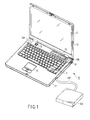
- FIG. 1 shows a perspective view of the notebook personal computer 10 with its display unit open.
- the computer 10 comprises a computer main unit 11 and a display unit 12.
- a display device formed of a thin film transistor liquid crystal display (TFT-LCD) 17 is incorporated in the display unit 12, and the display screen of the LCD 17 is positioned substantially in the center of the display unit 12.
- TFT-LCD thin film transistor liquid crystal display
- the display unit 12 is arranged on the computer main unit 11 rotatably between an open position and a close position.
- the computer main body 11 is a thin box housing, on top of which a keyboard 13, a power switch 14 for turning on/off the computer 10, an input operation panel 15, a touch pad 16, and a pair of speakers 18A and 18B.
- the input operation panel 15 is an input device for inputting an event in correspondence with a pressed button, and has different buttons to activate different functions.
- a device 400 is connected to the computer 10 by way of a USB cable 402, which is connected to a later-described USB host controller 403.
- This device 400 conforms to the USB standards.
- the computer 10 comprises a CPU 111, a north bridge 112, a main memory 113, a south bridge 115, a graphics controller 114, BIOS-ROM 118, a network controller 117, a hard disk drive (HDD) 116, an embedded controller/keyboard controller (EC/KBC) 119, a power supply circuit 120, and the like.
- the CPU 111 is a processor that controls the operation of the computer 10 and executes the operating system and various applications loaded from the HDD 116 into the main memory 113.
- the CPU 111 also executes the Basic Input/Output System (BIOS) stored in the BIOS-ROM 118.
- BIOS is a hardware controlling program.
- the north bridge 112 is a bridge device bridging the local bus of the CPU 111 and the south bridge 115.
- the north bridge 112 includes a memory controller that controls the access to the main memory 113.
- the north bridge 112 also conducts communications with the graphics controller 114 by way of a PCI Express serial bus or the like.
- the graphics controller 114 is a display controller that controls the LCD 17 employed as a display monitor of the computer 10. A display signal generated by the graphics controller 114 is sent to the LCD 17.
- the south bridge 115 controls devices on the low pin count (LPC) bus and on the peripheral component interconnect (PCI) bus.
- the south bridge 115 includes an integrated drive electronics (IDE) controller to control the HDD 116.
- IDE integrated drive electronics
- the embedded controller/keyboard controller (EC/KBC) 119 is a one-chip microcomputer in which an embedded controller for managing power supply and a keyboard controller for controlling the keyboard (KB) 13 and the touch pad 16 are integrated.
- the EC/KBC 119 turns the computer 10 on/off in accordance with the user's operation of the power switch 14.
- the device 400 is connected to the computer 10 by way of the USB cable 402 via the USB host controller 403 that is connected on the PCI bus.
- the device 400 is also connected to a sideband 401, which is a line specially designed to transmit a pull-up signal (trigger signal) to the EC/KBC 119.
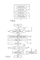
- FIG. 3 is a block diagram of the functional structure of the information processing device according to the embodiment of the present invention.
- a controlling section 20, a memory section 21, a verifying section 22, and a receiving section 23 are included as functional sections in the embodiment of the information processing device according to the present invention.
- the controlling section 20 is the CPU 111, which controls the entire system.
- the memory section 21 is a flash memory that stores verification information and encryption information (such as encryption keys). The information may be stored in the BIOS-ROM 118.
- the verifying section 22 is the BIOS-ROM 118, which verifies the trigger signals and devices.
- the receiving section 23 is the EC/KBC 119 and the USB host controller 403 that exchange signals with the device 400.
- the EC/KBC 119 monitors reception of a pull-up signal, which is a trigger signal from the device 400 (step S101).
- a pull-up signal that is a trigger signal is received from the device 400 (Yes in step S101)
- the EC/KBC 119 starts preparing the activation of the system (personal computer 10) (step S102).
- the chipset is activated (step S103).
- the BIOS is activated (step S104).
- the BIOS (verifying section) checks with the device 400 by way of the chipset to determine whether the pull-up signal that is a trigger signal has been transmitted (signal verification) (step S105).
- the BIOS confirms with the device 400 in step S105 that the pull-up signal that is a trigger signal has been transmitted (signal verification successfully made, Yes in step S105)
- the system is activated (step S106).
- the BIOS cannot confirm with the device 400 that the pull-up signal that is a trigger signal has been transmitted (failure of signal verification, No in step S105)
- the signal is considered as being illegally fabricated.
- the system is shut down (step S107). Instead of shutting down, the system may be put into a sleep mode, a suspend mode, or a lock mode.
- the signals may be encrypted.
- a pull-up signal received from a USB-connected device is verified as discussed above, and thus the system can be prevented from being activated by an illegal pull-up signal, and security can be improved.
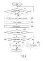
- Steps S201 through S205 in FIG. 5 are the same as steps S101 through S105 in FIG. 4 .
- step S205 device verification is conducted for the device 400.
- the BIOS checks with the device 400 to determine whether the pull-up signal that is a trigger signal has been transmitted (signal verification) (step S206).
- step S206 the system is activated (step S207).
- step S208 the device verification made for the device 400 by the BIOS is not successful in step S205 (No in step S205)
- the device is considered illegal, and the system is shut down (step S208).
- step S208 when the signal verification made by the BIOS is not successful in step S206 (No in step S206), the device is considered illegal, and the system is shut down (step S208). Instead of shutting down, the system may be put into a sleep mode, a suspend mode, or a lock mode. Furthermore, when exchanging signals during the signal verification, the signals may be encrypted. When exchanging signals during the device verification for the device 400, the signals may also be encrypted.
- the present invention is not limited to the above embodiment and modification example, but can be realized, when it is implemented, by modifying the structural components within the scope of the invention.
- various combinations of the structural components disclosed above can provide various inventions. For instance, some of the structural components may be omitted from the embodiment or the modification example, or the structural components in the embodiment and the modification example may be suitably combined.
Landscapes
- Engineering & Computer Science (AREA)
- Theoretical Computer Science (AREA)
- Computer Hardware Design (AREA)
- Computer Security & Cryptography (AREA)
- Software Systems (AREA)
- Physics & Mathematics (AREA)
- General Engineering & Computer Science (AREA)
- General Physics & Mathematics (AREA)
- Storage Device Security (AREA)
- Stored Programmes (AREA)
Applications Claiming Priority (1)
| Application Number | Priority Date | Filing Date | Title |
|---|---|---|---|
| JP2007142202A JP4970144B2 (ja) | 2007-05-29 | 2007-05-29 | 情報処理装置および起動制御方法 |
Publications (1)
| Publication Number | Publication Date |
|---|---|
| EP2000938A2 true EP2000938A2 (fr) | 2008-12-10 |
Family
ID=39707992
Family Applications (1)
| Application Number | Title | Priority Date | Filing Date |
|---|---|---|---|
| EP08156613A Withdrawn EP2000938A2 (fr) | 2007-05-29 | 2008-05-21 | Dispositif de traitement d'informations et procédé d'activation de commande |
Country Status (3)
| Country | Link |
|---|---|
| US (1) | US8645705B2 (fr) |
| EP (1) | EP2000938A2 (fr) |
| JP (1) | JP4970144B2 (fr) |
Families Citing this family (2)
| Publication number | Priority date | Publication date | Assignee | Title |
|---|---|---|---|---|
| US20110102157A1 (en) * | 2009-11-05 | 2011-05-05 | Nokia Corporation | Wake-Up For Wireless Devices Based On Requested Data |
| JP7356483B2 (ja) | 2021-10-18 | 2023-10-04 | 株式会社日立製作所 | 情報処理装置、真正性検証方法、及びプログラム |
Family Cites Families (15)
| Publication number | Priority date | Publication date | Assignee | Title |
|---|---|---|---|---|
| JPH0863252A (ja) | 1994-08-26 | 1996-03-08 | Nec Shizuoka Ltd | 情報処理装置の起動方式 |
| US6105140A (en) * | 1998-02-10 | 2000-08-15 | Compaq Computer Corporation | Secure power supply |
| JPH11345205A (ja) * | 1998-06-03 | 1999-12-14 | Toshiba Corp | コンピュータシステムおよびそのウェイクアップ制御方法 |
| JPH11353266A (ja) | 1998-06-10 | 1999-12-24 | Toshiba Corp | コンピュータシステムおよび同システムの状態制御方法 |
| US6311276B1 (en) * | 1998-08-25 | 2001-10-30 | 3Com Corporation | Secure system for remote management and wake-up commands |
| US6526507B1 (en) * | 1999-02-18 | 2003-02-25 | International Business Machines Corporation | Data processing system and method for waking a client only in response to receipt of an authenticated Wake-on-LAN packet |
| KR100342021B1 (ko) | 1999-03-12 | 2002-06-27 | 윤종용 | 원격 조정되는 컴퓨터 시스템 및 그것의 작동 방법 |
| JP2003084981A (ja) | 2001-09-11 | 2003-03-20 | Seiko Epson Corp | 情報処理装置の起動方法 |
| JP2003150268A (ja) * | 2001-11-14 | 2003-05-23 | Nec Gumma Ltd | コンピュータのセキュリティシステム及び電源制御装置 |
| US20050166213A1 (en) * | 2003-12-31 | 2005-07-28 | International Business Machines Corporation | Remote deployment of executable code in a pre-boot environment |
| US7086583B2 (en) * | 2004-01-20 | 2006-08-08 | Standard Microsystems Corporation | Systems and methods for power reduction in systems having removable media devices |
| JP2006252329A (ja) | 2005-03-11 | 2006-09-21 | Toshiba Corp | 情報処理装置および起動制御方法 |
| US7725194B2 (en) * | 2005-08-30 | 2010-05-25 | Boston Scientific Neuromodulation Corporation | Telemetry-based wake up of an implantable medical device |
| KR100703215B1 (ko) * | 2006-02-20 | 2007-04-09 | 삼성전기주식회사 | 저전력 무선통신기기 및 저전력 무선통신 방법 |
| CN100561926C (zh) * | 2006-09-30 | 2009-11-18 | 联想(北京)有限公司 | 一种基于wan模块的远程唤醒系统及终端 |
-
2007
- 2007-05-29 JP JP2007142202A patent/JP4970144B2/ja active Active
-
2008
- 2008-05-20 US US12/124,075 patent/US8645705B2/en active Active
- 2008-05-21 EP EP08156613A patent/EP2000938A2/fr not_active Withdrawn
Also Published As
| Publication number | Publication date |
|---|---|
| US8645705B2 (en) | 2014-02-04 |
| US20080301423A1 (en) | 2008-12-04 |
| JP4970144B2 (ja) | 2012-07-04 |
| JP2008299417A (ja) | 2008-12-11 |
Similar Documents
| Publication | Publication Date | Title |
|---|---|---|
| US8255725B2 (en) | Information processing apparatus and power-saving control method | |
| CN103207975B (zh) | 保护密码的方法以及计算机 | |
| CN102955921B (zh) | 电子装置与安全开机方法 | |
| US10671731B2 (en) | Method, apparatus, and medium for using a stored pre-boot authentication password to skip a pre-boot authentication step | |
| US20070180255A1 (en) | Information processing apparatus and authentication control method | |
| CN100485705C (zh) | 信息处理设备和验证控制方法 | |
| JP4185104B2 (ja) | 情報機器及びその動作制御方法 | |
| WO2016209353A1 (fr) | Authentification d'une connexion à protocoles multiples | |
| CN101751534A (zh) | 具备生物认证装置的计算机 | |
| JP2004234331A (ja) | 情報処理装置および同装置で使用されるユーザ操作制限方法 | |
| JP2014010492A (ja) | 情報処理装置および起動制御方法 | |
| JP2015001800A (ja) | スリープ状態からレジュームする方法、携帯式電子機器およびコンピュータ・プログラム | |
| JP4846862B2 (ja) | 情報処理装置および省電力制御方法 | |
| US8645705B2 (en) | Information processing device and activation control method | |
| EP2073492B1 (fr) | Gestion du verrouillage de carte SIM par un opérateur de réseau | |
| JP2009015377A (ja) | 情報処理装置 | |
| JP5006089B2 (ja) | 情報処理装置 | |
| JP4247216B2 (ja) | 情報処理装置および認証制御方法 | |
| JP5367684B2 (ja) | セキュリティを強化したコンピュータおよび電源の制御方法 | |
| CN101382974A (zh) | 电脑系统与其安全开机方法 | |
| JP2008299418A (ja) | 情報処理装置および起動制御方法 | |
| JPH11345205A (ja) | コンピュータシステムおよびそのウェイクアップ制御方法 | |
| JP4709778B2 (ja) | 情報処理装置および録画制御方法 | |
| JP2008158763A (ja) | 情報処理装置およびセキュリティ方法 | |
| JP2009075878A (ja) | 情報処理装置、およびオペレーティングシステムのブート方法 |
Legal Events
| Date | Code | Title | Description |
|---|---|---|---|
| PUAI | Public reference made under article 153(3) epc to a published international application that has entered the european phase |
Free format text: ORIGINAL CODE: 0009012 |
|
| 17P | Request for examination filed |
Effective date: 20080521 |
|
| AK | Designated contracting states |
Kind code of ref document: A2 Designated state(s): AT BE BG CH CY CZ DE DK EE ES FI FR GB GR HR HU IE IS IT LI LT LU LV MC MT NL NO PL PT RO SE SI SK TR |
|
| AX | Request for extension of the european patent |
Extension state: AL BA MK RS |
|
| STAA | Information on the status of an ep patent application or granted ep patent |
Free format text: STATUS: THE APPLICATION HAS BEEN WITHDRAWN |
|
| 18W | Application withdrawn |
Effective date: 20090605 |