EP1997134B1 - Vorrichtung und verfahren zum detektieren von defekten in einem wafer unter verwendung einer zeilensensorkamera - Google Patents
Vorrichtung und verfahren zum detektieren von defekten in einem wafer unter verwendung einer zeilensensorkamera Download PDFInfo
- Publication number
- EP1997134B1 EP1997134B1 EP07708823.5A EP07708823A EP1997134B1 EP 1997134 B1 EP1997134 B1 EP 1997134B1 EP 07708823 A EP07708823 A EP 07708823A EP 1997134 B1 EP1997134 B1 EP 1997134B1
- Authority
- EP
- European Patent Office
- Prior art keywords
- wafer
- defect
- inspection
- image
- region
- Prior art date
- Legal status (The legal status is an assumption and is not a legal conclusion. Google has not performed a legal analysis and makes no representation as to the accuracy of the status listed.)
- Not-in-force
Links
Images




Classifications
-
- G—PHYSICS
- G01—MEASURING; TESTING
- G01R—MEASURING ELECTRIC VARIABLES; MEASURING MAGNETIC VARIABLES
- G01R31/00—Arrangements for testing electric properties; Arrangements for locating electric faults; Arrangements for electrical testing characterised by what is being tested not provided for elsewhere
- G01R31/28—Testing of electronic circuits, e.g. by signal tracer
- G01R31/302—Contactless testing
- G01R31/308—Contactless testing using non-ionising electromagnetic radiation, e.g. optical radiation
- G01R31/311—Contactless testing using non-ionising electromagnetic radiation, e.g. optical radiation of integrated circuits
-
- H—ELECTRICITY
- H10—SEMICONDUCTOR DEVICES; ELECTRIC SOLID-STATE DEVICES NOT OTHERWISE PROVIDED FOR
- H10P—GENERIC PROCESSES OR APPARATUS FOR THE MANUFACTURE OR TREATMENT OF DEVICES COVERED BY CLASS H10
- H10P74/00—Testing or measuring during manufacture or treatment of wafers, substrates or devices
-
- G—PHYSICS
- G01—MEASURING; TESTING
- G01N—INVESTIGATING OR ANALYSING MATERIALS BY DETERMINING THEIR CHEMICAL OR PHYSICAL PROPERTIES
- G01N21/00—Investigating or analysing materials by the use of optical means, i.e. using sub-millimetre waves, infrared, visible or ultraviolet light
- G01N21/84—Systems specially adapted for particular applications
- G01N21/88—Investigating the presence of flaws or contamination
- G01N21/95—Investigating the presence of flaws or contamination characterised by the material or shape of the object to be examined
- G01N21/9501—Semiconductor wafers
- G01N21/9505—Wafer internal defects, e.g. microcracks
-
- G—PHYSICS
- G06—COMPUTING OR CALCULATING; COUNTING
- G06V—IMAGE OR VIDEO RECOGNITION OR UNDERSTANDING
- G06V10/00—Arrangements for image or video recognition or understanding
- G06V10/10—Image acquisition
Definitions
- the present invention relates to an apparatus and method for detecting defects in a wafer, and more particularly, to an apparatus and method for detecting positions and sizes of defects existing in a wafer or on its surface.
- a wafer is manufactured through a plurality of subdivided processes, and defects may be generated inside the wafer or on its surface during each process. Such defects may be classified into inherent defects such as cracks in a material itself, and external defects such as foreign substances attached to the wafer surface or contained therein. Defects generated during a process of manufacturing the wafer, depending on their positions and sizes, may result in the wafer having to be discarded. In particular, an air-pocket, a type of molding defect existing in an ingot, may be transferred to a bare wafer manufactured by slicing the ingot. In most cases, a wafer manufactured using a bare wafer having an air-pocket has to be discarded. Therefore, defects should be effectively detected at an appropriate time during the wafer manufacturing process.
- One method of inspecting a wafer for defects is a reflective illumination method whereby light is radiated onto a wafer, reflected by the wafer, and detected using a line scan camera or an area camera.
- this inspection method uses reflected light, a light source that emits with high linearity and intensity should be employed, and the illumination of a work space where the inspection apparatus is installed may have an effect on defect detection results.
- the inspection apparatus since the light source and the camera are disposed on the same space, the inspection apparatus may be quite large.
- Another method of inspecting a wafer for defects is a transmissive illumination method whereby infrared radiation is modified according to characteristics of a wafer through which it is transmitted and detected using an infrared camera.
- An inspection apparatus using a transmissive illumination method is disclosed in U.S. Patent No. 5,981,949 .
- US patent application publication No. US 2003/0210391 describes a pattern defect inspection apparatus capable of detecting defects without being affected by a non-uniform thickness of a thin film formed on a sample.
- the apparatus comprises a laser to illuminate a sample, coherence suppression optics to reduce laser beam coherence, a condenser means to condense the laser beam onto a pupil plane of an objective lens, and a detector means to detect the light reflected from a circuit pattern formed on a sample.
- the condenser means is designed so that light intensity illuminating the sample under test can be partially adjusted according to the type of laser beam illumination condensed on the pupil of the objective lens.; Variations in reflected light intensity caused by non-uniform film thickness on the surface of the sample are therefore reduced and shading minimized in the detected image to allow detecting fine defects.
- US patent application publication No. US 2005/0219521 describes examination devices and methods for examination of wafers.
- the substrate holder is configured so that an illumination device is integrated into the substrate holder in such a way that transmitted light illumination of the wafer is possible.
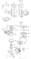
- FIG. 1 is a view of a conventional wafer defect inspection apparatus using a transmissive illumination method.
- the conventional wafer inspection apparatus includes a light source 10, a diffusion plate 14, an optical filter 13, a wafer fixing part 20, an infrared camera 22, a controller 28, a frame grabber 30, a computer 32, and a monitor 26.
- the light source 10 is disposed opposite to one surface of the wafer 18 mounted on the wafer fixing part 20 to radiate light onto the wafer 18.
- the diffusion plate 14 is d isposed between the light source 10 and the wafer 18 to uniformly distribute infrared light radiated from the light source 10.
- the optical filter 13 outputs only infrared wavelengths of the light output from the diffusion plate 14 to the wafer 18, or outputs only infrared wavelengths of the light output from the wafer 18 to the infrared camera 22.
- the infrared camera 22 is disposed opposite to the other side of the wafer 18 to detect the infrared light transmitted through the wafer 18 and output an image thereof.
- the controller 28 controls operation of the infrared camera 22, and selectively outputs an image input from the infrared camera 22 to the monitor 26 or the frame grabber 30.
- the frame grabber 30 digitizes the image input from the controller 28 and outputs the digitized image.
- the computer 32 analyzes the digitized image input from the frame grabber 30 to determine optical characteristics, defect density, and uniformity of the wafer.
- the conventional wafer inspection apparatus having the above constitution can be manufactured to have a simple structure and a compact size, and a single wafer can be inspected within two minutes.
- the time consumed in inspecting a single wafer is much longer than when using an indirect illumination method, thus making it difficult to apply in an actual manufacturing process.
- a plane array infrared camera capable of obtaining an image through a single photographing process and a diffusion plate having an optical transmissivity of 20% - 60% are used, in order to obtain an image sufficient to detect defects in a wafer, a high-energy infrared light source should be used.
- the present invention provides a wafer defect detection apparatus and method capable of rapidly detecting defects in a wafer using a relatively small amount of infrared light.
- the present invention also provides a wafer defect detection apparatus and method capable of rapidly detecting defects in a wafer using a relatively small amount of infrared light by minimizing attenuation of input infrared light and uniformly distributing the infrared light.
- the present invention also provides a wafer defect detection apparatus and method capable of rapidly detecting defects in a wafer using a relatively small amount of infrared light by readily adjusting uniformity of illumination when luminous intensity output from a light source is reduced as a result of changing the light source or lapse of time.
- an apparatus for detecting defects in a wafer is defined in claim 1.
- An apparatus comprising
- a method of detecting defects in the wafer comprises (a) positioning a wafer to be inspected in an inspection region on an inspection stage, the inspection region being formed of a transmissive material;
- FIG. 2 is an exploded perspective view of an apparatus for detecting defects in a wafer in accordance with an exemplary embodiment of the present invention.
- an apparatus 200 for detecting defects in a wafer in accordance with the present invention includes an inspection stage 210, an optical part 220, an image obtaining part 230, a conveying part 240, a controller 250, a defect detection part 260, and an image output part 270.
- the inspection stage 210 has an inspection region on which a wafer 290 to be inspected is disposed.
- the inspection region has an area corresponding to the size of the wafer 290, and is formed of a transparent material such as glass.
- the inspection stage 210 may have a through-hole having a diameter corresponding to the size of the wafer 290 and acting as the inspection region. At this time, the air in the through-hole acts as a transparent material.
- the optical part 220 is disposed under the inspection stage 210 to radiate infrared light onto the wafer 290 to be inspected.
- the optical part 220 includes an infrared lamp 310, a collecting mirror 320, a positioning stage 330, a reflecting mirror 340, a cold mirror 350, a fly-eye lens 360, a collecting lens 370, and an optical uniformity adjustment part 380.
- the infrared lamp 310 emits infrared light having a wavelength of 750 - 850nm, and more preferably 790nm.
- the infrared lamp 310 may be a halogen lamp.
- the collecting mirror 320 reflects the infrared light emitted from the infrared lamp 310 to converge the infrared light in one direction.
- the infrared lamp 310 and the collecting mirror 320 are fixed to the positioning stage 330, and the positioning stage 330 includes x, y and z stages movable in three axial directions constituting an orthogonal coordinate system. Positions of the infrared lamp 310 and the collecting mirror 320 may be changed by movement of the positioning stage 330.
- the reflecting mirror 340 changes an optical path of the infrared light emitted from the infrared lamp 310 and the infrared light reflected by the collecting mirror 320. By changing the optical path using the reflecting mirror 340, the apparatus can be minimized. When the infrared lamp 310 is installed opposite to the inspection stage 210, the reflecting mirror 340 may be unnecessary.
- the cold mirror 350 reflects visible wavelengths of the infrared light output from the infrared lamp 310 and selectively transmits only infrared wavelengths.
- the fly-eye lens 360 includes a first fly-eye lens comprised of a plurality of fine lens cells having rectangular cross-sections and disposed in a matrix to divide the infrared light emitted from the infrared lamp 310 into fine lens cell units and output the divided light, and a second fly-eye lens comprised of a plurality of fine lens cells having rectangular cross-sections and disposed in a matrix to convert the divided light input from the first fly-eye lens into parallel light and output the parallel light.
- FIG. 3 is a view showing optical distribution of an effective light source formed by the fly-eye lens 360.
- the collecting lens 370 concentrates the infrared light transmitted through the fly-eye lens 360 onto the wafer 290.
- the cold mirror 350 among the above components of the optical part 220 is optional.
- the optical uniformity adjustment part 380 improves uniformity of light radiated onto the wafer 290 by driving the positioning stage 330 to change the position of the infrared lamp 310 when a deviation between grey scale values (brightness of an image ranging from 0 to 255) of a plurality of partial images detected from an inspection image generated from a sample wafer having no defect exceeds a predetermined reference value.
- Each of the partial images is formed of a single pixel or a plurality of pixels.
- an average value or an intermediate value of grey scale values of the pixels constituting the partial image is set as a grey scale value of the partial image.
- the deviation between the grey scale values of the partial images may be taken as the difference between the highest and the lowest of the grey scale values, the largest difference between the average of the grey scale values of the partial images and grey scale values of the respective partial images, or may be calculated by some other method.
- the reference value may be set depending on a method of calculating a deviation between the respective grey scale values of the partial images in different manners.
- the reference value may be set such that the difference is within 5% of the average value.
- the optical uniformity adjustment part 380 drives the positioning stage 330 to change the position of the infrared lamp 310.
- movement of the positioning stage 330 by the optical uniformity adjustment part 380 is determined by coordinates of the partial images. That is, as shown in FIG.
- the optical uniformity adjustment part 380 moves the positioning stage 330 by a distance corresponding to the difference between the highest and the lowest of the grey scale values in a positive y-axis direction (or a positive y-axis direction and a positive z-axis direction).
- x- and y-axes of the positioning stage 330 are set to correspond to x-and y-axes on the coordinate system set to the inspection image of the sample wafer, and a positive z-axis direction is set to correspond to a direction in which the positioning stage 330 moves toward the reflecting mirror 340.
- an operator may manually improve optical uniformity using the positioning stage 330.
- the operator functions as the optical uniformity adjustment part 380.
- the operator changes the position of the positioning stage 330 on the basis of a brightness difference recognized from the inspection image generated from the sample wafer having no defect output through the image output part 280, thereby improving optical uniformity.
- the optical uniformity adjustment part 380 may be employed.
- the optical uniformity adjustment part 380 outputs a deviation between the respective grey scale values of the partial images detected from the inspection image, or movement to each axis of the positioning stage 330 calculated on the basis of the deviation between the grey scale values, to the image output part 280.
- the operator changes the position of the positioning stage 330 on the basis of information output through the image output part 280 to improve optical uniformity.
- the optical part 220 may be implemented using a linear light guide.
- FIGS. 5 and 6 show an example of the optical part 220 employing a linear light guide.
- the optical part 220 includes a light source 510, an optical transmission path 530, and a linear light guide 530.
- the light source 510 includes an infrared lamp 512, a reflecting mirror 514, and a housing 516.
- the infrared lamp 512 emits infrared light having a wavelength of 750 - 850nm, and more preferably 790nm.
- a reflecting mirror 514 is installed at the rear end of the infrared lamp 512 to collect light emitted from the infrared lamp 512 into one side of the housing 516.
- the infrared lamp 512 may be a halogen lamp.
- the housing 516 has a space for accommodating the infrared lamp 512.
- the optical transmission path 520 is fixedly inserted into one side of the housing 516.
- the optical transmission path 520 fixed to the housing 516 is formed of an optical fiber coated with an optical blocking coating material or an optical waveguide.
- the linear light guide 530 converts the infrared light transmitted through the optical transmission path 520 into a line of light and outputs the line of light. By employing the linear light guide 530, there is no need to perform optical alignment when changing the infrared lamp 512. In addition, since light is transmitted through the optical fiber or optical waveguide, there is no need to dispose lenses on an optical path, thereby reducing overall manufacturing cost.
- optical uniformity of the infrared light converted into the line of light through the optical fiber or the optical waveguide of the linear light guide 530 is within the ⁇ 8% minimum uniformity required to inspect the wafer, performance reduction of the optical part is small compared to the optical part shown in FIG. 2 .
- the image obtaining part 230 includes a plurality of line sensors having a striped photographing region, and detects infrared light transmitted through the wafer 290 disposed on the inspection stage 210 to output an obtained image signal.
- the image obtaining part 230 is installed at a position spaced apart from the wafer 290 by a pre-determined distance, and a plurality of line sensors are disposed in parallel with each other.
- Each of the line sensors is formed of 8000 pixels and obtains an image with a resolution of 6 micrometers. Therefore, a photographing region of each line sensor has a long side of 48mm. In order to obtain the entire image of a wafer having a diameter of 200mm, at least five scans are required.
- FIG. 7 is a diagram showing positions of a plurality of line sensors installed in an image obtaining part 230.
- the conveying part 240 conveys the image obtaining part 230 or the inspection stage 210 in a short-side direction of the photographing region of the line sensor, and outputs a pulse signal having a predetermined period corresponding to a relative straight moving distance between the image obtaining part 230 and the inspection stage 210.
- a conveyance speed of the conveying part 240 is varied depending on light intensity. When the intensity of the infrared light radiated onto the wafer 290 is 50mW, the conveyance speed may be set as 40mm/sec.
- the controller 250 counts the pulse signal input from the conveying part 240, and outputs a photographing instruction signal for controlling to photograph the wafer 290 using the image obtaining part 230 whenever the wafer 290 is conveyed in a short-side direction of the photographing region of the line sensor toward the image obtaining part 230 by a distance corresponding to the length of the short side of the photographing region.
- a signal having a certain period such as an encoder pulse may be used as a trigger signal for synchronizing a conveyance time of the wafer 290 or the image obtaining part 230 with an output time of the photographing instruction signal.
- the encoder pulse it is possible to maintain a region of a single line scanned by the line sensor at predetermined intervals.
- the pulse signal input from the conveying part 240 to the controller 250 corresponds to a trigger signal.
- the photographing instruction signal may be generated by a frame grabber.
- the frame grabber counts a trigger signal input from the conveying part 240 and generates a photographing synchronization signal in a pulse form to output the synchronization signal when the number of trigger signals corresponds to the wafer 290 conveyed by a distance corresponding to the length of the short side of the photographing region of the line sensor.
- the photographing synchronization signal generated by the frame grabber is input to the image obtaining part 230 as a photographing instruction signal.
- the frame grabber may be implemented as one component of the controller 250, or disposed between the conveying part 240 and the controller 250 as a separate component from the controller 250.
- FIG. 8 is a diagram showing an image obtaining process of the image obtaining part 230 depending on movement of the wafer 290 to be inspected.
- the image obtaining part 230 is comprised of four line sensors S1 to S4, and photographing regions L1 to L8 corresponding to the line sensors are formed on the wafer 290 to be inspected.
- the first line sensor S1 photographs the first photographing region L1 on the wafer 290.
- the first line sensor S1 transmits charges accumulated therein (i.e., charges accumulated by infrared light detected from the first photographing region L1) to the second line sensor S2 and then photographs the second photographing region L2.
- the second line sensor S2 accumulates the charges accumulated by the infrared light detected from the first photographing region L1 and the charges transmitted from the first line sensor S1.
- Each of the line sensors S 1 to S4 repeatedly performs transmission and accumulation of the charges accumulated according to the photographing instruction signal until photographing of the entire wafer 290 is completed in the manner described above.
- the fourth line sensor S4 outputs the charges accumulated therein as an image signal of the wafer 290 from the time when the photographing instruction signal is input after exceeding the number of line sensors S1 to S4 (i.e., when a fifth photographing instruction signal is input).
- An image signal output from the fourth line sensor S4 i.e., an output signal of the image obtaining part 230
- the image obtaining process described with reference to FIG. 8 is performed by a line sensor camera including a plurality of line sensors employed as the image obtaining part 230, even when a time delay and integration (TDI) line scan camera is employed as the image obtaining part 230, the image may be obtained in the same manner as described above.
- the TDI line scan camera including several tens of line sensors can transmit charges accumulated in each line sensor to adjacent line sensors as the line sensors move relative to an object to obtain a charge accumulation effect corresponding to the number of line sensors, so that the TDI line scan camera can obtain an image of approximately one hundred times higher sensitivity than a general line scan camera under the same conditions.
- the TDI line scan camera is used, even though low-intensity infrared light is radiated, it is possible to rapidly detect the light transmitted through the wafer.
- FIG. 9 is a diagram of signals output from line sensors depending on photographing instruction signals.
- each of the line sensors S1 to S4 detects infrared light input from the corresponding photographing region on the wafer 290 to accumulate charges whenever a synchronization signal (i.e., a photographing instruction signal) is input.
- the fourth line sensors S4 outputs the accumulated charges to the defect detection part 260 when an eighth (a multiple of four) synchronization signal is input.
- An output signal of the line sensor of FIG. 7 is represented as S ij (L k ).
- i ranges from 1 to 1(1 is the number of line sensors)
- k is the number of photographing regions on the wafer
- the defect detection part 260 combines image signals input from the image obtaining part 230 to generate an inspection image corresponding to the wafer 290, and detects positions and sizes of defects (i.e., particles or air-pockets) existing in the wafer 290 from the generated inspection image.
- the defect detection part 260 can detect whether the wafer 290 is good or bad on the basis of the number of defects detected, as well as the positions and sizes of the defects existing in the wafer 290.
- a reference value for determining whether the wafer 290 is good or bad is pre-set.
- FIG. 10 is a block diagram of the defect detection part 260.
- the defect detection part 260 includes an inspection image generating part 262 and a defect determination part 264.
- the inspection image generating part 262 combines image signals input from the image obtaining part 230 to generate an inspection image corresponding to the wafer 290.
- the defect determination part 264 determines the region in which the absolute value of the difference between a grey scale value of pixels constituting an inspection image generated by the inspection image generating part 262 and a pre-set reference grey scale value is larger than a predetermined reference value (for example, ⁇ 30 with reference to a grey scale value of a reference image obtained from a wafer having no defect), as a defect region.
- the grey scale value is in the range of 0 - 255 depending on brightness.
- the positions of the defects are represented as coordinates on a coordinate system set with respect to an inspection image of the sample wafer as shown in FIG. 6 .
- the apparatus may be configured to allow the defect determination part 264 to detect a defect in the wafer 290 only when there is a defect region having a diameter larger than a predetermined diameter (e.g., 30 ⁇ ), among the determined defect regions.
- a predetermined diameter e.g. 30 ⁇
- the image output part 270 outputs an inspection image, position and size information of the defects, and an enlarged image of the defect, which are generated by the defect detection part 260.
- the image output part 270 outputs information on a current state of the wafer defect detection apparatus 200, a user interface screen, and so on. Therefore, an operator can control processes of driving the apparatus and inspecting defects on the basis of information output through the image output part 270.
- FIGS. 11 and 12 are views of an example of a user interface screen of an inspection image output to the image output part 270, and an enlarged image of an air-pocket detected in the wafer, respectively.
- FIG. 13 is a plan view of an apparatus for detecting defects in a wafer in accordance with another exemplary embodiment of the present invention.
- an apparatus 1100 for detecting defects in a wafer in accordance with the present invention includes a wafer conveying part 1110, a first cassette 1120, a second cassette 1130, an alignment part 1140, an optical character reading part 1150, a detection result storage part 1160, and a detection result transmission part 1170, in addition to the components of the wafer defect detection apparatus 200 described with reference to FIG. 2 .
- a wafer defect detection apparatus 200 already described with reference to FIG. 2 will not be repeated and those components will be designated by the same reference numerals as in FIG. 2 .
- the wafer conveying part 1110 extracts a wafer 290 to be inspected from a supply cassette in which wafers are mounted, conveys the wafer 290 onto an inspection region on an inspection stage 210, and removes the wafer 290 from the inspection region after completion of defect inspection of the wafer 290 by a defect detection part 260.
- the first cassette 1120 accommodates wafers 290 determined to have defects and the second cassette 1130 accommodates wafers 290 determined to have no defects.
- Each of the first cassette 1120 and the second cassette 1130 may be comprised of a plurality of cassettes.
- the wafer 290 removed from the inspection region after the inspection is conveyed to and accommodated in the first cassette 1120 or the second cassette 1130 using the wafer conveying part 110.
- the alignment part 1140 recognizes a flat zone formed at the wafer 290 and aligns the wafer 290 thereto.
- the wafer conveying part 1110 conveys the wafer 290 to the alignment part 1140, aligns the wafer 290, and then conveys the wafer 290 onto the inspection range on the inspection stage 210.
- the optical character reading part 1150 reads inherent identification information given to the wafer 290.
- the detection result storage part 1160 stores the defect detection result detected by the defect detection part 260 on the basis of the identification information read from the wafer using the optical character reading part 1150.
- the detection result transmission part 1170 transmits the defect detection result stored in the detection result storage part 1160 or the defect detection result input from the defect detection part 260 to an inspection management sever (not shown) connected to the detection result transmission part 1170 through a wired or wireless communication network.
- the wafer 290 whose defect detection has been completed may not be accommodated in one of the first cassette 1120 and the second cassette 1130 according to the defect detection result, but rather the defect detection result alone may be transmitted to the inspection management server.
- FIG. 14 is a schematic cross-sectional view of the apparatus for detecting defects in a wafer shown in FIG. 13 .
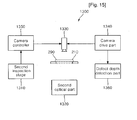
- FIG. 15 is a schematic view of an apparatus for detecting defects in a wafer in accordance with still another exemplary embodiment of the present invention.
- an apparatus 1300 for detecting defects in a wafer in accordance with the present invention includes a second inspection stage 1310, a second optical part 1320, an area camera 1330, a camera drive part 1340, a camera controller 1350, and a defect depth detection part 1360.
- the wafer defect detection apparatus 1300 shown in FIG. 13 may be integrated with the wafer defect detection apparatus 200 or 1100 shown in FIG. 2 or 11 as a single apparatus.
- the second inspection stage 1310 provides an inspection region for disposing a wafer, defect positions of which are determined by the defect detection part 260, and the inspection region is formed of a transmissive material.
- the second optical part 1320 is disposed under the second inspection stage 1310 to radiate infrared light onto the wafer disposed on the second inspection stage 1310.
- the light source of the optical part 220 shown in FIG. 2 may be used as a light source of the second optical part 1320.
- the second optical part 1320 may be comprised of a beam splitter disposed on an optical path of the optical part 220 to diverge light, and a reflecting mirror for changing the optical path of the light diverged by the beam splitter to radiate the light onto the inspection region of the second inspection stage 1310.
- optical part shown in FIGS. 5 and 6 may also be used as the light source of the second optical part 1320.
- an optical splitter is installed at an intermediate part of the optical transmission path 520 to split light emitted from a light source 510 into the second optical part 1320.
- the area camera 1330 detects infrared light transmitted through the wafer disposed on the second inspection stage 1310 to output an obtained image signal.
- the camera drive part 1340 moves the area camera 1330 such that a focus of the area camera 1330 is formed at the position of the defect on the wafer disposed on the second inspection stage 1310, is driven from one surface of the wafer disposed on the second inspection stage 1310 to the other surface thereof in a direction perpendicular to the surface of the wafer, and outputs a pulse signal having a predetermined period corresponding to a straight moving distance of the area camera 1330.
- a vertical moving distance of the area camera 1330 is also 700 ⁇ m.
- the camera controller 1350 counts the pulse signal input from the camera drive part 1340, and outputs a photographing instruction signal for controlling the area camera 1330 to photograph the wafer disposed on the second inspection stage 1310 whenever a pre-set number of pulse signals is input.
- the defect depth detection part 1360 detects the depth of the defect in the wafer disposed on the second inspection stage 1310 on the basis of the counted number of accumulated pulse signals at the time when a photographing instruction signal corresponding to an image signal having the clearest defect region among the image signals photographed by the area camera 1330 according to the photographing instruction signal input from the camera controller 1350 is output.
- the camera drive part 1340 is set to output a pulse whenever the area camera 1330 moves by 0.1 nm in a direction from a lower surface of the wafer to an upper surface thereof, when the counted number of pulse signals accumulated at the time of the output of the photographing instruction signal corresponding to the image signal having the clearest defect region is 100, the depth of the defect is 10nm from the lower surface of the wafer.
- FIG. 16 is a flowchart showing a method of detecting defects in a wafer in accordance with an example.
- a wafer 290 to be inspected is disposed in an inspection region formed of a transmissive material on an inspection stage 210 (S1400). Then, a conveyer part 240 conveys an image obtaining part 230 including a plurality of line sensors having striped photographing regions or an inspection stage 210 in a short-side direction of the photographing region of the line sensor; and outputs a pulse signal having a predetermined period corresponding to a relative straight moving distance between the image obtaining part 230 and the inspection stage 210 (S1410).
- a controller 250 counts the pulse signal and outputs a photographing instruction signal to the image obtaining part 230 whenever the wafer 290 is conveyed toward the image obtaining part 230 by a distance corresponding to the length of a short side of the photographing region in a short-side direction of the photographing region of the line sensor (S1420).
- Each of the line sensors installed at the image obtaining part 230 transmits charges accumulated therein to the line sensor adjacent in the opposite direction of the conveyance direction when the photographing instruction signal is input, and then detects infrared light transmitted through the wafer 290 disposed on the inspection stage 210.
- the line sensor disposed at an end in an opposite direction of the conveyance direction outputs the charges accumulated therein as an image signal from the time when the number of input photographing instruction signals exceeds the number of line sensors (S1430).
- a defect detection part 260 combines the image signals to generate an inspection image corresponding to the wafer 290 (S1440). Next, the defect detection part 260 determines the region in which an absolute value of the difference between a grey scale value of pixels constituting the generated inspection image and a pre-set reference grey scale value is larger than a predetermined reference value, as a defect region, and outputs positions and sizes of the defect region (S1450).
- FIG. 17 is a flowchart showing a method of detecting defects in a wafer in accordance with another example.
- the method of detecting defects in a wafer shown in FIG. 17 may be performed sequentially after the method of detecting defects in a wafer described with reference to FIG. 14 on the basis of the results of the method of FIG. 16 .
- a wafer, defect positions of which are determined is conveyed onto an inspection region formed of a transmissive material on the second inspection stage 1310 (S1500).
- a camera drive part 1340 moves an area camera 1330 such that a focus of the area camera 1330 is formed at the position of the defect in the wafer disposed on the second inspection stage 1310, is driven from one surface of the wafer disposed on the lower inspection stage 1310 to the other surface thereof in a direction perpendicular to the surface of the wafer, and outputs a pulse signal having a predetermined period corresponding to a straight moving distance of the area camera 1330 (S1510).
- a camera controller 1350 counts a pulse signal, detects infrared light radiated from a second optical part 1320 disposed under the second inspection stage 1310 and transmitted through the wafer disposed on the second inspection stage 1310 using the area camera 1330 whenever a pre-set number of pulse signals in input, and then obtains an image signal (S1520).
- a defect depth detection part 1360 detects the depth of a defect in the wafer disposed on the second inspection stage 1310 on the basis of the counted number of pulse signals accumulated at the time when a photographing instruction signal corresponding to an image signal having the clearest defect region among the image signals photographed by the area camera 1330 is output (S1530).
- An apparatus and method for detecting defects in a wafer in accordance with the present invention is capable of scanning infrared light transmitted through a wafer using line sensors, and accumulating signals obtained by the line sensors to rapidly detect defects from a generated inspection image, thereby ensuring operational compatibility with other apparatuses used in a wafer manufacturing process and enabling practical use of the apparatus.
- infrared light intensity can be minimized by enhancing the uniformity of the light using a fly-eye lens, it is possible to employ a low-power infrared light source.
- a light source mounting part can be movably installed to readily adjust light uniformity when light intensity is reduced as a result of changing the light source or lapse of time.
- the present invention may also be implemented as a computer code stored in a computer-readable recording medium.
- the computer-readable recording medium includes all kinds of recording devices in which computer data is stored, for example, a read only memory (ROM), a random access memory (RAM), a compact disc read only memory (CD ROM), a magnetic tape, a floppy disc, an optical data storage device, and carrier waves (for example, transmission through the Internet). Further, the computer-readable recording medium may be distributed among computer systems connected via a network such that the computer code can be stored and executed in a decentralized manner.
Landscapes
- Engineering & Computer Science (AREA)
- Physics & Mathematics (AREA)
- General Physics & Mathematics (AREA)
- Health & Medical Sciences (AREA)
- Toxicology (AREA)
- Chemical & Material Sciences (AREA)
- Microelectronics & Electronic Packaging (AREA)
- Theoretical Computer Science (AREA)
- Computer Vision & Pattern Recognition (AREA)
- Electromagnetism (AREA)
- Multimedia (AREA)
- General Engineering & Computer Science (AREA)
- Life Sciences & Earth Sciences (AREA)
- Computer Hardware Design (AREA)
- Analytical Chemistry (AREA)
- Biochemistry (AREA)
- General Health & Medical Sciences (AREA)
- Immunology (AREA)
- Pathology (AREA)
- Investigating Materials By The Use Of Optical Means Adapted For Particular Applications (AREA)
- Testing Or Measuring Of Semiconductors Or The Like (AREA)
Claims (18)
- Vorrichtung (200) zum Erfassen von Defekten in einem Wafer, umfassend:eine Inspektionsstufe (210), die einen Inspektionsbereich aufweist, auf welchem ein zu inspizierender Wafer angeordnet ist, der aus einem durchlässigen Material gebildet ist;ein optisches Bauteil (220), das unter der Inspektionsstufe angeordnet ist und Infrarotlicht auf den zu inspizierenden Wafer strahlt;ein Bilderhaltungsbauteil (230), das aus einer Mehrzahl von Zeilensensoren (S1 bis S4) gebildet ist, die jeweils einen gestreiften Photographierbereich aufweisen, und das Infrarotlicht erfasst, das durch den auf der Inspektionsstufe angeordneten Wafer übertragen wurde, um ein Bildsignal auszugeben;ein Förderbauteil (240) zum Fördern des Bilderhaltungsbauteils oder der Inspektionsstufe in einer Richtung der kurzen Seite des Photographierbereichs des Zeilensensors und Ausgeben eines Impulssignals mit einer vorbestimmten Periode, das einer relativ geraden Bewegungsstrecke zwischen dem Bilderhaltungsbauteil und der Inspektionsstufe entspricht;eine Steuerung (250) zum Zählen des Impulssignals und Steuern des Bilderhaltungsbauteils, um den Wafer zu photographieren, wann immer der Wafer in der Richtung der kurzen Seite des Photographierbereichs des Zeilensensors zu dem Bilderhaltungsbauteil um eine Strecke befördert wird, der der Länge der kurzen Seite des Photographierbereichs entspricht; undein Defekterfassungsbauteil (260) zum Kombinieren jedes von dem Bilderhaltungsbauteil ausgegebenen Bildsignals, um ein dem Wafer entsprechendes Inspektionsbild zu erzeugen, und Erfassen von Positionen von in dem Wafer existierenden Defekten aus dem Inspektionsbild,wobei jeder der Zeilensensoren darin akkumulierte Ladungen an einen benachbarten Zeilensensor in einer entgegengesetzten Richtung der Förderrichtung überträgt, wenn ein Photographier-Anweisungssignal von der Steuerung eingegeben wird, und dann das Infrarotlicht erfasst, das durch den auf der Inspektionsstufe angeordneten Wafer übertragen wird, und der Zeilensensor, der an einem Ende in einer entgegengesetzten Richtung der Förderrichtung positioniert ist, darin akkumulierte Ladungen als das Bildsignal zu einem Zeitpunkt ausgibt, wenn die Anzahl eingegebener Photographiersignale die Anzahl von Zeilensensoren überschreitet,dadurch gekennzeichnet, dass das optische Bauteil umfasst:eine Infrarotlampe (310) zum Emittieren des Infrarotlichts; undeine Positionierstufe (330), die eine darin angebrachte Infrarotlampe aufweist und in drei axialen Richtungen bewegbar ist, die ein orthogonales Koordinatensystem bilden;ein optischesGleichmäßigkeits-Einstellbauteil (380) zum Erfassen einer Mehrzahl von Teilbildern zum Einstellen der optischen Gleichmäßigkeit aus einem Inspektionsbild einer Probe eines Wafers, der keinen Defekt aufweist, und Treiben der Positionierstufe, um eine Position der Infrarotlampe zu ändern, entweder wenn eine Differenz zwischen dem höchsten und dem niedrigsten der von den Teilbildern gemessenen Graustufenwerte größer als ein vorbestimmter Referenzwert ist, oder wenn die höchste der Differenzen zwischen einem Mittelwert der von den Teilbildern gemessenen Graustufenwerte und den Graustufenwerte größer als ein vorbestimmter Referenzwert ist.
- Vorrichtung zum Erfassen von Defekten in einem Wafer gemäß Anspruch 1, bei der das Defekterfassungsbauteil (260) umfasst:ein Inspektionsbild-Erzeugungsbauteil (262) zum Kombinieren der Bildsignale, um ein Inspektionsbild zu erzeugen, das dem zu inspizierenden Wafer entspricht; undein Defektbestimmungsbauteil (264) zum Bestimmen eines aus Pixeln zusammengesetzten Bereichs, in welchem ein Absolutwert einer Differenz zwischen Graustufenwerten von Pixeln, die das erzeugte Inspektionsbild bilden, und einem voreingestellten Referenzgraustufenwert größer als ein vorbestimmter Referenzwert ist, als einen Defektbereich und Ausgeben der Position und Größe des Defektbereichs.
- Vorrichtung zum Erfassen von Defekten in einem Wafer gemäß Anspruch 2, bei der das Defektbestimmungsbauteil (264) einen Defektbereich, der einen Durchmesser größer als einen vorbestimmten Referenzdurchmesser aufweist, unter den Defektbereichen als einen in dem Wafer existierenden Defekt erfasst.
- Vorrichtung zum Erfassen von Defekten in einem Wafer gemäß Anspruch 1, bei der das optische Bauteil umfasst:eine Infrarotlampe (310) zum Emittieren von Infrarotlicht;einen optischen Übertragungsweg (530) zum Übertragen des von der Infrarotlampe emittierten Infrarotlichts; undein lineares Lichtleitelement (530) zum Umwandeln des durch den optischen Übertragungsweg übertragenen Infrarotlichts in lineares Licht.
- Vorrichtung zum Erfassen von Defekten in einem Wafer gemäß Anspruch 4, bei der das Defekterfassungsbauteil umfasst:ein Inspektionsbild-Erzeugungsbauteil (262) zum Kombinieren der Bildsignale, um ein dem zu inspizierenden Wafer entsprechendes Inspektionsbild zu erzeugen; undein Defektbestimmungsbauteil (264) zum Bestimmen eines aus Pixeln zusammengesetzten Bereichs, in welchem ein Absolutwert einer Differenz zwischen Graustufenwerten von Pixeln, die das erzeugte Inspektionsbild bilden, und einem voreingestellten Referenzgraustufenwert größer als ein vorbestimmter Referenzwert ist, als einen Defektbereich und Ausgeben der Position und Größe des Defektbereichs.
- Vorrichtung zum Erfassen von Defekten in einem Wafer gemäß Anspruch 5, bei der das Defektbestimmungsbauteil (264) einen Defektbereich, der einen Durchmesser aufweist, der größer als ein vorbestimmter Referenzdurchmesser ist, unter den Defektbereichen als einen in dem Wafer existierenden Defekt erfasst.
- Vorrichtung zum Erfassen von Defekten in einem Wafer gemäß Anspruch 1, ferner umfassend:ein Wafer-Förderbauteil (1110) zum Extrahieren des Wafers aus einer Vorratskassette, in welcher Wafer angebracht sind, um den Wafer zu dem Inspektionsbereich zu fördern, und Entfernen des Wafers von dem Inspektionsbereich, wenn die Defektinspektion durch das Defekterfassungsbauteil abgeschlossen ist;eine erste Kassette (1120) zum Aufnehmen des Wafers, der Defekte darin unter den Wafern aufweist; undeine zweite Kassette (1130) zum Aufnehmen des Wafers, der keinen Defekt unter den Wafern aufweist.
- Vorrichtung zum Erfassen von Defekten in einem Wafer gemäß Anspruch 7, ferner umfassend:ein optisches Zeichenlesebauteil (1150) zum Lesen von dem Wafer gegebener inhärenter Kennzeichnungsinformation von dem Wafer; undein Erfassungsergebnis-Speicherbauteil (1160) zum Speichern des Defekterfassungsergebnisses durch das Defekterfassungsbauteil auf der Grundlage der von dem Wafer gelesenen Kennzeichnungsinformation.
- Vorrichtung zum Erfassen von Defekten in einem Wafer gemäß Anspruch 1, ferner umfassend:eine zweite Inspektionsstufe (1310), die einen Inspektionsbereich aufweist, auf der ein Wafer mit der durch das Defekterfassungsbauteil erfassten Defektposition angeordnet ist, der aus einem durchlässigen Material gebildet ist;ein zweites optisches Bauteil (1320), das unter der zweiten Inspektionsstufe angeordnet ist und Infrarotlicht auf den auf der zweiten Inspektionsstufe angeordneten Wafer strahlt;eine Flächenkamera (1330) zum Ausgeben eines zweiten Bildsignals, das durch Erfassen von Infrarotlicht erhalten wird, das durch den auf der zweiten Inspektionsstufe angeordneten Wafer übertragen wird;ein Kameraantriebsbauteil (1340) zum Bewegen der Flächenkamera, so dass ein Brennpunkt der Flächenkamera an einer Position des Defekts gebildet wird, der in dem auf der zweiten Inspektionsstufe angeordneten Wafer existiert, wobei von einer Oberfläche des auf der zweiten Inspektionsstufe angeordneten Wafers zu der anderen Oberfläche desselben in einer Richtung senkrecht zu der Oberfläche des Wafers angetrieben wird, und Ausgeben eines Impulssignals mit einer vorbestimmten Periode, das einer geraden Bewegungsstrecke der Flächenkamera entspricht;eine Kamerasteuerung (1350) zum Zählen eines von dem Kameraantriebsbauteil eingegebenen Impulssignals und Ausgeben eines Photographier-Anweisungssignals, das die Flächenkamera steuert, um den auf der zweiten Inspektionsstufe angeordneten Wafer zu photographieren, wann immer eine voreingestellte Anzahl von Impulssignalen eingegeben wird; undein Defekttiefen-Erfassungsbauteil (1360) zum Erfassen einer Tiefe des Defekts, der in dem auf der zweiten Inspektionsstufe angeordneten Wafer existiert, auf der Grundlage der gezählten Anzahl von akkumulierten Impulssignalen zu dem Zeitpunkt, wenn ein PhotographierAnweisungssignal, das einem Bildsignal mit einem deutlichsten Defektbereich unter den durch die Flächenkamera gemäß dem Photographier-Anweisungssignal photographierten zweiten Bildsignalen entspricht, ausgegeben wird.
- Vorrichtung zum Erfassen von Defekten in einem Wafer gemäß Anspruch 9, bei der das Defekterfassungsbauteil (1360) umfasst:ein Inspektionsbild-Erzeugungsbauteil zum Kombinieren der Bildsignale, um ein dem Wafer entsprechendes Inspektionsbild zu erzeugen; undein Defektbestimmungsbauteil zum Bestimmen eines aus Pixeln zusammengesetzten Bereichs, in welchem ein Absolutwert einer Differenz zwischen Graustufenwerten von Pixeln, die das erzeugte Inspektionsbild bilden, und einem voreingestellten Referenzgraustufenwert größer als ein vorbestimmter Referenzwert ist, als einen Defektbereich und Ausgeben der Position und Größe des Defektbereichs.
- Vorrichtung zum Erfassen von Defekten in einem Wafer gemäß Anspruch 1, bei der das von dem optischen Bauteil ausgestrahlte Infrarotlicht eine Wellenlänge von 750 nm bis 850 nm aufweist.
- Verfahren zum Erfassen von Defekten in einem Wafer (290), das die folgenden Schritte umfasst:(a) Positionieren eines zu prüfenden Wafers (290) in einem Inspektionsbereich auf einer Inspektionsstufe (210), wobei der Inspektionsbereich aus einem durchlässigen Material gebildet ist;(b) Fördern einer Bilderhaltungsvorrichtung, die eine Mehrzahl von Zeilensensoren (S1 bis S4) mit jeweils einem gestreiften Photographierbereich aufweist, oder der Inspektionsstufe in einer Richtung der kurzen Seite eines Photographierbereichs des Zeilensensors und Ausgeben eines Impulssignals mit einer vorbestimmten Periode, das einer relativ geraden Bewegungsstrecke zwischen der Bilderhaltungsvorrichtung und der Inspektionsstufe entspricht;(c) Zählen des Impulssignals und Ausgeben eines Photographier-Anweisungssignals an die Bilderhaltungsvorrichtung, wann immer der Wafer in der Richtung der kurzen Seite des Photographierbereichs des Zeilensensors zu der Bilderhaltungsvorrichtung hin um eine Strecke gefördert wird, die der Länge der kurzen Seite des Photographierbereichs entspricht;(d) Erfassen von Infrarotlicht, das von einer unter der Inspektionsstufe angeordneten Lichtquelle ausgestrahlt wird und durch den Wafer übertragen wird, unter Verwendung der Bilderhaltungsvorrichtung und Ausgeben eines Bildsignals; und(e) Kombinieren der Bildsignale, um ein dem Wafer entsprechendes Inspektionsbild zu erzeugen, und Erfassen der Positionen von in dem Wafer existierenden Defekten aus dem erzeugten Inspektionsbild,
wobei jeder der Zeilensensoren darin akkumulierte Ladungen an einen benachbarten Zeilensensor in einer entgegengesetzten Richtung der Förderrichtungüberträgt, wenn ein Photographier-Anweisungssignal eingegeben wird, und dann das Infrarotlichterfasst, das durch den auf der Inspektionsstufe angeordneten Wafer übertragen wird, und der Zeilensensor, der an einem Ende in einer entgegengesetzten Richtung der Förderrichtung positioniert ist, darin akkumulierte Ladungen als das Bildsignal zu einem Zeitpunkt ausgibt, wenn die Anzahl eingegebener Photographiersignale die Anzahl von Zeilensensoren überschreitet,
dadurch gekennzeichnet, dass das Verfahren zum Erfassen von Defekten in einem Wafer ferner umfasst:(f) Erfassen einer Mehrzahl von Teilbildern zum Einstellen von optischer Gleichmäßigkeit aus einem Inspektionsbild einer Probe eines Wafers, der keinen Defekt aufweist, und(g) Treiben einer Positionierstufe (330), die in drei axialen Richtungen bewegbar ist, die ein orthogonales Koordinatensystem bilden, um eine Position der Lichtquelle zu ändern, entweder wenn eine Differenz zwischen dem höchsten und dem niedrigsten der Graustufenwerte, die von den Teilbildern gemessen wurden, einen vorbestimmten Referenzwert überschreitet, oder wenn die höchste der Differenzen zwischen einem Mittelwert von Graustufenwerten, die von den Teilbildern gemessen wurden, und den Graustufenwerten einen vorbestimmten Referenzwert überschreitet. - Verfahren zum Erfassen von Defekten in einem Wafer gemäß Anspruch 12, bei dem Schritt (e) umfasst:(e1) Kombinieren der Bildsignale, um ein dem Wafer entsprechendes Inspektionsbild zu erzeugen; und(e2) Bestimmen eines aus Pixeln zusammengesetzten Bereichs, in welchem ein Absolutwert einer Differenz zwischen Graustufenwerten von Pixeln, die das erzeugte Inspektionsbild bilden, und einem voreingestellten Referenzgraustufenwert größer als ein vorbestimmter Referenzwert ist, als einen Defektbereich und Ausgeben der Position und Größe des Defektbereichs.
- Verfahren zum Erfassen von Defekten in einem Wafer (290) gemäß Anspruch 13, bei dem in Schritt (e2) ein Defektbereich, der einen Durchmesser aufweist, der größer als ein vorbestimmter Referenzdurchmesser ist, unter den Defektbereichen als ein in dem Wafer existierender Defekt erfasst wird.
- Verfahren zum Erfassen von Defekten in einem Wafer (290) gemäß Anspruch 12, ferner umfassend:Lesen der dem Wafer gegebenen inhärenten Kennzeichnungsinformation aus dem Wafer vor Schritt (a); undSpeichern des Defekterfassungsergebnisses des Wafers auf der Grundlage der aus dem Wafer gelesenen Kennzeichnungsinformation nach Schritt (e).
- Verfahren zum Erfassen von Defekten in einem Wafer (290) gemäß Anspruch 12, das ferner die folgenden Schritte umfasst:(h) Fördern des Wafers, wobei eine Defektposition desselben erkannt wird, auf einen Inspektionsbereich, der aus einem durchlässigen Material auf einer zweiten Inspektionsstufe (1310) ausgebildet ist;(i) Bewegen einer Flächenkamera (1330), so dass ein Brennpunkt der Flächenkamera an einer Position des Defekts gebildet wird, der in dem auf der zweiten Inspektionsstufe angeordneten Wafer existiert, Treiben der Flächenkamera von einer Oberfläche des auf der zweiten Inspektionsstufe angeordneten Wafers zu der anderen Oberfläche desselben in einer Richtung senkrecht zu der Oberfläche des Wafers und Ausgeben eines Impulssignals mit einer vorbestimmten Periode, das einer geraden Bewegungstrecke der Flächenkamera entspricht;(j) Zählen des Impulssignals und Erfassen von Infrarotlicht, das von einer unter der zweiten Inspektionsstufe angeordneten zweiten Lichtquelle ausgestrahlt und durch den auf der zweiten Inspektionsstufe angeordneten Wafer übertragen wird, unter Verwendung der Flächenkamera, wann immer eine voreingestellte Anzahl von Impulssignalen eingegeben wird, um ein zweites Bildsignal zu erhalten; und(k) Erfassen einer Tiefe des Defekts, der in dem auf der zweiten Inspektionsstufe angeordneten Wafer existiert, auf der Grundlage der gezählten Anzahl von akkumulierten Impulssignalen zu dem Zeitpunkt, wenn ein Photographier-Anweisungssignal, das einem Bildsignal mit einem deutlichsten Defektbereich unter den durch die Flächenkamera photographierten zweiten Bildsignalen entspricht, ausgegeben wird.
- Verfahren zum Erfassen von Defekten in einem Wafer gemäß Anspruch 16, bei dem Schritt (e) umfasst:(e1) Kombinieren der Bildsignale, um ein dem Wafer entsprechendes Inspektionsbild zu erzeugen; und(e2) Bestimmen eines aus Pixeln zusammengesetzten Bereichs, in welchem ein Absolutwert einer Differenz zwischen Graustufenwerten von Pixeln, die das erzeugte Inspektionsbild bilden, und einem voreingestellten Referenzgraustufenwert größer als ein vorbestimmter Referenzwert ist, als einen Defektbereich und Ausgeben der Position und Größe des Defektbereichs.
- Verfahren zum Erfassen von Defekten in einem Wafer (290) gemäß einem der Ansprüche 12, 16 oder 17, bei dem das von der Lichtquelle ausgestrahlte Infrarotlicht eine Wellenlänge von 750 nm bis 850 nm aufweist.
Applications Claiming Priority (2)
| Application Number | Priority Date | Filing Date | Title |
|---|---|---|---|
| KR20060011840 | 2006-02-07 | ||
| PCT/KR2007/000673 WO2007091846A1 (en) | 2006-02-07 | 2007-02-07 | Apparatus and method for detecting defects in wafer using line sensor camera |
Publications (3)
| Publication Number | Publication Date |
|---|---|
| EP1997134A1 EP1997134A1 (de) | 2008-12-03 |
| EP1997134A4 EP1997134A4 (de) | 2012-10-31 |
| EP1997134B1 true EP1997134B1 (de) | 2014-07-23 |
Family
ID=38345395
Family Applications (1)
| Application Number | Title | Priority Date | Filing Date |
|---|---|---|---|
| EP07708823.5A Not-in-force EP1997134B1 (de) | 2006-02-07 | 2007-02-07 | Vorrichtung und verfahren zum detektieren von defekten in einem wafer unter verwendung einer zeilensensorkamera |
Country Status (6)
| Country | Link |
|---|---|
| US (1) | US8055058B2 (de) |
| EP (1) | EP1997134B1 (de) |
| KR (1) | KR100793182B1 (de) |
| MY (1) | MY143415A (de) |
| TW (1) | TWI314988B (de) |
| WO (1) | WO2007091846A1 (de) |
Families Citing this family (40)
| Publication number | Priority date | Publication date | Assignee | Title |
|---|---|---|---|---|
| JP4333762B2 (ja) * | 2007-03-23 | 2009-09-16 | 株式会社デンソー | 燃料噴射弁を箱詰めする方法 |
| TWI427271B (zh) * | 2008-11-14 | 2014-02-21 | Hon Hai Prec Ind Co Ltd | 光照調節方法及其電腦系統 |
| DE102009050711A1 (de) | 2009-10-26 | 2011-05-05 | Schott Ag | Verfahren und Vorrichtung zur Detektion von Rissen in Halbleitersubstraten |
| WO2011102622A2 (ko) * | 2010-02-17 | 2011-08-25 | 한미반도체 주식회사 | 잉곳 검사 장치 및 방법 |
| KR101157081B1 (ko) | 2010-04-28 | 2012-07-03 | 주식회사 에이치앤씨 | 조명장치와 이를 포함하는 기판 검사 장치 |
| KR101214806B1 (ko) * | 2010-05-11 | 2012-12-24 | 가부시키가이샤 사무코 | 웨이퍼 결함 검사 장치 및 웨이퍼 결함 검사 방법 |
| JP6004517B2 (ja) * | 2011-04-19 | 2016-10-12 | 芝浦メカトロニクス株式会社 | 基板検査装置、基板検査方法及び該基板検査装置の調整方法 |
| CN102435629B (zh) * | 2011-11-28 | 2015-01-21 | 上海华力微电子有限公司 | 扫描电子显微镜的检测方法 |
| US8948494B2 (en) * | 2012-11-12 | 2015-02-03 | Kla-Tencor Corp. | Unbiased wafer defect samples |
| TW201511152A (zh) * | 2013-09-09 | 2015-03-16 | Cheng Mei Instr Technology Co Ltd | 線性掃瞄總成 |
| US9747520B2 (en) * | 2015-03-16 | 2017-08-29 | Kla-Tencor Corporation | Systems and methods for enhancing inspection sensitivity of an inspection tool |
| US10402671B2 (en) * | 2016-03-28 | 2019-09-03 | General Dynamics Mission Systems, Inc. | System and methods for automatic solar panel recognition and defect detection using infrared imaging |
| CN106841224A (zh) * | 2017-04-17 | 2017-06-13 | 江南大学 | 一种纱线图像定距触发采集系统 |
| US20190015662A1 (en) | 2017-07-12 | 2019-01-17 | Milind Chandrakant Raje | Monolithic component for an implantable medical device |
| CN109884077A (zh) * | 2017-12-06 | 2019-06-14 | 上海太阳能工程技术研究中心有限公司 | 自然光环境下的户外光伏电站的红外缺陷检测方法及装置 |
| CN108648168A (zh) * | 2018-03-15 | 2018-10-12 | 北京京仪仪器仪表研究总院有限公司 | Ic晶圆表面缺陷检测方法 |
| US11056366B2 (en) * | 2018-03-23 | 2021-07-06 | Kla Corporation | Sample transport device with integrated metrology |
| CN108613916A (zh) * | 2018-07-03 | 2018-10-02 | 深圳市智信精密仪器有限公司 | 一种用于金刚砂检测的测量设备及其测量方法 |
| KR20200046967A (ko) | 2018-10-26 | 2020-05-07 | 삼성에스디에스 주식회사 | 결함 검출 장치 및 방법 |
| US11300525B2 (en) * | 2019-07-31 | 2022-04-12 | Taiwan Semiconductor Manufacturing Company, Ltd. | Wafer inspection apparatus and method |
| CN111060528B (zh) * | 2019-12-31 | 2023-02-07 | 塔里木大学 | 水果缺陷发展规律光学检测系统及检测方法 |
| JP7563898B2 (ja) * | 2020-05-26 | 2024-10-08 | 株式会社ディスコ | 透明部材又は半透明部材を貼り合わせた貼り合わせワークの研削方法、及び貼り合わせワークの研削装置 |
| CN112097824A (zh) * | 2020-07-31 | 2020-12-18 | 芜湖桑乐金电子科技有限公司 | 一种碳晶发热板检测装置 |
| US11651981B2 (en) * | 2020-08-18 | 2023-05-16 | Taiwan Semiconductor Manufacturing Co., Ltd. | Method and system for map-free inspection of semiconductor devices |
| KR102635249B1 (ko) * | 2020-08-31 | 2024-02-08 | 세메스 주식회사 | 이미지 획득 방법, 이미지 획득 장치 및 웨이퍼 검사 장치 |
| CN114723650A (zh) * | 2020-12-21 | 2022-07-08 | 东方晶源微电子科技(北京)有限公司 | 晶圆缺陷检测方法和装置、设备及存储介质 |
| CN114923910A (zh) * | 2021-02-03 | 2022-08-19 | 京东科技信息技术有限公司 | 缺陷检测装置、巡检设备、缺陷检测方法 |
| JP7573939B2 (ja) * | 2021-02-19 | 2024-10-28 | 株式会社ディスコ | 検出装置 |
| CN113176223A (zh) * | 2021-03-23 | 2021-07-27 | 中山大学新华学院 | 一种红外分光光度检测仪 |
| CN113674273B (zh) * | 2021-09-16 | 2021-12-31 | 深圳市光明顶照明科技有限公司 | 一种基于产品缺陷的光学检测方法、系统和可读存储介质 |
| CN114354616A (zh) * | 2021-12-03 | 2022-04-15 | 东莞市瑞图新智科技有限公司 | 一种cis芯片缺陷检测方法及装置 |
| CN114724981B (zh) * | 2022-03-10 | 2023-02-28 | 江苏亚电科技有限公司 | 一种晶圆片数片装置及数片方法 |
| CN115356259A (zh) * | 2022-07-08 | 2022-11-18 | 维库(厦门)信息技术有限公司 | 一种基于深度学习的方形电容缺陷检测系统及方法 |
| US20240274401A1 (en) * | 2023-02-14 | 2024-08-15 | Kla Corporation | Substrate position monitoring devices |
| KR102810436B1 (ko) | 2023-04-10 | 2025-05-23 | 주식회사 넥서스원 | 반도체 웨이퍼 검사 장치 |
| KR102810434B1 (ko) | 2023-04-10 | 2025-05-23 | 주식회사 넥서스원 | 반도체 웨이퍼 검사 방법 |
| CN117078667B (zh) * | 2023-10-13 | 2024-01-09 | 山东克莱蒙特新材料科技有限公司 | 基于机器视觉的矿物铸件检测方法 |
| CN117269197B (zh) * | 2023-11-21 | 2024-02-02 | 昆明理工大学 | 多晶硅原料表面质量检测方法及检测装置 |
| CN117636698B (zh) * | 2023-12-28 | 2024-06-07 | 北京奥康达体育科技有限公司 | 一种学生考试用数字化引体向上辅助训练系统 |
| US20250247512A1 (en) * | 2024-01-26 | 2025-07-31 | Robotic Research Opco, Llc | Stereo camera with frameless image sensing |
Family Cites Families (15)
| Publication number | Priority date | Publication date | Assignee | Title |
|---|---|---|---|---|
| DE3578768D1 (de) * | 1985-03-14 | 1990-08-23 | Toppan Printing Co Ltd | Einrichtung zum ueberpruefen von abdruecken. |
| US5153444A (en) * | 1988-12-23 | 1992-10-06 | Hitachi, Ltd. | Method and apparatus for detecting patterns |
| KR960007481B1 (ko) * | 1991-05-27 | 1996-06-03 | 가부시끼가이샤 히다찌세이사꾸쇼 | 패턴검사방법 및 장치 |
| JP3229411B2 (ja) | 1993-01-11 | 2001-11-19 | 株式会社日立製作所 | 薄膜トランジスタ基板の欠陥検出方法およびその修正方法 |
| JP3298250B2 (ja) * | 1993-07-30 | 2002-07-02 | ソニー株式会社 | 自動検査方法及び自動検査装置 |
| US5981949A (en) * | 1996-01-18 | 1999-11-09 | The United States Of America As Represented By The Secretary Of The Air Force | Locating defects in solid material |
| US6091075A (en) * | 1997-06-04 | 2000-07-18 | Hitachi, Ltd. | Automatic focus detection method, automatic focus detection apparatus, and inspection apparatus |
| JP3397101B2 (ja) * | 1997-10-29 | 2003-04-14 | 株式会社日立製作所 | 欠陥検査方法および装置 |
| US6800859B1 (en) * | 1998-12-28 | 2004-10-05 | Hitachi, Ltd. | Method and equipment for detecting pattern defect |
| JP4481397B2 (ja) * | 1999-09-07 | 2010-06-16 | オリンパス株式会社 | 光学装置及び顕微鏡 |
| US7109464B2 (en) * | 2001-07-06 | 2006-09-19 | Palantyr Research, Llc | Semiconductor imaging system and related methodology |
| AU2002349599A1 (en) * | 2001-11-30 | 2003-06-10 | International Business Machines Corporation | Inspection device and inspection method for pattern profile, exposure system |
| JP3729154B2 (ja) * | 2002-05-10 | 2005-12-21 | 株式会社日立製作所 | パターン欠陥検査方法及びその装置 |
| JP3784762B2 (ja) | 2002-09-26 | 2006-06-14 | 株式会社日立国際電気 | パターン欠陥検査装置およびパターン欠陥検査方法 |
| DE102004015326A1 (de) * | 2004-03-30 | 2005-10-20 | Leica Microsystems | Vorrichtung und Verfahren zur Inspektion eines Halbleiterbauteils |
-
2007
- 2007-02-07 TW TW096104542A patent/TWI314988B/zh not_active IP Right Cessation
- 2007-02-07 KR KR1020070012924A patent/KR100793182B1/ko not_active Expired - Fee Related
- 2007-02-07 WO PCT/KR2007/000673 patent/WO2007091846A1/en not_active Ceased
- 2007-02-07 EP EP07708823.5A patent/EP1997134B1/de not_active Not-in-force
- 2007-02-07 US US12/296,134 patent/US8055058B2/en not_active Expired - Fee Related
- 2007-02-07 MY MYPI20083941A patent/MY143415A/en unknown
Also Published As
| Publication number | Publication date |
|---|---|
| WO2007091846A1 (en) | 2007-08-16 |
| US8055058B2 (en) | 2011-11-08 |
| MY143415A (en) | 2011-05-13 |
| US20090257646A1 (en) | 2009-10-15 |
| TWI314988B (en) | 2009-09-21 |
| KR20070080591A (ko) | 2007-08-10 |
| EP1997134A1 (de) | 2008-12-03 |
| EP1997134A4 (de) | 2012-10-31 |
| KR100793182B1 (ko) | 2008-01-10 |
| TW200732650A (en) | 2007-09-01 |
Similar Documents
| Publication | Publication Date | Title |
|---|---|---|
| US8055058B2 (en) | Apparatus and method for detecting defects in wafer using line sensor camera | |
| US10412311B2 (en) | Focus adjustment for surface part inspection | |
| KR101174081B1 (ko) | 평면 기판 자동 감지 시스템 및 방법 | |
| US7714996B2 (en) | Automatic inspection system for flat panel substrate | |
| US8451440B2 (en) | Apparatus for the optical inspection of wafers | |
| US6937754B1 (en) | Inspection equipment | |
| US9863889B2 (en) | System and method for inspecting a wafer | |
| US8204298B2 (en) | Focusing method and apparatus | |
| JP5276643B2 (ja) | 弱い光及び蛍光の光の用途において信号対ノイズ比、解像度、又は合焦品質を犠牲にすることなく検査速度を最適化するための方法 | |
| US20130277553A1 (en) | Method and apparatus for observing defects | |
| CN109841533B (zh) | 宽频晶圆缺陷侦测系统及宽频晶圆缺陷侦测方法 | |
| KR20190062189A (ko) | 기판 검사 장치 및 기판 검사 방법 | |
| TWI633295B (zh) | 物品的表面特徵偵測及檢查設備 | |
| US12405228B2 (en) | Inspection apparatus and inspection method | |
| KR20220156625A (ko) | 고감도 이미지-기반 반사계측 | |
| KR101653176B1 (ko) | 자동초점거리 조절 기능을 갖는 렌즈 검사장치 | |
| CN115427754B (zh) | 高灵敏度的基于影像的反射测量 | |
| KR20060066041A (ko) | 백라이트 유닛 검사 장치 | |
| JP2004212353A (ja) | 光学的検査装置 | |
| US7443500B2 (en) | Apparatus for scattered light inspection of optical elements | |
| JP2014228670A (ja) | 焦点位置調整方法および検査方法 | |
| WO2025216977A1 (en) | Focus position measurement while scanning | |
| CN117517342A (zh) | 一种光学检测系统和光学检测方法 | |
| KR20140048831A (ko) | 포린 표면 피처들과 네이티브 표면 피처들의 구별 |
Legal Events
| Date | Code | Title | Description |
|---|---|---|---|
| PUAI | Public reference made under article 153(3) epc to a published international application that has entered the european phase |
Free format text: ORIGINAL CODE: 0009012 |
|
| 17P | Request for examination filed |
Effective date: 20081002 |
|
| AK | Designated contracting states |
Kind code of ref document: A1 Designated state(s): AT BE BG CH CY CZ DE DK EE ES FI FR GB GR HU IE IS IT LI LT LU LV MC NL PL PT RO SE SI SK TR |
|
| RIN1 | Information on inventor provided before grant (corrected) |
Inventor name: KIM, JIN-SEOB Inventor name: HWANG, BYOUNG-MOON Inventor name: HAN, JONG-KYU Inventor name: MOON, U-SEOCK |
|
| R17P | Request for examination filed (corrected) |
Effective date: 20081002 |
|
| DAX | Request for extension of the european patent (deleted) | ||
| A4 | Supplementary search report drawn up and despatched |
Effective date: 20120928 |
|
| RIC1 | Information provided on ipc code assigned before grant |
Ipc: G01N 21/95 20060101ALI20120927BHEP Ipc: G06K 9/20 20060101ALI20120927BHEP Ipc: G01R 31/311 20060101ALI20120927BHEP Ipc: H01L 21/66 20060101AFI20120927BHEP |
|
| GRAP | Despatch of communication of intention to grant a patent |
Free format text: ORIGINAL CODE: EPIDOSNIGR1 |
|
| INTG | Intention to grant announced |
Effective date: 20140131 |
|
| RIC1 | Information provided on ipc code assigned before grant |
Ipc: G01N 21/95 20060101ALI20140117BHEP Ipc: G01R 31/311 20060101ALI20140117BHEP Ipc: G06K 9/20 20060101ALI20140117BHEP Ipc: H01L 21/66 20060101AFI20140117BHEP |
|
| GRAS | Grant fee paid |
Free format text: ORIGINAL CODE: EPIDOSNIGR3 |
|
| GRAA | (expected) grant |
Free format text: ORIGINAL CODE: 0009210 |
|
| RAP1 | Party data changed (applicant data changed or rights of an application transferred) |
Owner name: HANTECH CO., LTD |
|
| AK | Designated contracting states |
Kind code of ref document: B1 Designated state(s): AT BE BG CH CY CZ DE DK EE ES FI FR GB GR HU IE IS IT LI LT LU LV MC NL PL PT RO SE SI SK TR |
|
| REG | Reference to a national code |
Ref country code: GB Ref legal event code: FG4D |
|
| REG | Reference to a national code |
Ref country code: CH Ref legal event code: EP |
|
| REG | Reference to a national code |
Ref country code: IE Ref legal event code: FG4D |
|
| REG | Reference to a national code |
Ref country code: AT Ref legal event code: REF Ref document number: 679287 Country of ref document: AT Kind code of ref document: T Effective date: 20140815 |
|
| REG | Reference to a national code |
Ref country code: DE Ref legal event code: R096 Ref document number: 602007037757 Country of ref document: DE Effective date: 20140904 |
|
| REG | Reference to a national code |
Ref country code: AT Ref legal event code: MK05 Ref document number: 679287 Country of ref document: AT Kind code of ref document: T Effective date: 20140723 |
|
| REG | Reference to a national code |
Ref country code: NL Ref legal event code: VDEP Effective date: 20140723 |
|
| REG | Reference to a national code |
Ref country code: LT Ref legal event code: MG4D |
|
| PG25 | Lapsed in a contracting state [announced via postgrant information from national office to epo] |
Ref country code: BG Free format text: LAPSE BECAUSE OF FAILURE TO SUBMIT A TRANSLATION OF THE DESCRIPTION OR TO PAY THE FEE WITHIN THE PRESCRIBED TIME-LIMIT Effective date: 20141023 Ref country code: PT Free format text: LAPSE BECAUSE OF FAILURE TO SUBMIT A TRANSLATION OF THE DESCRIPTION OR TO PAY THE FEE WITHIN THE PRESCRIBED TIME-LIMIT Effective date: 20141124 Ref country code: ES Free format text: LAPSE BECAUSE OF FAILURE TO SUBMIT A TRANSLATION OF THE DESCRIPTION OR TO PAY THE FEE WITHIN THE PRESCRIBED TIME-LIMIT Effective date: 20140723 Ref country code: GR Free format text: LAPSE BECAUSE OF FAILURE TO SUBMIT A TRANSLATION OF THE DESCRIPTION OR TO PAY THE FEE WITHIN THE PRESCRIBED TIME-LIMIT Effective date: 20141024 Ref country code: SE Free format text: LAPSE BECAUSE OF FAILURE TO SUBMIT A TRANSLATION OF THE DESCRIPTION OR TO PAY THE FEE WITHIN THE PRESCRIBED TIME-LIMIT Effective date: 20140723 Ref country code: FI Free format text: LAPSE BECAUSE OF FAILURE TO SUBMIT A TRANSLATION OF THE DESCRIPTION OR TO PAY THE FEE WITHIN THE PRESCRIBED TIME-LIMIT Effective date: 20140723 Ref country code: LT Free format text: LAPSE BECAUSE OF FAILURE TO SUBMIT A TRANSLATION OF THE DESCRIPTION OR TO PAY THE FEE WITHIN THE PRESCRIBED TIME-LIMIT Effective date: 20140723 |
|
| PG25 | Lapsed in a contracting state [announced via postgrant information from national office to epo] |
Ref country code: CY Free format text: LAPSE BECAUSE OF FAILURE TO SUBMIT A TRANSLATION OF THE DESCRIPTION OR TO PAY THE FEE WITHIN THE PRESCRIBED TIME-LIMIT Effective date: 20140723 Ref country code: NL Free format text: LAPSE BECAUSE OF FAILURE TO SUBMIT A TRANSLATION OF THE DESCRIPTION OR TO PAY THE FEE WITHIN THE PRESCRIBED TIME-LIMIT Effective date: 20140723 Ref country code: PL Free format text: LAPSE BECAUSE OF FAILURE TO SUBMIT A TRANSLATION OF THE DESCRIPTION OR TO PAY THE FEE WITHIN THE PRESCRIBED TIME-LIMIT Effective date: 20140723 Ref country code: IS Free format text: LAPSE BECAUSE OF FAILURE TO SUBMIT A TRANSLATION OF THE DESCRIPTION OR TO PAY THE FEE WITHIN THE PRESCRIBED TIME-LIMIT Effective date: 20141123 Ref country code: LV Free format text: LAPSE BECAUSE OF FAILURE TO SUBMIT A TRANSLATION OF THE DESCRIPTION OR TO PAY THE FEE WITHIN THE PRESCRIBED TIME-LIMIT Effective date: 20140723 Ref country code: AT Free format text: LAPSE BECAUSE OF FAILURE TO SUBMIT A TRANSLATION OF THE DESCRIPTION OR TO PAY THE FEE WITHIN THE PRESCRIBED TIME-LIMIT Effective date: 20140723 |
|
| REG | Reference to a national code |
Ref country code: DE Ref legal event code: R097 Ref document number: 602007037757 Country of ref document: DE |
|
| PG25 | Lapsed in a contracting state [announced via postgrant information from national office to epo] |
Ref country code: RO Free format text: LAPSE BECAUSE OF FAILURE TO SUBMIT A TRANSLATION OF THE DESCRIPTION OR TO PAY THE FEE WITHIN THE PRESCRIBED TIME-LIMIT Effective date: 20140723 Ref country code: SK Free format text: LAPSE BECAUSE OF FAILURE TO SUBMIT A TRANSLATION OF THE DESCRIPTION OR TO PAY THE FEE WITHIN THE PRESCRIBED TIME-LIMIT Effective date: 20140723 Ref country code: EE Free format text: LAPSE BECAUSE OF FAILURE TO SUBMIT A TRANSLATION OF THE DESCRIPTION OR TO PAY THE FEE WITHIN THE PRESCRIBED TIME-LIMIT Effective date: 20140723 Ref country code: CZ Free format text: LAPSE BECAUSE OF FAILURE TO SUBMIT A TRANSLATION OF THE DESCRIPTION OR TO PAY THE FEE WITHIN THE PRESCRIBED TIME-LIMIT Effective date: 20140723 Ref country code: DK Free format text: LAPSE BECAUSE OF FAILURE TO SUBMIT A TRANSLATION OF THE DESCRIPTION OR TO PAY THE FEE WITHIN THE PRESCRIBED TIME-LIMIT Effective date: 20140723 |
|
| PLBE | No opposition filed within time limit |
Free format text: ORIGINAL CODE: 0009261 |
|
| STAA | Information on the status of an ep patent application or granted ep patent |
Free format text: STATUS: NO OPPOSITION FILED WITHIN TIME LIMIT |
|
| PG25 | Lapsed in a contracting state [announced via postgrant information from national office to epo] |
Ref country code: BE Free format text: LAPSE BECAUSE OF NON-PAYMENT OF DUE FEES Effective date: 20150228 |
|
| 26N | No opposition filed |
Effective date: 20150424 |
|
| PG25 | Lapsed in a contracting state [announced via postgrant information from national office to epo] |
Ref country code: LU Free format text: LAPSE BECAUSE OF FAILURE TO SUBMIT A TRANSLATION OF THE DESCRIPTION OR TO PAY THE FEE WITHIN THE PRESCRIBED TIME-LIMIT Effective date: 20150207 |
|
| REG | Reference to a national code |
Ref country code: CH Ref legal event code: PL |
|
| GBPC | Gb: european patent ceased through non-payment of renewal fee |
Effective date: 20150207 |
|
| PG25 | Lapsed in a contracting state [announced via postgrant information from national office to epo] |
Ref country code: MC Free format text: LAPSE BECAUSE OF FAILURE TO SUBMIT A TRANSLATION OF THE DESCRIPTION OR TO PAY THE FEE WITHIN THE PRESCRIBED TIME-LIMIT Effective date: 20140723 Ref country code: CH Free format text: LAPSE BECAUSE OF NON-PAYMENT OF DUE FEES Effective date: 20150228 Ref country code: LI Free format text: LAPSE BECAUSE OF NON-PAYMENT OF DUE FEES Effective date: 20150228 |
|
| REG | Reference to a national code |
Ref country code: IE Ref legal event code: MM4A |
|
| REG | Reference to a national code |
Ref country code: FR Ref legal event code: ST Effective date: 20151030 |
|
| PG25 | Lapsed in a contracting state [announced via postgrant information from national office to epo] |
Ref country code: SI Free format text: LAPSE BECAUSE OF FAILURE TO SUBMIT A TRANSLATION OF THE DESCRIPTION OR TO PAY THE FEE WITHIN THE PRESCRIBED TIME-LIMIT Effective date: 20140723 |
|
| PG25 | Lapsed in a contracting state [announced via postgrant information from national office to epo] |
Ref country code: GB Free format text: LAPSE BECAUSE OF NON-PAYMENT OF DUE FEES Effective date: 20150207 Ref country code: IE Free format text: LAPSE BECAUSE OF NON-PAYMENT OF DUE FEES Effective date: 20150207 |
|
| PG25 | Lapsed in a contracting state [announced via postgrant information from national office to epo] |
Ref country code: FR Free format text: LAPSE BECAUSE OF NON-PAYMENT OF DUE FEES Effective date: 20150302 |
|
| PG25 | Lapsed in a contracting state [announced via postgrant information from national office to epo] |
Ref country code: BE Free format text: LAPSE BECAUSE OF FAILURE TO SUBMIT A TRANSLATION OF THE DESCRIPTION OR TO PAY THE FEE WITHIN THE PRESCRIBED TIME-LIMIT Effective date: 20140723 |
|
| PGFP | Annual fee paid to national office [announced via postgrant information from national office to epo] |
Ref country code: DE Payment date: 20170104 Year of fee payment: 11 |
|
| PG25 | Lapsed in a contracting state [announced via postgrant information from national office to epo] |
Ref country code: HU Free format text: LAPSE BECAUSE OF FAILURE TO SUBMIT A TRANSLATION OF THE DESCRIPTION OR TO PAY THE FEE WITHIN THE PRESCRIBED TIME-LIMIT; INVALID AB INITIO Effective date: 20070207 |
|
| PGFP | Annual fee paid to national office [announced via postgrant information from national office to epo] |
Ref country code: IT Payment date: 20170217 Year of fee payment: 11 |
|
| PG25 | Lapsed in a contracting state [announced via postgrant information from national office to epo] |
Ref country code: TR Free format text: LAPSE BECAUSE OF FAILURE TO SUBMIT A TRANSLATION OF THE DESCRIPTION OR TO PAY THE FEE WITHIN THE PRESCRIBED TIME-LIMIT Effective date: 20140723 |
|
| REG | Reference to a national code |
Ref country code: DE Ref legal event code: R119 Ref document number: 602007037757 Country of ref document: DE |
|
| PG25 | Lapsed in a contracting state [announced via postgrant information from national office to epo] |
Ref country code: DE Free format text: LAPSE BECAUSE OF NON-PAYMENT OF DUE FEES Effective date: 20180901 |
|
| PG25 | Lapsed in a contracting state [announced via postgrant information from national office to epo] |
Ref country code: IT Free format text: LAPSE BECAUSE OF NON-PAYMENT OF DUE FEES Effective date: 20180207 |