EP1990829A2 - Dispositif d'imagerie à l'état solide et procédé de fabrication de ce dispositif d'imagerie à l'état solide - Google Patents
Dispositif d'imagerie à l'état solide et procédé de fabrication de ce dispositif d'imagerie à l'état solide Download PDFInfo
- Publication number
- EP1990829A2 EP1990829A2 EP08015176A EP08015176A EP1990829A2 EP 1990829 A2 EP1990829 A2 EP 1990829A2 EP 08015176 A EP08015176 A EP 08015176A EP 08015176 A EP08015176 A EP 08015176A EP 1990829 A2 EP1990829 A2 EP 1990829A2
- Authority
- EP
- European Patent Office
- Prior art keywords
- substrate
- spacer
- state imaging
- solid
- imaging device
- Prior art date
- Legal status (The legal status is an assumption and is not a legal conclusion. Google has not performed a legal analysis and makes no representation as to the accuracy of the status listed.)
- Withdrawn
Links
- 238000003384 imaging method Methods 0.000 title claims abstract description 249
- 238000004519 manufacturing process Methods 0.000 title claims abstract description 149
- 239000000758 substrate Substances 0.000 claims abstract description 792
- 125000006850 spacer group Chemical group 0.000 claims abstract description 326
- 239000011521 glass Substances 0.000 claims abstract description 267
- 239000004065 semiconductor Substances 0.000 claims abstract description 115
- 239000000853 adhesive Substances 0.000 claims abstract description 86
- 230000001070 adhesive effect Effects 0.000 claims abstract description 86
- 229920001187 thermosetting polymer Polymers 0.000 claims abstract description 27
- 230000005260 alpha ray Effects 0.000 claims abstract description 9
- 238000000034 method Methods 0.000 claims description 252
- 229910052710 silicon Inorganic materials 0.000 claims description 216
- 239000010703 silicon Substances 0.000 claims description 216
- 238000000016 photochemical curing Methods 0.000 claims description 10
- 238000001444 catalytic combustion detection Methods 0.000 description 308
- XUIMIQQOPSSXEZ-UHFFFAOYSA-N Silicon Chemical compound [Si] XUIMIQQOPSSXEZ-UHFFFAOYSA-N 0.000 description 215
- 239000006059 cover glass Substances 0.000 description 145
- 239000012790 adhesive layer Substances 0.000 description 136
- 238000007789 sealing Methods 0.000 description 135
- 239000010410 layer Substances 0.000 description 128
- 230000008569 process Effects 0.000 description 120
- 238000005530 etching Methods 0.000 description 99
- 229920005989 resin Polymers 0.000 description 79
- 239000011347 resin Substances 0.000 description 79
- 230000002093 peripheral effect Effects 0.000 description 77
- 238000002955 isolation Methods 0.000 description 67
- 230000015572 biosynthetic process Effects 0.000 description 66
- 230000003014 reinforcing effect Effects 0.000 description 63
- 238000000206 photolithography Methods 0.000 description 47
- 239000004020 conductor Substances 0.000 description 44
- 230000002829 reductive effect Effects 0.000 description 39
- 230000003287 optical effect Effects 0.000 description 38
- 239000000463 material Substances 0.000 description 37
- 229910052737 gold Inorganic materials 0.000 description 25
- 239000010931 gold Substances 0.000 description 25
- 229910052751 metal Inorganic materials 0.000 description 25
- 239000002184 metal Substances 0.000 description 25
- 238000001723 curing Methods 0.000 description 24
- PCHJSUWPFVWCPO-UHFFFAOYSA-N gold Chemical compound [Au] PCHJSUWPFVWCPO-UHFFFAOYSA-N 0.000 description 23
- VYPSYNLAJGMNEJ-UHFFFAOYSA-N Silicium dioxide Chemical compound O=[Si]=O VYPSYNLAJGMNEJ-UHFFFAOYSA-N 0.000 description 22
- 229910052814 silicon oxide Inorganic materials 0.000 description 22
- 238000005520 cutting process Methods 0.000 description 19
- 238000000059 patterning Methods 0.000 description 19
- 230000003213 activating effect Effects 0.000 description 18
- 230000010354 integration Effects 0.000 description 18
- 238000005498 polishing Methods 0.000 description 18
- 238000007650 screen-printing Methods 0.000 description 17
- 238000001020 plasma etching Methods 0.000 description 15
- 229920001721 polyimide Polymers 0.000 description 15
- 239000007788 liquid Substances 0.000 description 13
- 229910045601 alloy Inorganic materials 0.000 description 12
- 239000000956 alloy Substances 0.000 description 12
- 230000008859 change Effects 0.000 description 12
- 238000010438 heat treatment Methods 0.000 description 12
- 229910003460 diamond Inorganic materials 0.000 description 11
- 239000010432 diamond Substances 0.000 description 11
- 230000002035 prolonged effect Effects 0.000 description 11
- 239000007858 starting material Substances 0.000 description 11
- 238000003848 UV Light-Curing Methods 0.000 description 9
- 239000000919 ceramic Substances 0.000 description 9
- 238000000227 grinding Methods 0.000 description 9
- 239000012535 impurity Substances 0.000 description 9
- 230000000149 penetrating effect Effects 0.000 description 9
- 229920005668 polycarbonate resin Polymers 0.000 description 9
- 239000004431 polycarbonate resin Substances 0.000 description 9
- 238000005229 chemical vapour deposition Methods 0.000 description 8
- 238000007747 plating Methods 0.000 description 8
- 239000009719 polyimide resin Substances 0.000 description 8
- 230000009467 reduction Effects 0.000 description 8
- WFKWXMTUELFFGS-UHFFFAOYSA-N tungsten Chemical compound [W] WFKWXMTUELFFGS-UHFFFAOYSA-N 0.000 description 8
- 229910052721 tungsten Inorganic materials 0.000 description 8
- 239000010937 tungsten Substances 0.000 description 8
- 239000004642 Polyimide Substances 0.000 description 7
- 238000009792 diffusion process Methods 0.000 description 7
- 238000005468 ion implantation Methods 0.000 description 7
- 229910052782 aluminium Inorganic materials 0.000 description 6
- XAGFODPZIPBFFR-UHFFFAOYSA-N aluminium Chemical compound [Al] XAGFODPZIPBFFR-UHFFFAOYSA-N 0.000 description 6
- 230000006866 deterioration Effects 0.000 description 6
- 230000005496 eutectics Effects 0.000 description 6
- 229910010272 inorganic material Inorganic materials 0.000 description 6
- 230000005855 radiation Effects 0.000 description 6
- 238000009751 slip forming Methods 0.000 description 6
- 229910000679 solder Inorganic materials 0.000 description 6
- 239000000126 substance Substances 0.000 description 6
- RZVAJINKPMORJF-UHFFFAOYSA-N Acetaminophen Chemical compound CC(=O)NC1=CC=C(O)C=C1 RZVAJINKPMORJF-UHFFFAOYSA-N 0.000 description 5
- 230000003247 decreasing effect Effects 0.000 description 5
- 230000007547 defect Effects 0.000 description 5
- 238000002474 experimental method Methods 0.000 description 5
- 239000005297 pyrex Substances 0.000 description 5
- RYGMFSIKBFXOCR-UHFFFAOYSA-N Copper Chemical compound [Cu] RYGMFSIKBFXOCR-UHFFFAOYSA-N 0.000 description 4
- 229910052802 copper Inorganic materials 0.000 description 4
- 239000010949 copper Substances 0.000 description 4
- 239000000428 dust Substances 0.000 description 4
- 150000002484 inorganic compounds Chemical class 0.000 description 4
- 239000012212 insulator Substances 0.000 description 4
- 238000000465 moulding Methods 0.000 description 4
- 230000001105 regulatory effect Effects 0.000 description 4
- 229910021332 silicide Inorganic materials 0.000 description 4
- FVBUAEGBCNSCDD-UHFFFAOYSA-N silicide(4-) Chemical compound [Si-4] FVBUAEGBCNSCDD-UHFFFAOYSA-N 0.000 description 4
- 238000004088 simulation Methods 0.000 description 4
- XLYOFNOQVPJJNP-UHFFFAOYSA-N water Substances O XLYOFNOQVPJJNP-UHFFFAOYSA-N 0.000 description 4
- IJGRMHOSHXDMSA-UHFFFAOYSA-N Atomic nitrogen Chemical compound N#N IJGRMHOSHXDMSA-UHFFFAOYSA-N 0.000 description 3
- 229910001873 dinitrogen Inorganic materials 0.000 description 3
- 238000011049 filling Methods 0.000 description 3
- 239000011261 inert gas Substances 0.000 description 3
- BQCADISMDOOEFD-UHFFFAOYSA-N Silver Chemical compound [Ag] BQCADISMDOOEFD-UHFFFAOYSA-N 0.000 description 2
- QVGXLLKOCUKJST-UHFFFAOYSA-N atomic oxygen Chemical compound [O] QVGXLLKOCUKJST-UHFFFAOYSA-N 0.000 description 2
- 150000001768 cations Chemical class 0.000 description 2
- 239000011248 coating agent Substances 0.000 description 2
- 238000000576 coating method Methods 0.000 description 2
- 238000001816 cooling Methods 0.000 description 2
- 238000010292 electrical insulation Methods 0.000 description 2
- 238000001704 evaporation Methods 0.000 description 2
- 230000008020 evaporation Effects 0.000 description 2
- 239000011147 inorganic material Substances 0.000 description 2
- 238000009413 insulation Methods 0.000 description 2
- 230000007257 malfunction Effects 0.000 description 2
- 230000000873 masking effect Effects 0.000 description 2
- 239000001301 oxygen Substances 0.000 description 2
- 229910052760 oxygen Inorganic materials 0.000 description 2
- 230000036961 partial effect Effects 0.000 description 2
- 230000000379 polymerizing effect Effects 0.000 description 2
- 239000003566 sealing material Substances 0.000 description 2
- 229910052709 silver Inorganic materials 0.000 description 2
- 239000004332 silver Substances 0.000 description 2
- 238000004544 sputter deposition Methods 0.000 description 2
- VYZAMTAEIAYCRO-UHFFFAOYSA-N Chromium Chemical compound [Cr] VYZAMTAEIAYCRO-UHFFFAOYSA-N 0.000 description 1
- 239000004593 Epoxy Substances 0.000 description 1
- NIXOWILDQLNWCW-UHFFFAOYSA-N acrylic acid group Chemical group C(C=C)(=O)O NIXOWILDQLNWCW-UHFFFAOYSA-N 0.000 description 1
- 239000003522 acrylic cement Substances 0.000 description 1
- 230000004913 activation Effects 0.000 description 1
- 239000002390 adhesive tape Substances 0.000 description 1
- 230000002411 adverse Effects 0.000 description 1
- 230000008901 benefit Effects 0.000 description 1
- 229910052804 chromium Inorganic materials 0.000 description 1
- 239000011651 chromium Substances 0.000 description 1
- 230000002950 deficient Effects 0.000 description 1
- 230000002542 deteriorative effect Effects 0.000 description 1
- 238000001312 dry etching Methods 0.000 description 1
- 230000000694 effects Effects 0.000 description 1
- 229920006332 epoxy adhesive Polymers 0.000 description 1
- 239000011810 insulating material Substances 0.000 description 1
- 150000002500 ions Chemical class 0.000 description 1
- 125000003566 oxetanyl group Chemical group 0.000 description 1
- 229920000515 polycarbonate Polymers 0.000 description 1
- 239000004417 polycarbonate Substances 0.000 description 1
- 229910021420 polycrystalline silicon Inorganic materials 0.000 description 1
- 230000001681 protective effect Effects 0.000 description 1
- 210000001747 pupil Anatomy 0.000 description 1
- 230000000630 rising effect Effects 0.000 description 1
- 239000007787 solid Substances 0.000 description 1
- 238000001029 thermal curing Methods 0.000 description 1
Images


Classifications
-
- H—ELECTRICITY
- H01—ELECTRIC ELEMENTS
- H01L—SEMICONDUCTOR DEVICES NOT COVERED BY CLASS H10
- H01L27/00—Devices consisting of a plurality of semiconductor or other solid-state components formed in or on a common substrate
- H01L27/14—Devices consisting of a plurality of semiconductor or other solid-state components formed in or on a common substrate including semiconductor components sensitive to infrared radiation, light, electromagnetic radiation of shorter wavelength or corpuscular radiation and specially adapted either for the conversion of the energy of such radiation into electrical energy or for the control of electrical energy by such radiation
- H01L27/144—Devices controlled by radiation
- H01L27/146—Imager structures
- H01L27/14601—Structural or functional details thereof
- H01L27/14625—Optical elements or arrangements associated with the device
- H01L27/14627—Microlenses
-
- H—ELECTRICITY
- H01—ELECTRIC ELEMENTS
- H01L—SEMICONDUCTOR DEVICES NOT COVERED BY CLASS H10
- H01L27/00—Devices consisting of a plurality of semiconductor or other solid-state components formed in or on a common substrate
- H01L27/14—Devices consisting of a plurality of semiconductor or other solid-state components formed in or on a common substrate including semiconductor components sensitive to infrared radiation, light, electromagnetic radiation of shorter wavelength or corpuscular radiation and specially adapted either for the conversion of the energy of such radiation into electrical energy or for the control of electrical energy by such radiation
- H01L27/144—Devices controlled by radiation
- H01L27/146—Imager structures
- H01L27/14601—Structural or functional details thereof
- H01L27/14618—Containers
-
- H—ELECTRICITY
- H01—ELECTRIC ELEMENTS
- H01L—SEMICONDUCTOR DEVICES NOT COVERED BY CLASS H10
- H01L27/00—Devices consisting of a plurality of semiconductor or other solid-state components formed in or on a common substrate
- H01L27/14—Devices consisting of a plurality of semiconductor or other solid-state components formed in or on a common substrate including semiconductor components sensitive to infrared radiation, light, electromagnetic radiation of shorter wavelength or corpuscular radiation and specially adapted either for the conversion of the energy of such radiation into electrical energy or for the control of electrical energy by such radiation
- H01L27/144—Devices controlled by radiation
- H01L27/146—Imager structures
- H01L27/14601—Structural or functional details thereof
- H01L27/14632—Wafer-level processed structures
-
- H—ELECTRICITY
- H01—ELECTRIC ELEMENTS
- H01L—SEMICONDUCTOR DEVICES NOT COVERED BY CLASS H10
- H01L27/00—Devices consisting of a plurality of semiconductor or other solid-state components formed in or on a common substrate
- H01L27/14—Devices consisting of a plurality of semiconductor or other solid-state components formed in or on a common substrate including semiconductor components sensitive to infrared radiation, light, electromagnetic radiation of shorter wavelength or corpuscular radiation and specially adapted either for the conversion of the energy of such radiation into electrical energy or for the control of electrical energy by such radiation
- H01L27/144—Devices controlled by radiation
- H01L27/146—Imager structures
- H01L27/14601—Structural or functional details thereof
- H01L27/14634—Assemblies, i.e. Hybrid structures
-
- H—ELECTRICITY
- H01—ELECTRIC ELEMENTS
- H01L—SEMICONDUCTOR DEVICES NOT COVERED BY CLASS H10
- H01L27/00—Devices consisting of a plurality of semiconductor or other solid-state components formed in or on a common substrate
- H01L27/14—Devices consisting of a plurality of semiconductor or other solid-state components formed in or on a common substrate including semiconductor components sensitive to infrared radiation, light, electromagnetic radiation of shorter wavelength or corpuscular radiation and specially adapted either for the conversion of the energy of such radiation into electrical energy or for the control of electrical energy by such radiation
- H01L27/144—Devices controlled by radiation
- H01L27/146—Imager structures
- H01L27/14683—Processes or apparatus peculiar to the manufacture or treatment of these devices or parts thereof
- H01L27/14685—Process for coatings or optical elements
-
- H—ELECTRICITY
- H01—ELECTRIC ELEMENTS
- H01L—SEMICONDUCTOR DEVICES NOT COVERED BY CLASS H10
- H01L27/00—Devices consisting of a plurality of semiconductor or other solid-state components formed in or on a common substrate
- H01L27/14—Devices consisting of a plurality of semiconductor or other solid-state components formed in or on a common substrate including semiconductor components sensitive to infrared radiation, light, electromagnetic radiation of shorter wavelength or corpuscular radiation and specially adapted either for the conversion of the energy of such radiation into electrical energy or for the control of electrical energy by such radiation
- H01L27/144—Devices controlled by radiation
- H01L27/146—Imager structures
- H01L27/14683—Processes or apparatus peculiar to the manufacture or treatment of these devices or parts thereof
- H01L27/14687—Wafer level processing
-
- H—ELECTRICITY
- H01—ELECTRIC ELEMENTS
- H01L—SEMICONDUCTOR DEVICES NOT COVERED BY CLASS H10
- H01L27/00—Devices consisting of a plurality of semiconductor or other solid-state components formed in or on a common substrate
- H01L27/14—Devices consisting of a plurality of semiconductor or other solid-state components formed in or on a common substrate including semiconductor components sensitive to infrared radiation, light, electromagnetic radiation of shorter wavelength or corpuscular radiation and specially adapted either for the conversion of the energy of such radiation into electrical energy or for the control of electrical energy by such radiation
- H01L27/144—Devices controlled by radiation
- H01L27/146—Imager structures
- H01L27/148—Charge coupled imagers
- H01L27/14831—Area CCD imagers
- H01L27/14843—Interline transfer
-
- H—ELECTRICITY
- H01—ELECTRIC ELEMENTS
- H01L—SEMICONDUCTOR DEVICES NOT COVERED BY CLASS H10
- H01L29/00—Semiconductor devices specially adapted for rectifying, amplifying, oscillating or switching and having potential barriers; Capacitors or resistors having potential barriers, e.g. a PN-junction depletion layer or carrier concentration layer; Details of semiconductor bodies or of electrodes thereof ; Multistep manufacturing processes therefor
- H01L29/66—Types of semiconductor device ; Multistep manufacturing processes therefor
- H01L29/66007—Multistep manufacturing processes
- H01L29/66075—Multistep manufacturing processes of devices having semiconductor bodies comprising group 14 or group 13/15 materials
- H01L29/66227—Multistep manufacturing processes of devices having semiconductor bodies comprising group 14 or group 13/15 materials the devices being controllable only by the electric current supplied or the electric potential applied, to an electrode which does not carry the current to be rectified, amplified or switched, e.g. three-terminal devices
- H01L29/66946—Charge transfer devices
- H01L29/66954—Charge transfer devices with an insulated gate
-
- H—ELECTRICITY
- H01—ELECTRIC ELEMENTS
- H01L—SEMICONDUCTOR DEVICES NOT COVERED BY CLASS H10
- H01L2224/00—Indexing scheme for arrangements for connecting or disconnecting semiconductor or solid-state bodies and methods related thereto as covered by H01L24/00
- H01L2224/01—Means for bonding being attached to, or being formed on, the surface to be connected, e.g. chip-to-package, die-attach, "first-level" interconnects; Manufacturing methods related thereto
- H01L2224/10—Bump connectors; Manufacturing methods related thereto
- H01L2224/15—Structure, shape, material or disposition of the bump connectors after the connecting process
- H01L2224/16—Structure, shape, material or disposition of the bump connectors after the connecting process of an individual bump connector
-
- H—ELECTRICITY
- H01—ELECTRIC ELEMENTS
- H01L—SEMICONDUCTOR DEVICES NOT COVERED BY CLASS H10
- H01L2924/00—Indexing scheme for arrangements or methods for connecting or disconnecting semiconductor or solid-state bodies as covered by H01L24/00
- H01L2924/15—Details of package parts other than the semiconductor or other solid state devices to be connected
- H01L2924/161—Cap
- H01L2924/162—Disposition
- H01L2924/16235—Connecting to a semiconductor or solid-state bodies, i.e. cap-to-chip
Definitions
- the present invention relates to a solid-state imaging device and a method of manufacturing the solid-state imaging device. More particularly, the invention relates to a solid-state imaging device of a chip size package (CSP) type in which a microlens is integrally provided on a chip.
- CSP chip size package
- CCD Charge Coupled Device
- a solid-state imaging device in which a microlens is provided in the light receiving area of a semiconductor chip.
- a solid-state imaging device which is provided with a microlens in a light receiving region and is integrally mounted to have an airtight sealing portion between the light receiving region and the microlens, thereby reducing the size of the solid-state imaging device ( JP-A-7-202152 gazette).
- a mounting area can be reduced, and furthermore, an optical component such as a filter, a lens or a prism can be stuck to the surface of the airtight sealing portion and a mounting size can be reduced without a deterioration in the condensing capability of the microlens.
- the solid-state imaging device In the mounting of the solid-state imaging device, however, it is necessary to provide the solid-state imaging device on a support substrate for mounting in the fetch of a signal to the outside, thereby carrying out an electrical connection by a method such as bonding and performing sealing. In addition, it is necessary to mount an optical component such as a filter, a lens or a prism and a signal processing circuit. Thus, there is a problem in that a great deal of time is required for the mounting because a large number of components are provided. Moreover, there has been a serious problem in that various peripheral circuits are necessary with a requirement for an enhancement in a resolution, resulting in an increase in the size of the whole device.
- the invention provides a method of manufacturing a solid-state imaging device comprising the steps of forming a plurality of IT-CCDs on a surface of a semiconductor substrate, bonding a translucent member to the surface of the semiconductor substrate in order to have a gap opposite to each light receiving region of the IT-CCD, forming an external connecting terminal corresponding to the IT-CCD, and isolating a bonded member obtained at the bonding step and provided with the external connecting terminal for each of the IT-CCDs.
- the step of bonding a translucent member should include the steps of preparing a translucent substrate having a concave portion corresponding to a region in which the IT-CCD is to be formed, and bonding the translucent substrate to the surface of the semiconductor substrate.
- the concave portion is only formed on the translucent substrate. Consequently, the concave portion can be formed to easily have a gap opposite to each light receiving region. Therefore, the number of components can be decreased and the manufacture can easily be carried out.
- the method should further comprise, prior to the bonding step, the step of selectively removing the surface of the semiconductor substrate to surround the light receiving region, thereby forming a protruded portion, a gap being formed between the light receiving region and the translucent member by the protruded portion.
- the mounting is only carried out by interposing the protruded portion (spacer) which is previously formed on the surface of the semiconductor substrate. Consequently, it is possible to easily provide a' solid-state imaging device having an excellent workability and a high reliability.
- the method is characterized in that, at the bonding step, a gap is formed between the semiconductor substrate and the translucent member through a spacer provided to surround the light receiving region.
- the method is characterized in that the isolating step includes the step of separating the translucent member to position a peripheral edge portion of the translucent member onto an inside of a peripheral edge portion of the IT-CCD in such a manner that a surface of a peripheral edge portion of the IT-CCD is exposed from the translucent member.
- the method is characterized in that the bonding step is performed at a temperature under 80 degree C.
- the method is characterized in that, in the bonding step, a room temperature setting adhesive is utilized for bonding.
- the method it is possible to bond the translucent member and the semiconductor substrate without rising temperature, and to prevent a generation of distortion.
- the method is also characterized in that, in the bonding step, a photo-curing adhesive is utilized for bonding the translucent member and the semiconductor substrate.
- the method it is also possible to bond the translucent member and the semiconductor substrate without raising a temperature, and to preventing a generation of distortion.
- the bonding step it may be used a semi-curing adhesive for bonding the translucent member and the semiconductor substrate. Thereby, it is possible to realize a sophisticated positioning.
- the method is characterized in that, prior to the isolating step, the method includes a step of resin shielding for shielding the translucent member in a vicinity of bonding link with the semiconductor substrate by resin.
- the resin shielding step it is preferable to perform the resin shielding step at a temperature under 80 degree C.
- the method it is possible to bond the translucent member and the semiconductor substrate without raising temperature, and to reduce a generation of distortion.
- the invention provides a solid-state imaging device comprising a semiconductor substrate provided with an IT-CCD, and a translucent member connected to the semiconductor substrate in order to have a gap opposite to a light receiving region of the IT-CCD, wherein a connecting terminal is provided on a surface of the translucent member which is opposed to an attached surface of the semiconductor substrate, and the connecting terminal is connected to the semiconductor substrate via a through hole provided in the translucent member.
- the translucent member is connected to the semiconductor substrate in order to have a gap opposite to the light receiving region of the IT-CCD.
- the translucent member should be connected to the semiconductor substrate with a spacer. Consequently, precision in the dimension of the gap can be enhanced and it is possible to obtain a solid-state imaging device which has an excellent optical characteristic at a low cost.
- the spacer should be constituted by the same material as that of the translucent member. Consequently, a strain can be prevented from being caused by a difference in a coefficient of thermal expansion for a change in a temperature together with the translucent member and a lifetime can be prolonged.
- the spacer should be constituted by the same material as that of the semiconductor substrate. Consequently, a strain can be prevented from being caused by a difference in a coefficient of thermal expansion for a change in a temperature together with the semiconductor substrate and a lifetime can be prolonged.
- the spacer should be constituted by a resin material.
- the resin material may be filled between the IT-CCD substrate and the translucent substrate or may be constituted by a sheet-shaped resin material. If the spacer is formed by filling the resin material between the translucent member and the semiconductor substrate, a stress is absorbed by an elasticity, and a strain can be prevented from being caused by a difference in a coefficient of thermal expansion for a change in a temperature and a lifetime can be prolonged.
- the spacer should be constituted by a 42-alloy or silicon. Consequently, a cost can be reduced, and furthermore, a strain can be prevented from being caused by a difference in a coefficient of thermal expansion for a change in a temperature together with the semiconductor substrate and a lifetime can be prolonged.
- the 42-alloy is not restricted but another metal, ceramics or an inorganic material may be used.
- the invention provides a method of manufacturing an IT-CCD, comprising the steps of forming a plurality of IT-CCDs on a surface of a semiconductor substrate, bonding a translucent member having a through hole filled with a conductive material on the surface of the semiconductor substrate in order to have a gap opposite to each light receiving region of the IT-CCD, and isolating a bonded member obtained at the bonding step every IT-CCD.
- the step of bonding a translucent member should include the steps of preparing a translucent substrate having a plurality of concave portions in positions corresponding to regions in which the IT-CCDs are to be formed and a through hole in the vicinity of the concave portions, and bonding the translucent substrate to the surface of the semiconductor substrate. Consequently, a manufacturing man-hour can be more reduced and the mounting can easily be carried out.
- the concave portion and the through hole are only formed in the translucent substrate. Consequently, the concave portion can easily be formed to have a gap opposite to each light receiving region and electrode fetch can also be performed readily. Therefore, the number of components can be decreased and the manufacture can easily be carried out.
- the method should further comprise the step of forming a protruded portion on the surface of the semiconductor substrate to surround the light receiving region prior to the bonding step, a gap being formed between the light receiving region and the translucent member by the protruded portion. Consequently, it is possible to easily provide a solid-state imaging device having a high reliability by only the processing of the semiconductor substrate. If the etching step of forming the protruded portion is carried out before the formation of the IT-CCD, the IT-CCD is less damaged and photolithography to be carried out over the surface of the substrate having a concavo-convex portion causes a pattern shift in some cases.
- the etching step of forming the protruded portion is carried out after the formation of the IT-CCD, the IT-CCD is slightly damaged and an element region can be formed with high precision without hindering a manufacturing process for the IT-CCD.
- a gap should be formed between the semiconductor substrate and the translucent member through a space provided to surround the light receiving region.
- the invention provides a solid-state imaging device comprising a semiconductor substrate provided with an IT-CCD, and a translucent member connected to the semiconductor substrate in order to have a gap opposite to a light receiving region of the IT-CCD, wherein the translucent member constitutes an optical member having a condensing function.
- the optical member having a condensing function and/or an image forming function, for example, a lens is integrated. Consequently, the optical member does not need to be mounted, and a size can be reduced and a reliability can be enhanced. Moreover, attachment can easily be carried out and an assembly into the device can readily be performed. Thus, the size of the whole device can be reduced. Moreover, the translucent member is connected to the semiconductor substrate in order to have a gap opposite to the light receiving region of the IT-CCD. Thus, it is possible to provide a solid-state imaging device having a small size and an excellent condensing property.
- the translucent member should be connected to the semiconductor substrate with a spacer. Consequently, precision in the dimension of the gap can be enhanced and it is possible to obtain a solid-state imaging device which has an excellent optical characteristic at a low cost.
- the spacer should be constituted by the same material as that of the translucent member. Consequently, a strain can be prevented from being caused by a difference in a coefficient of thermal expansion for a change in a temperature together with the translucent member and a lifetime can be prolonged.
- the spacer should be constituted by the same material as that of the semiconductor substrate. Consequently, a strain can be prevented from being caused by a difference in a coefficient of thermal expansion for a change in a temperature together with the semiconductor substrate and a lifetime can be prolonged.
- the spacer should be constituted by a resin material.
- the resin material may be filled between the IT-CCD substrate and the translucent substrate or may be constituted by a sheet-shaped resin material. If the spacer is formed by filling the resin material between the translucent member and the semiconductor substrate, a stress is absorbed by an elasticity, and a strain can be prevented from being caused by a difference in a coefficient of thermal expansion for a change in a temperature and a lifetime can be prolonged.
- the spacer should be constituted by a 42-alloy or silicon. Consequently, a cost can be reduced, and furthermore, a strain can be prevented from being caused by a difference in a coefficient of thermal expansion for a change in a temperature together with the semiconductor substrate and a lifetime can be prolonged.
- the 42-alloy is not restricted but another metal, ceramics or an inorganic material may be used.
- the invention provides a method of manufacturing a solid-state imaging device, comprising the steps of forming a plurality of IT-CCDs on a surface of a semiconductor substrate, bonding an optical member having a condensing function on the surface of the semiconductor substrate in order to have a gap opposite to each light receiving region of the IT-CCD, and isolating a bonded member obtained at the bonding step every IT-CCD.
- the IT-CCD substrate and the optical member having the condensing function are positioned on a wafer level, and collective mounting and integration are sequentially performed for isolation every IT-CCD. Consequently, it is possible to form a solid-state imaging device which can easily be manufactured and has a high reliability.
- a translucent substrate comprising a lens corresponding to the region in which the IT-CCD is to be formed and having a concave portion should be prepared and the translucent substrate should be bonded to the surface of the semiconductor substrate.
- the optical member such as a lens and the concave portion are only formed in the translucent substrate. Consequently, the concave portion can easily be formed to have a gap opposite to each light receiving region. Therefore, the number of components can be decreased and the manufacture can easily be carried out.
- the method should further comprise the step of forming a protruded portion by selectively removing the surface of the semiconductor substrate to surround the light receiving region prior to the bonding step, a gap being formed between the light receiving region and the optical member by the protruded portion.
- the mounting is simply carried out by interposing the protruded portion (spacer) formed on the surface of the semiconductor substrate in advance. Consequently, it is possible to easily provide a solid-state imaging device having a high reliability with a high workability.
- the bonding step is characterized in that a gap is formed between the semiconductor substrate and the optical member through a spacer provided to surround the light receiving region.
- the isolating step is characterized by the step of cutting the optical member to position a peripheral edge portion of the optical member on an inside of a peripheral edge portion of the IT-CCD in such a manner that a surface of the peripheral edge portion of the IT-CCD is exposed from the optical member.
- the invention provides a solid-state imaging device comprising a first semiconductor substrate provided with an IT-CCD, and a translucent member having a condensing function which is connected to the first semiconductor substrate in order to have a gap opposite to a light receiving region of the IT-CCD, wherein a second semiconductor substrate constituting a peripheral circuit is provided on the first semiconductor substrate.
- the optical member having the condensing function for example, a lens is integrated. Consequently, the optical member does not need to be mounted, and a size can be reduced and a reliability can be enhanced. Moreover, since a peripheral circuit board is also provided, attachment can easily be carried out and an assembly into the device can readily be performed. Thus, the size of the whole device can be reduced. Moreover, the translucent member is connected to the first semiconductor substrate in order to have a gap opposite to the light receiving region of the IT-CCD. Thus, it is possible to provide a solid-state imaging device having a small size and an excellent condensing property.
- the translucent member should be connected to the first semiconductor substrate with a spacer. Consequently, precision in the dimension of the gap can be enhanced and it is possible to obtain a solid-state imaging device which has an excellent optical characteristic.
- the spacer should be constituted by the same material as that of the translucent member. Consequently, a strain can be prevented from being caused by a difference in a coefficient of thermal expansion for a change in a temperature together with the translucent member and a lifetime can be prolonged.
- the spacer should be constituted by the same material as that of the first semiconductor substrate. Consequently, a strain can be prevented from being caused by a difference in a coefficient of thermal expansion for a change in a temperature together with the first semiconductor substrate and a lifetime can be prolonged.
- the spacer should be formed by filling a resin material between the translucent member and the first semiconductor substrate. Consequently, a stress is absorbed by an elasticity, and a strain can be prevented from being caused by a difference in a coefficient of thermal expansion for a change in a temperature and a lifetime can be prolonged.
- the invention provides a method of manufacturing a solid-state imaging device, comprising the steps of forming a plurality of IT-CCDs on a surface of a first semiconductor substrate, forming a peripheral circuit on a surface of a second semiconductor substrate, bonding an optical member having a condensing function on the first semiconductor substrate and the second semiconductor substrate in order to have a gap opposite to each light receiving region of the IT-CCD, and isolating a bonded member obtained at the bonding step every IT-CCD.
- the IT-CCD substrate and the optical member having the condensing function are positioned on a wafer level, and collective mounting and integration are sequentially performed for isolation every IT-CCD. Consequently, it is possible to form a solid-state imaging device which can easily be manufactured and has a high reliability.
- a translucent substrate comprising a lens corresponding to the region in which the IT-CCD is to be formed and having a concave portion should be prepared and the translucent substrate should be bonded to the surface of the first semiconductor substrate.
- the optical member such as a lens and the concave portion are only formed in the translucent substrate. Consequently, the concave portion can easily be formed to have a gap opposite to each light receiving region. Therefore, the number of components can be decreased and the manufacture can easily be carried out.
- the method should further comprise the step of forming a protruded portion by selectively removing the surface of the first semiconductor substrate to surround the light receiving region prior to the bonding step, a gap being formed between the light receiving region and the optical member by the protruded portion.
- the mounting is simply carried out by interposing the protruded portion (spacer) formed on the surface of the first semiconductor substrate in advance. Consequently, it is possible to easily provide a solid-state imaging device having a high reliability with a high workability.
- the bonding step is characterized in that a gap is formed between the first semiconductor substrate and the optical member through a space provided to surround the light receiving region.
- the isolating step is characterized by the step of cutting the optical member to position a peripheral edge portion of the optical member on an inside of a peripheral edge portion of each of IT-CCDs of the first semiconductor substrate in such a manner that a surface of the peripheral edge portion of the each IT-CCD is exposed from the optical member.
- the invention provides a solid-state imaging device comprising a first semiconductor substrate provided with an IT-CCD, and a translucent member connected to the first semiconductor substrate in order to have a gap opposite to a light receiving region of the IT-CCD, wherein a second semiconductor substrate having a peripheral circuit formed thereon is provided on a surface opposed to a surface of the first semiconductor substrate on which the IT-CCD is to be formed, and the peripheral circuit is connected to the IT-CCD via a through hole provided on the first semiconductor substrate.
- the peripheral circuit is provided and the first and second semiconductor substrates are electrically connected to each other via the through hole formed on the first semiconductor substrate. Consequently, the size of the whole device can be reduced, and furthermore, a distance between the first semiconductor substrate and the second semiconductor substrate can be reduced. Accordingly, a wiring resistance can be reduced and a driving speed can be increased.
- first and second semiconductor substrates are bonded to each other directly through a method such as cold direct bonding. Consequently, it is possible to obtain firmer bonding. Furthermore, the electrical connection can be achieved well.
- first and second semiconductor substrates are bonded to each other with an adhesive layer in between. Consequently, desirable bonding can easily be carried out. It is desirable that the adhesive layer should have a coefficient of thermal expansion which is as close as possible to that of each of the first and second semiconductor substrates.
- first and second semiconductor substrates may be bonded to each other with a heat insulating material in between. Consequently, the heat of the second semiconductor substrate constituting the peripheral circuit is transferred to the IT-CCD substrate. Thus, it is possible to prevent the characteristic of the IT-CCD from being influenced adversely.
- first and second semiconductor substrates are bonded to each other with a magnetic shield material in between. Consequently, it is possible to block mutual noises made by unnecessary radiation.
- the invention provides a method of manufacturing a solid-state imaging device, comprising the steps of forming a plurality of IT-CCDs on a surface of a first semiconductor substrate, forming a peripheral circuit on a surface of a second semiconductor substrate, bonding a translucent member on the surface of the first semiconductor substrate in order to have a gap opposite to each light receiving region of the IT-CCD, bonding the second semiconductor substrate to a back side of the first semiconductor substrate, forming a through hole on the first semiconductor substrate before or after the bonding step and the semiconductor substrate bonding step and electrically connecting the IT-CCD to a back face of the first semiconductor substrate, and isolating a bonded member obtained at the bonding step every IT-CCD.
- the first semiconductor substrate mounting the IT-CCD thereon and the second semiconductor substrate mounting the peripheral circuit thereon are positioned on a wafer level with respect to the translucent member, and are collectively mounted and integrated, and are thus isolated for each solid-state imaging device. Consequently, it is possible to form a solid-state imaging device which can easily be manufactured and has a high reliability.
- the first and second semiconductor substrates should be bonded to each other by direct bonding.
- the first and second semiconductor substrates may be bonded to each other with an adhesive layer in between, and they can easily be bonded to each other without a shift by a photo-curing adhesive layer, a thermosetting adhesive layer or their combination.
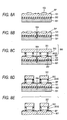
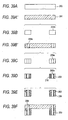
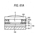
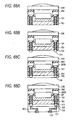
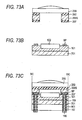
- the reference numeral 100 to an IT-CCD substrate 101 to a silicon substrate 102 to an IT-CCD; 200 to a sealing cover glass; 201 to a glass substrate; 203S to an spacer.
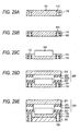
- a solid-state imaging device has such a structure that a glass substrate 201 to be a translucent member is bonded to the surface of an IT-CCD substrate 100 comprising a silicon substrate 101 to be a semiconductor substrate provided with an IT-CCD 102 through a spacer 203S in order to have a gap C corresponding to the light receiving region of the silicon substrate 101, and furthermore, the peripheral edge of the silicon substrate 101 is individually isolated by dicing, and an electrical connection to an external circuit (not shown) can be achieved through a bonding pad BP formed on the surface of the silicon substrate 101 in the peripheral edge portion exposed from the glass substrate 201.
- the spacer 203S has a height of 10 to 500 ⁇ m, and preferably 80 to 120 ⁇ m. Further, a spacer width is set to be approximately 100 to 500 ⁇ m.
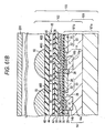
- the IT-CCD substrate has the IT-CCD arranged on the surface thereof, and furthermore, is constituted by the silicon substrate 101 provided with an RGB color filter 46 and a microlens 50.
- a channel stopper 28 is provided in a p well 101b formed on the surface of an n-type silicon substrate 101a, and a photodiode 14 and an electric charge transfer element 33 are formed with the channel stopper 28 interposed therebetween.
- an n-type impurity region 14b is provided in a p+ channel region 14a to form the photodiode 14.
- a vertical charge transfer channel 20 comprising an n-type impurity region having a depth of approximately 0.3 ⁇ m is formed in the p+ channel region 14a, and a vertical charge transfer electrode 32 comprising a polycrystalline silicon layer is formed on the vertical charge transfer channel 20 through a gate insulating film 30 comprising a silicon oxide film so that an electric charge transfer element 33 is constituted.
- a channel 26 for a reading gate is formed by the p-type impurity region between the electric charge transfer element 33 and the photodiode 14 on the side where a signal charge is read onto the vertical charge transfer channel 20.
- the n-type impurity region 14b is exposed from the surface of the silicon substrate 101 along the channel 26 for a reading gate and a signal charge generated in the photodiode 14 is temporarily stored in the n-type impurity region 14b and is then read through the channel 26 for a reading gate.
- the channel stopper 28 comprising a p+ type impurity region is present between the vertical charge transfer channel 20 and another photodiode 14. Consequently, the photodiode 14 and the vertical charge transfer channel 20 are electrically isolated from each other and the vertical charge transfer channels 20 are isolated so as not to come in contact with each other.
- the vertical charge transfer electrode 32 covers the channel 26 for a reading gate, and the n-type impurity region 14b is exposed and a part of the channel stopper 28 is exposed. A signal charge is transferred from the channel 26 for a reading gate which is provided below any vertical charge transfer electrode 32 to which a reading signal is applied.
- the vertical charge transfer electrode 32 constitutes, together with the vertical charge transfer channel 20, a vertical charge transfer device (VCCD) 33 for transferring a signal charge generated by the pn junction of the photodiode 14 in a vertical direction.
- the surface of the substrate provided with the vertical charge transfer electrode 32 is covered with a surface protective film 36 and a shielding film 38 formed of tungsten is provided thereon, and only a light receiving region 40 of the photodiode is opened and other regions are shielded.
- the upper layer of the vertical charge transfer electrode 32 is covered with a flattened insulating film 43 for surface flattening and a translucent resin film 44 formed on an upper layer thereof, and furthermore, a filter layer 46 is formed thereon.
- the filter layer 46 has a red filter layer 46R, a green filter layer 46G and a blue filter layer 46B arranged sequentially in order to make a predetermined pattern corresponding to each photodide 14.
- the upper layer is covered with a microlens array comprising a microlens 50 formed by patterning a translucent resin containing a photosensitive resin having a refractive index of 1.3 to 2.0 by an etching method using photolithography through a flattened insulating film 48 and then fusing the same translucent resin, and rounding the fused translucent resin by a surface tension and thereafter cooling the rounded translucent resin.
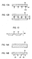
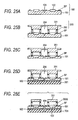
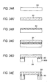
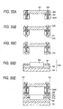
- This method is based on a so-called wafer level CSP method in which positioning is carried out on a wafer level, collective mounting and integration are performed and isolation for each IT-CCD is then executed as shown in views illustrating the manufacturing process in Figs. 2A to 2C and Fig. 3A to 3C .
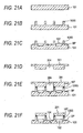
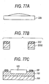
- This method is characterized in that a sealing cover glass 200 having a spacer which is provided with a spacer 203S in advance is used.
- a silicon substrate 203 to be a spacer is stuck to the surface of a glass substrate 201 through an adhesive layer 202 comprising an ultraviolet curing type adhesive (a Cation Polymerizing Energy Line Curing Adhesive).
- an ultraviolet curing type adhesive a Cation Polymerizing Energy Line Curing Adhesive
- CG1 Cation Polymerizing Energy Line Curing Adhesive
- a material having fewer portions to be an ⁇ ray radiation nucleus should be used for the glass substrate 201 to be utilized.
- an ⁇ ray limit value should be 0.002 (DPH/cm 2 ).
- the silicon substrate 203 is etched by an etching method using the photolithography with a resist pattern remaining in a portion to be the spacer, and the spacer 203S is thus formed.
- a resist is filled in a spacer region excluding an element region in a state in which the resist pattern for forming the spacer 203S is left, and the glass substrate is etched to have a predetermined depth. Consequently, an element trench section 204 is formed as shown in Fig. 2D .
- the spacer width should be set to be approximately 100 to 500 ⁇ m. If the spacer width is smaller than 100 ⁇ m, there is a possibility that sealing might be insufficient, and furthermore, a defective strength might be generated. If the spacer width is more than 500 ⁇ m, furthermore, there is a problem in that a division (the number of units which can be taken out of one wafer) is decreased and a size cannot be reduced. Moreover, it is desirable that a distance between the light receiving surface and the spacer should be set to be 50 ⁇ m or more in consideration of the exudation of an adhesive.
- The' spacer is formed by the silicon substrate. If the etching is carried out on such an etching condition that the etching speed of silicon oxide to be the main component of the glass substrate is much higher than the etching speed of silicon, therefore, it is also possible to perform the etching in a state in which the side walls of the spacer is maintained to be exposed in the element region. In the formation of the element trench section 204, it is also possible to use a dicing blade (grindstone).
- the etching condition may be selected in such a manner that a stuck foreign substance has a size of 5 ⁇ m or less in the etching of the spacer.
- a stuck foreign substance has a size of 5 ⁇ m or less, it is possible to prevent an image noise from being generated if a distance between the light receiving surface and the lower surface of the glass substrate is set to be 0.08 mm or morse as will be described below.
- an adhesive layer 207 is further formed on the surface of the spacer.
- the adhesive layer 207 should have a thickness of 5 ⁇ m or less. If the thickness is equal to or less than 5 ⁇ m, a bubble having a thickness of 5 ⁇ m or more is not present. If the distance between the light receiving surface and the lower surface of the glass substrate which will be described below is set to be 0.08 mm or more as described above, it is possible to prevent the image noise from being generated.
- the photolithography may be carried out again to form such a resist pattern as to include the whole side wall of the spacer, and the etching may be carried out through the resist pattern, thereby forming the trench section 204.
- the sealing cover glass 200 provided with the trench section 204 and the spacer 203S is obtained.
- the spacer should have a height of 0.088 mm or more in order to prevent the generation of the image noise and should be 0.12 mm or less in order to increase a productivity of the formation of the spacer.
- the spacer 203S is to be formed by the etching, it is also possible to carry out the etching while protecting the side walls of the spacer by using a C 4 F 8 plasma.
- a bottom surface should be etched by anisotropic etching using an SF 6 +O 2 plasma.
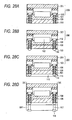
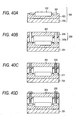
- an IT-CCD substrate is formed.
- the silicon substrate 101 (a 6-inch wafer is used) is prepared in advance and a cut trench 104 is formed by a method such as etching in a region corresponding to ah isolating line for isolation into each IT-CCD over the surface of the silicon substrate 101.
- a channel stopper layer is formed, a channel region is formed and an element region such as an electric charge transfer electrode ⁇ is formed.
- a bonding pad BP which is provided with a wiring layer on a surface and comprises a gold layer for an external connection.
- an alignment is carried out with an alignment mark formed in the peripheral edge portion of each substrate, and the sealing cover glass 200 is mounted on the IT-CCD substrate 100 provided with the element region as described above and is thus heated so that both of them are integrated With the adhesive layer 207.
- this process should be executed in a vacuum or an inert gas atmosphere such as a nitrogen gas.
- a thermosetting and ultraviolet curing adhesive as well as a thermosetting adhesive.
- the surface of the IT-CCD substrate is formed of Si or metal, moreover, it is also possible to carry out bonding through surface activating cold bonding without using an adhesive.
- CMP chemical mechanical polishing
- the CMP is carried out from the back side of the silicon substrate 101 in the same manner to execute polishing up to the cut trench 104 portion. Consequently, individual solid-state imaging devices can be obtained by the isolation.
- the trench section 204 is previously formed on the glass substrate 201 and the surface is removed to have such a depth as to reach the trench section 204 by a method such as the CMP after the mounting. Therefore, the isolation can be carried out very easily.
- a structure in which the edge of the glass substrate 201 is positioned on the inside of the edge of the silicon substrate 101 provided with the IT-CCD and the surface of the silicon substrate 101 is exposed can be formed with high precision in a very simple process in which a concave portion is previously formed on the inside of the' glass substrate and the removal is carried out to have the same depth by a method such as etch back or CMP after bonding.
- the structure can easily be formed with a high workability.
- the individual IT-CCDs can be formed by only isolation or polishing in a state in which an element formation surface is enclosed in a gap C by the bonding. Consequently, it is possible to provide an IT-CCD which rarely damages the element and has a high reliability.
- the silicon substrate is thinned to have a depth of approximately 1/2 by the CMP. Therefore, a size and a thickness can be reduced. Furthermore, the thickness is reduced after the bonding to the glass substrate. Consequently, it is possible to prevent a deterioration in a mechanical strength.
- the bonding pad BP provided on the silicon substrate constituting the IT-CCD substrate 100 is exposed from the sealing section formed by the spacer 203S and the glass substrate 201. Therefore, the formation can easily be carried out.
- the wiring layer including the bonding pad is constituted by a gold layer in the first embodiment, it is apparent that the gold layer is not restricted but another metal such as aluminum or another conductor layer such as silicide can be used.
- the microlens array can also be provided by forming a transparent resin film on the surface of a substrate and forming a lens layer having a refractive index gradient in a predetermined depth by ion implantation from the same surface.
- the spacer furthermore, it is possible to properly select a 42-alloy, metal, a glass, photosensitive polyimide and a polycarbonate resin in addition to the silicon substrate.
- the temperature for bonding is set to a room temperature or a temperature from 20 degree C to 80 degree C.
- the adhesive used for bonding it is preferable to use, for example, an epoxy adhesive, an oxetanyl adhesive, silicon adhesive, acrylic adhesive, UV curing adhesive, visible curing adhesive, or such, so that the adhesive line may be thin in order to obtain a predetermined adhesive force, prevent a permeation of water, and realize a high reliable bonding.
- frequency of distortion is measured when a temperature for bonding is changed.
- the temperature for bonding is changed to 20 degree C, 25 degree C, 50 degree C, 80 degree C, and 100 degree C.
- frequency of distortions is checked in each case of using a room temperature setting adhesive and a thermosetting adhesive.
- the adhesives mentioned above are applied for bonding of a glass substrate and a spacer and bonding of a spacer and an IT-CCD substrate.
- the temperature for bonding is preferably set under 80 degree C.
- the temperature for bonding is set equal to/ under 50 degree C. Therefore, the generation of distortion never occurred and it is possible to obtain an excellent result.
- Simulation conditions were set to have an exit pupil of 3.5 mm, an F value of 3.5 and a refractive index of a glass substrate of 1.5.
- the distance between the light receiving surface and the glass substrate is 0.07 mm, the density of the shadow is 4.7% which is more than 4%. Accordingly, it is desirable that the distance between the light receiving surface and the glass substrate should be equal to or more than 0.08 mm.
- Table 2 shows a result obtained by measuring the relationship between a distance between the light receiving surface and the upper surface of the glass substrate and the density of a shadow in which a defect is projected onto a solid-state imaging element in the case in which a defect having a size of 20 ⁇ m is present on the upper surface of the glass substrate.
- Table 2 Distance (mm) between Light-receiving surface and upper surface Density of shadow (%) 0.3 8.3 0.4 5.1 0.5 3.5 0.6 2.5 0.7 1.9 0.8 1.5 0.9 1.2 1.0 1.0
- the density of the shadow is equal to or more than 4%.
- the density of the shadow projected onto the light receiving surface of the solid-state imaging element is 4% and the shadow is started to be seen over a printed image.
- the density of the shadow is set to be less than 4%, therefore, there is no influence of such a defect.
- an interval between the surface of the glass substrate and the CCD is to be 0.08 mm. It is apparent that the interval should be desirably set to be 0.12 mm.
- the distance between the light receiving surface and the upper surface of the glass substrate is equal to or more than 0.5 mm even if a dust having a size of 20 ⁇ m is put on the surface of the glass substrate.
- the distance from the light receiving surface and the upper surface of the glass substrate is equal to or more than 1.5 mm with an F value of 11.
- the distance between the light receiving surface and the upper surface of the glass substrate is set to be 0.5 to 1.5 mm, an invisible dust can be prevented from making an image noise if any.
- the distance between the light receiving surface and the surface of the glass substrate should be set to be 1.5 mm or less in consideration of the problem of the size of the device, a strength and a deterioration in the productivity of dicing because of a great glass thickness.
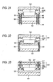
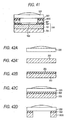
- the cut trench 104 is previously formed on the silicon substrate 101 constituting the IT-CCD substrate 100, the IT-CCD substrate 100 and the sealing cover glass 200 are bonded to each other by using the spacer 203S formed of the same silicon as that of the solid state image pick-up element substrate 100, and the CMP is then carried out to reach the cut trench 104 from the back side so that the thickness of the silicon substrate 101 is reduced and the isolation is executed simultaneously.
- This example is characterized in that the isolation is carried out without forming the cut trench on the silicon substrate 101 and an exact thickness is maintained. Other portions are formed in the same manner as those in the first embodiment.
- Figs. 4A to 4D show bonding and isolating steps.
- the silicon substrate 101 is set to be a starting material, and a channel stopper layer is formed, a channel region is formed and an element region such as an electric charge transfer electrode or such is formed by using an ordinary silicon process.
- a bonding pad BP which is provided with a wiring layer on a surface and comprises a gold layer for an external connection.
- a sealing cover glass 200 is mounted on an IT-CCD substrate 100 formed as described above and is thus heated so that both of them are integrated with an adhesive layer 207.
- a cut trench is not formed on the silicon substrate 101, a mechanical strength is great.
- CMP chemical mechanical polishing
- cutting is carried out by means of a diamond blade (a grindstone) from the glass substrate 201 side so that isolation into individual solid-state imaging devices is performed.
- a diamond blade a grindstone
- the cut trench 104 is previously formed on the silicon substrate 101 constituting the IT-CCD substrate 100 and the CMP is then carried out to reach the cut trench 104 from the back side after the bonding so that the thickness of the silicon substrate 101 is reduced and the isolation is executed simultaneously.
- a dummy plate 301 formed by a silicon substrate having a thickness of 50 to 700 ⁇ m is stuck to the back side of the silicon substrate 101 through an adhesive layer 302 and a cut trench 304 having such a depth as to reach the dummy plate 301 is formed after the sticking.
- the adhesive layer 302 may be softened to eliminate an adhesiveness, thereby removing the dummy plate 301.
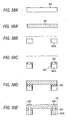
- Figs. 5A to 5E show the bonding and isolating steps.
- the silicon substrate 101 is set to be a starting material, and a channel stopper layer is formed, a channel region is formed and an element region such as an electric charge transfer electrode ... is formed by using an ordinary silicon process.
- a bonding pad BP which is provided with a wiring layer on a surface and comprises a gold layer for an external connection.
- the dummy plate 301 formed by a silicon substrate is stuck to the back side of the silicon substrate 101 through the adhesive layer 302.
- the cut trench 304 is formed by using a diamond blade (a grindstone) from the element formation surface side of the silicon substrate 101.
- an alignment is carried out with an alignment mark (not shown) formed on the peripheral edge portions of an IT-CCD substrate 100 and a sealing cover glass 200, and the sealing cover glass 200 is mounted on the IT-CCD substrate 100 formed as described above and is thus heated so that both of them are integrated with an adhesive layer 207.
- the glass substrate comprising a spacer 203S and the adhesive layer 207 formed at the steps in Figs. 2A to 2C is used.
- the cut trench 304 is formed to penetrate through the silicon substrate 101, a mechanical strength is great because of the fixation of the dummy plate 301.
- CMP chemical mechanical polishing
- the adhesive layer 302 provided on the back face of the silicon substrate 101 is softened to remove the dummy plate 301, thereby carrying out isolation into individual solid-state imaging devices. It is desirable that a material having a lower softening point than that of the adhesive layer 202 for bonding the spacer 203S to the glass substrate 201 should be selected for the adhesive layer 302.
- the IT-CCD substrate 100 is subjected to dicing over the dummy plate 301 prior to the bonding.
- a stress to be applied after the bonding is lessened and a manufacturing yield can be more enhanced.
- the bonding of the glass substrate to the space may be carried out by using the adhesive layer in the embodiments, it is also possible to apply anode bonding or surface activating cold bonding. According to the anode bonding, it is possible to easily obtain firm bonding.
- the CMP has been used in the reduction in the thickness of the glass substrate in the first to third embodiments, it is also possible to apply a grinding method, a polishing method and an etching method.
- the trench section 204 is previously formed in the region corresponding to the element region of the glass substrate 201 constituting the sealing cover glass 200, the IT-CCD substrate is bonded to the glass substrate and the CMP is then carried out from the back side of the glass substrate 201, thereby performing isolation into the individual elements.
- a glass substrate having no concave portion is bonded and the periphery of a cutting line is evaporated by dicing or laser during isolation, and the edge of the glass substrate 201 of each IT-CCD is regulated to be placed on the inside of the edge of the silicon substrate 101 constituting the IT-CCD substrate 100.
- Other portions are formed in the same manner as those in the first embodiment.
- the processing of the glass substrate is completed when the spacer is formed as shown in Fig. 2B .
- a glass substrate obtained by bonding a spacer 203S to the plate-shaped glass substrate 201 is used as a starting material.
- the silicon substrate 101 (a 6-inch wafer is used) is prepared in advance and a cut trench 104 is formed by a method such as etching in a region corresponding to an isolating line for isolation into each IT-CCD.
- a channel stopper layer is formed, a channel region is formed and an element region such as an electric charge transfer electrode ⁇ is formed.
- a bonding pad BP which is provided with a wiring layer on a surface and comprises a gold layer for an external connection.
- a sealing cover glass 200 is mounted on the IT-CCD substrate 100 formed as described above and is thus heated so that both of them are integrated with an adhesive layer 207.
- the periphery of a cutting line is evaporated from the back side of the glass substrate by dicing or laser and the edge of the glass substrate 201 of each IT-CCD is regulated to be placed on the inside of the edge of the silicon substrate 101 constituting the IT-CCD substrate 100.
- the CMP is carried out from the back side of the silicon substrate 101 in the same manner to carry out polishing up to the cut trench 104 portion, thereby performing isolation into individual solid-state imaging devices. Moreover, this step is not restricted to the CMP but grinding, polishing and etching may be used.
- the trench section 204 is not previously formed on the glass substrate 201 but the edge is removed by the evaporation through the dicing or the laser. Consequently, the isolation can be carried out very easily.
- the structure in which the edge of the glass substrate 201 is placed on the inside of the edge of the silicon substrate 101 mounting a CCD and the surface of the silicon substrate 101 is exposed can be formed with high precision by a simple process for carrying out the evaporation through the dicing or the laser.
- the glass substrate maintains the same thickness till the isolating step. Consequently, it is possible to reduce a warp and a strain.
- the cut trench 104 is previously formed on the silicon substrate 101 constituting the IT-CCD substrate 100 and the CMP is then carried out to reach the cut trench 104 from the back side after the bonding so that the thickness of the silicon substrate 101 is reduced and the isolation is executed simultaneously.
- This example is characterized in that a cut trench is not formed on the silicon substrate 101 but isolation is carried out and an exact thickness is maintained.
- bonding is carried out without the formation of a trench section 204 on a glass substrate 201 and an edge portion is evaporated during the isolation. Other portions are formed in the same manner as those in the first embodiment.
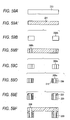
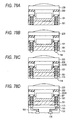
- Figs. 7A to 7D show the bonding and isolating steps.
- the silicon substrate 101 is set to be a starting material, and a channel stopper layer is formed, a channel region is formed and an element region such as an electric charge transfer electrode, or such is formed by using an ordinary silicon process.
- a bonding pad BP which is provided with a wiring layer on a surface and comprises a gold layer for an external connection.
- the periphery of the cutting line is evaporated from the back side of the glass substrate 201 by dicing or laser and the edge of the glass substrate 201 of each IT-CCD is regulated to be placed on the inside of the edge of the silicon substrate 101 constituting the IT-CCD substrate 100 and isolation is thus performed in the same manner as in the fourth embodiment.
- cutting is carried out by means of a diamond blade (a grindstone) from the glass substrate 201 side so that the isolation into individual solid-state imaging devices is performed.
- the method it is possible to form a device which is thicker than the solid-state imaging device obtained in the first embodiment and has a high reliability.
- the cut trench 104 is previously formed on the silicon substrate 101 constituting the IT-CCD substrate 100 and the CMP is then carried out from the back side so that the isolation is executed.
- the cut trench 104 is previously formed on the silicon substrate 101 constituting the IT-CCD substrate 100 and cutting is carried out by means of a diamond blade (a grindstone) after bonding, thereby isolating the silicon substrate 101.
- a dummy plate 301 formed by a silicon substrate having a thickness of 50 to 700 ⁇ m is stuck to the back side of the silicon substrate 101 through an adhesive layer 302 and a cut trench 304 having such a depth as to reach the dummy plate 301 is formed after the sticking in such a manner that the isolation of the silicon substrate 101 is not required after the sticking of a sealing cover glass 200 to the IT-CCD substrate 100.
- the adhesive layer 302 can be softened to remove the dummy plate 301.
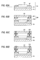
- Figs. 8A to 8E show the bonding and isolating steps.
- the silicon substrate 101 is set to be a starting material, and a channel stopper layer is formed, a channel region is formed and an element region such as an electric charge transfer electrode, or such is formed by using an ordinary silicon process.
- a bonding pad BP which is provided with a wiring layer on a surface and comprises a gold layer for an external connection.
- the dummy plate 301 formed by a silicon plate having a thickness of 50 to 700 ⁇ m is stuck to the back side of the silicon substrate 101 through the adhesive layer 302.
- the cut trench 304 is formed by using a diamond blade (a grindstone) from the element formation surface side of the silicon substrate 101.
- an alignment is carried out with an alignment mark (not shown) formed in the peripheral edge portions of the IT-CCD substrate 100 and the sealing cover glass 200, and the sealing cover glass 200 is mounted on the IT-CCD substrate 100 formed as described above and is thus heated so that both of them are integrated with an adhesive layer 207.
- the glass substrate comprising the spacer 203S and the adhesive layer 207 formed at the steps in Figs. 8A to 8C is used. In this case, although the cut trench 304 is formed to penetrate through the silicon substrate 101, a mechanical strength is great because of the fixation of the dummy plate 301.
- the periphery of a cutting line is evaporated from the back side of a glass substrate 201 by dicing or laser and the edge of the glass substrate 201 of each IT-CCD is regulated to be placed on the inside of the edge of the silicon substrate 101 constituting the IT-CCD substrate 100, and isolation is thus performed in the same manner as in the fourth embodiment.
- the adhesive layer 302 provided on the back face of the silicon substrate 101 is softened to remove the dummy plate 301, thereby performing the isolation into the individual solid-state imaging devices. It is desirable that a material having a lower softening point than that of the adhesive layer 202 for bonding the spacer 203S to the glass substrate 201 should be selected for the adhesive layer 302.
- the IT-CCD substrate 100 is subjected to dicing over the dummy plate 301 prior to the bonding.
- a stress to be applied after the bonding is lessened and a manufacturing yield can be more enhanced.
- the glass substrate may be cut by scribing or etching.
- the dummy plate 301 formed by a silicon plate having a thickness of 50 to 700 ⁇ m is stuck to the back side of the silicon substrate 101 through the adhesive layer 302 and the cut trench 304 having such a depth as to reach the dummy plate 301 is formed after the sticking, and the adhesive layer 302 is softened to remove the dummy plate 301, thereby carrying out the isolation at the step of performing the isolation into the individual IT-CCDs after the bonding to the glass substrate 201.
- a dummy plate 401 formed by a glass plate having a thickness of 50 to 700 ⁇ m is stuck to the back side of a glass substrate 201 through an adhesive layer 402 and a concave portion 404 having such a depth as to reach the dummy plate 401 is formed after the sticking.
- the adhesive layer 402 is softened to remove the dummy plate 401, thereby carrying out the isolation.
- Other portions are formed in the same manner as those in the sixth embodiment.
- a silicon substrate on which neither a cut trench nor a dummy plate is previously formed is used and is finally cut and isolated by means of a diamond blade (a grindstone).
- the dummy plate 401 formed by a glass plate having a thickness of 50 to 700 ⁇ m is stuck to the back side of the glass substrate 201 through the adhesive layer 402, and furthermore, a silicon substrate 203 is stuck through an adhesive layer 202 after the sticking and the silicon substrate 203 is formed into a spacer 203S by an etching method using photolithography in the same manner as in the first embodiment illustrated in Figs. 2A to 2C .
- a region corresponding to an IT-CCD is selectively etched again and a concave portion 404 having such a depth as to reach the dummy plate 401 is formed in the same manner as in the first embodiment. Moreover, the formation may be carried out by half dicing.
- the silicon substrate 101 is set to be a starting material, and a channel stopper layer is formed, a channel region is formed and an element region such as an electric charge transfer electrode ⁇ is formed by using an ordinary silicon process.
- a bonding pad BP which is provided with a wiring layer on a surface and comprises a gold layer for an external connection.
- an alignment is carried out with an alignment mark (not shown) formed in the peripheral edge portions of the IT-CCD substrate 100 thus formed and a sealing cover glass 200, and the sealing cover glass 200 having the dummy plate 401 is mounted on the IT-CCD substrate 100 formed as described above and is thus heated so that both of them are integrated with an adhesive layer 207.
- the IT-CCD substrate formed by the silicon substrate 101 is cut by using a diamond blade (a grindstone) to carry out isolation into individual solid-state imaging devices.
- the glass substrate 201 constituting the sealing cover glass 200 is isolated by dicing or etching in advance over the dummy plate 401 prior to the bonding.
- a stress to be applied after the bonding is lessened and a manufacturing yield can be more enhanced.
- the bonding is exactly carried out without previously forming the cut trench 104 on the silicon substrate 101 constituting the IT-CCD substrate 100 and the cutting is finally performed by using the diamond blade (the grindstone).
- This example is characterized in that the cut trench 104 is previously formed on the silicon substrate 101 constituting the IT-CCD substrate 100 and CMP is carried out to reach the cut trench 104 from the back side after bonding, thereby performing isolation while reducing the thickness of the silicon substrate 101.
- Other portions are formed in the same manner as those in the seventh embodiment.
- Figs. 10A to 10D show the bonding and isolating steps.
- the silicon substrate 101 provided with the cut trench 104 is set to be a starting material, and a channel stopper layer is formed, a channel region is formed and an element region such as an electric charge transfer electrode ⁇ is formed by using an ordinary silicon process.
- a bonding pad BP which is provided with a wiring layer on a surface and comprises a gold layer for an external connection.
- an alignment is carried out with an alignment mark formed in the peripheral edge portion of each substrate, and the sealing cover glass 200 having the dummy substrate 401 formed as in the seventh embodiment is mounted on the IT-CCD substrate 100 and both of them are integrated by cold direct bonding. While the formation is carried out by the direct bonding without using an adhesive layer, the bonding may be performed with an adhesive layer 207.
- CMP chemical mechanical polishing
- heating is carried out to soften an adhesive layer 402, thereby removing the dummy substrate 401.
- the isolation can easily be carried out so that the solid-state imaging device is formed.
- the bonding is exactly carried out without previously forming the cut trench 104 on the silicon substrate 101 constituting the IT-CCD substrate 100 and the cutting is finally performed by using the diamond blade (the grindstone).
- a dummy plate is previously formed on the silicon substrate 101 constituting the IT-CCD substate 100 and a glass substrate 201 constituting a sealing cover glass 200, and the cut trench 104 and a trench section 204 are previously formed prior to bonding, and adhesive layers 402 and 302 are softened to remove dummy plates 301 and 401, thereby carrying out isolation after the bonding.
- Other portions are formed in the same manner as those in the seventh embodiment.
- Figs. 11A to 11D show the bonding and isolating steps.
- the silicon substrate 101 having the dummy plate 301 stuck thereto is set to be a starting material, and a channel stopper layer is formed, a channel region is formed and an element region such as an electric charge transfer electrode ⁇ is formed by using an ordinary silicon process.
- a bonding pad BP which is provided with a wiring layer on a surface and comprises a gold layer for an external connection.
- a cut trench 304 is formed to reach the dummy plate 301.
- the dummy plate 401 is stuck to the sealing cover glass 200 in the same manner as in the seventh and eighth embodiments, and furthermore, a concave portion 404 is formed by etching or dicing.
- the adhesive layers 402 and 203 are softened to remove the dummy plates 301 and 401 so that isolation into individual IT-CCDs can be carried out.
- These adhesive layers 302 and 402 to be used may have almost equal softening temperatures and may be thus softened at the same time.
- one of the adhesive layers 302 and 402 may be removed to carry out fixation by taping, and the other adhesive layer 302 or 402 may be softened to be removed.
- the silicon substrate 203 to be a spacer is stuck to the glass substrate 201 through an adhesive, and the silicon substrate 203 is subjected to the patterning to form the cut trench 204 by an etching method using photolithography in the formation of the sealing cover glass 200 provided with the spacer 203S as shown in Figs. 2A and 2B .
- the spacer 203S is etched over a dummy plate by using a dummy plate 501 and sticking to the glass substrate 201 is then carried out with an adhesive layer 202.
- Other portions are formed in the same manner as those in the embodiments.
- the silicon substrate 203 to be the spacer is stuck to the dummy plate 501 formed by a silicon substrate through an adhesive layer 502 having a softening temperature of approximately 50 to 150degree C. Then, the silicon substrate 203 is subjected to patterning by an etching method using photolithography, thereby forming the spacer 203S.
- the glass substrate 201 is stuck to the spacer 203S side through the adhesive layer 202 having a softening temperature of approximately 100 to 200 degree C.
- the glass substrate 201 is stuck and heating is then carried out up to approximately 50 to 150 degree C to soften the adhesive layer 502, thereby removing the dummy plate 501. Consequently, the sealing cover glass 200 having a spacer is formed.
- the adhesive layer 502 for sticking the dummy plate is resistant to a baking temperature in a photolithographic process. Moreover, since the dummy plate 501 needs to be removed, the adhesive layer 202 for sticking the spacer 203S to the glass substrate 201 needs to have a much higher softening temperature than that of the adhesive layer 502.
- the trench section 204 should be formed by dicing or etching prior to the sticking as shown in Fig. 13 . Furthermore, it is preferable that a concavo-convex portion should be formed by the dicing or the etching after the dummy plate 501 is removed.
- the bonding step and the cutting step are the same as those in Figs. 3 to 5 described in the first to third embodiments.
- a concave portion 205 is formed and a spacer 206 is thus provided on a glass substrate 201 by an etching method using photolithography in this example.
- Other portions are formed in the same manner as those in the embodiments.
- the glass substrate 201 is prepared.
- the concave portion 205 is formed by the etching method using the photolithography. Consequently, a glass substrate comprising the spacer 206 is formed.
- the spacer 206 is integrally formed. Therefore, manufacture can easily be carried out and a shift is not generated, and furthermore, there is no possibility that a strain might be generated in a bonded portion.
- a concave portion 205 is formed on a glass substrate 201 by an etching method using photolithography so that the spacer 206 is formed integrally. Then, the trench section 204 is formed. Consequently, the trench section 204 of the glass substrate for positioning the edge of the sealing cover glass 200 on the inside of the edge of an IT-CCD substrate 100 is formed by the etching. Accordingly, the generation of a strain is reduced and the isolating step can be thereby carried out easily.
- the glass substrate 201 is prepared.
- the concave portion 205 is formed on the glass substrate 201 by the etching method using the photolithography.
- the etching is further carried out more deeply by the etching method using the photolithography to form the trench section 204.
- the spacer 206 is formed integrally.
- a resist pattern is also possible to form a resist pattern to be a mask in a two-layer structure, to etch the trench section 204 for forming the spacer, and to then remove only the resist pattern of an upper layer selectively, thereby carrying out the etching using, as a mask, only the resist pattern on the lower layer side.
- the trench section 204 is formed on the glass substrate 201 by the etching method using the photolithography and the spacer 206 is formed integrally, and furthermore, the trench section 204 of the glass substrate 201 for positioning the edge of the sealing cover glass 200 on the inside of the edge of an IT-CCD substrate 100 is formed by the etching. Accordingly, the generation of a strain can be reduced and the isolating step can easily be carried out.
- the glass substrate 201 is prepared.
- the trench section 204 is formed on the glass substrate 201 by the etching method using the photolithography.
- the silicon substrate 203 to be a substrate for a spacer is stuck through an adhesive layer 202.
- the spacer 203S is formed integrally by the etching method using the photolithography.
- the silicon substrate 203 to be a spacer is stuck to the glass substrate 201 through an adhesive, and the silicon substrate 203 is subjected to the patterning to form the sealing cover glass 200 by an etching method using photolithography so that the sealing cover glass 200 is formed as shown in Figs. 16A to 16D .
- a spacer 203S is subjected to the patterning over a dummy plate by using a dummy plate 501 and sticking to the glass substrate 201 provided with a trench section 204 is then carried out with an adhesive layer 202.
- Other portions are formed in the same manner as those in the thirteenth embodiment.
- the silicon substrate 203 to be the spacer is stuck to the dummy plate 501 formed by a silicon substrate through an adhesive layer 502 having a softening temperature of approximately 50 to 150 degree C. As shown in Fig. 17A , then, the silicon substrate 203 is subjected to the patterning by the etching method using the photolithography, thereby forming the spacer 203S.
- the glass substrate 201 having the trench section 204 is stuck to the spacer 203S side through the adhesive layer 202 having a softening temperature of approximately 100 to 200 degree C.
- the glass substrate 201 is stuck and heating is then carried out up to approximately 50 to 150 degree C to soften the adhesive layer 502, thereby removing the dummy plate 501. Consequently, the sealing cover glass 200 having a spacer is formed as shown in Fig. 17C .
- the fifteenth to seventeenth embodiments are characterized in that sticking to a dummy plate 401 is carried out and the trench section 204 is formed so that the glass substrate itself is previously isolated prior to the bonding, and an adhesive layer 402 is softened after the bonding, thereby removing the dummy plate and carrying out isolation into individual IT-CCDs.
- Other portions are formed in the same manner as those in the fourteenth embodiment.
- the trench section 204 is formed on the glass substrate of a sealing cover glass of a spacer member type and the glass substrate can easily be isolated in the embodiments shown in Figs. 15A to 15C , the dummy plate 401 formed by the glass substrate is used through the adhesive layer 402, and the dummy plate is removed so that the isolation can easily be carried out as shown in Fig. 18 .
- a glass plate is used as a starting material, and the trench section 204 and a spacer 26 are formed by an etching method using photolithography after the dummy plate is stuck.
- the adhesive layer 402 is only softened by heating during division and the division can be thereby carried out very easily.
- the bonding and isolating steps are the same as those described in the seventh to ninth embodiments.
- This example is characterized in that the glass substrate 201 of such a type as to stick the spacer 203S to the glass plate having a concave portion described in the thirteenth embodiment is stuck to a dummy plate 401 and a trench section 204 is formed so that the glass substrate itself is previously isolated prior to the bonding, and an adhesive layer 402 is softened after the bonding, thereby removing the dummy plate and carrying out isolation into individual IT-CCDs. Other portions are formed in the same manner as those in the thirteenth embodiment.
- the dummy plate 401 is stuck through the adhesive layer 402 to the spacer member type glass plate according to the embodiment shown in Figs. 16A and 16B and the trench section 204 is formed as shown in Figs. 19A and 19B .
- a glass plate is used as a starting material, and the trench section 204 having such a depth as to reach the dummy plate and the spacer 203S are formed in the same manner as in the thirteenth embodiment after the dummy plate is stuck.
- the dummy substrate 401 is stuck to the glass substrate 201 through the adhesive layer 402.
- the glass substrate 201 is etched by using photolithography and the trench section reaching the dummy substrate 401 from the surface of the glass substrate 201 is formed.
- a silicon substrate 203 for the spacer is stuck through an adhesive layer 202.
- the silicon substrate 203 is selectively removed by the etching method using the photolithography to form the spacer 203S.
- the bonding and isolating steps are the same as those described in the seventh to ninth embodiments.
- This example is characterized in that the glass substrate 201 of such a type as to stick the spacer 203S patterned over the dummy plate 501 to the glass plate having a concave portion described in the fourteenth embodiment ( Fig. 17 ) is stuck to a dummy plate 401 and a trench section 204 is formed so that the glass substrate itself.is previously isolated prior to the bonding, and an adhesive layer 402 is softened after the bonding, thereby removing the dummy plate and carrying out isolation into individual IT-CCDs. Other portions are formed in the same manner as those in the fourteenth embodiment.
- the dummy plate 401 is stuck to a spacer sticking type glass plate according to the embodiment shown in Figs. 17A and 17B through the adhesive layer 402 as shown in Figs. 20A to 20C .
- a glass plate is used as a starting material, and the trench section 204 having such a depth as to reach the dummy plate and the spacer 203S are formed in the same manner as in the fifteenth embodiment after the dummy plate is stuck.
- the silicon substrate 203 to be the spacer is stuck to a dummy plate 501 formed by a silicon substrate through an adhesive layer 502, and then, the silicon substrate 203 is subjected to patterning by an etching method using photolithography, thereby forming the spacer 203S as shown in Fig. 20A .
- the glass substrate 201 having the trench section 204 formed to reach the dummy plate 401 is stuck to the spacer 203S side through an adhesive layer 202.
- the glass substrate 201 is stuck and the adhesive layer 502 is then softened to remove the dummy plate 501 so that a sealing cover glass 200 having a spacer is formed as shown in Fig. 20C .
- the adhesive layer 402 is only softened by heating during division so that the dummy plate 401 can be removed readily and the division can be carried out very easily.
- the bonding and isolating steps are the same as those described in the seventh to ninth embodiments.
- a spacer 106S is formed integrally with a silicon substrate 101 constituting the IT-CCD substrate. Other portions are formed in the same manner as those in the embodiments.
- a resist pattern is formed on the surface of the silicon substrate 101 by photolithography as shown in Fig. 21A and a concave portion 105 is formed using the resist pattern as a mask by selective etching so that the spacer 106S is formed as shown in Fig. 21B .
- a channel stopper layer is formed, a channel region is formed and an element region such as an electric charge transfer electrode ⁇ is formed in an element formation region surrounded by the spacer 106S by using an ordinary silicon process.
- a bonding pad BP which is provided with a wiring layer on a surface and comprises a gold layer for an external connection.
- a glass substrate 201 provided with a trench section 204 is prepared as shown in Fig. 21D and an alignment is carried out opposite to the element formation surface of the IT-CCD substrate 100 and the glass substrate 201 is integrated as shown in Fig. 21E .
- the integration is firmly carried out by heating an adhesive layer 107 applied to the surface of the spacer 106S.
- the glass substrate side and the IT-CCD substrate side are thinned by CMP so that isolation into the IT-CCDs can be carried out.
- the thinning step is not restricted to the CMP but can be executed by grinding, polishing or etching.
- the trench section 204 is not formed on the glass substrate, moreover, cutting is carried out through dicing or laser so that the isolation can be performed with a high workability.
- the cutting is carried out by using a diamond blade so that the isolation can be performed with a high workability.
- the spacer is formed integrally with the IT-CCD substrate. Therefore, it is possible to form a solid-state imaging device having a high reliability without generating a strain in a bonded portion.
- a silicon substrate 108 may be stuck onto the IT-CCD substrate through an adhesive layer 107 so as to be subjected to patterning on the IT-CCD substrate in this example.
- Other portions are formed in the same manner as those in the eighteenth embodiment.
- a channel stopper layer is formed, a channel region is formed and an element region such as an electric charge transfer electrode ⁇ is formed on a silicon substrate 101 by using an ordinary silicon process as shown in Figs. 22A to 22C in this example.
- a bonding pad BP which is provided with a wiring layer on a surface and comprises a gold layer for an external connection.
- a silicon substrate 103 is stuck onto the IT-CCD substrate through the adhesive layer 107.
- the silicon substrate 103 is selectively removed from the IT-CCD substrate by an etching method using photolithography to form a spacer 103S.
- an adhesive layer 109 is applied onto the spacer 103S and a cut trench 104 is formed.
- the spacer is provided after the formation of the element region on the silicon substrate. Therefore, the spacer is not an obstacle in the formation of the element region and manufacture can easily be carried out. Since integral formation is not performed, there is also a problem in that a slight strain cannot be avoided.
- a dummy substrate 601 may be used to form the spacer 103S thereon and may be stuck to a silicon substrate 101 provided with an IT-CCD, that is, a substrate for the formation of the IT-CCD.
- IT-CCD that is, a substrate for the formation of the IT-CCD.
- Other portions are formed in the same manner as those in the nineteenth embodiment.
- a silicon substrate 103 to be the spacer is stuck to the dummy plate 601 formed by a silicon substrate through an adhesive layer 602 having a softening temperature of approximately 50 to 150 degree C. Then, the silicon substrate 103 is selectively removed by an etching method using photolithography, thereby forming the spacer 103S.
- the silicon substrate 101 provided with the IT-CCD is stuck to the spacer 103S side through an adhesive layer 202 having a softening temperature of approximately 100 to 200 degree C.
- the silicon substrate 201 provided with the IT-CCD is stuck and heating is then carried out to approximately 50 to 150 degree C to soften the adhesive layer 602, thereby removing the dummy plate 601 as shown in Fig. 23C .
- a cut trench 104 is formed so that an IT-CCD substrate 100 having a spacer is formed in the same manner as in Fig. 22B .
- the bonding and isolating steps for the glass substrate and the IT-CCD substrate are the same as those described in the eighteenth embodiment.
- cut trench 104 is provided after the formation of the spacer in the embodiment, it is apparent that the cut trench 104 may be provided before the formation of the spacer.
- the bonding of the glass substrate and the space and the bonding of the silicon substrate constituting the IT-CCD and the spacer are carried out by using the adhesive layer. It is possible to obtain firm bonding by carrying out surface activation and performing the bonding through cold direct bonding.
- the silicon substrate is used for the spacer in the first to twentieth embodiments (excluding the eleventh, twelfth and fifteenth embodiments), it is not restricted but a 42-alloy having a coefficient of thermal expansion which is almost equal to that of the IT-CCD substrate can also be applied. Furthermore, it is also possible to use a material having a coefficient of thermal expansion which is almost equal to that of a translucent substrate. In addition, a polyimide resin may be used. In this case, a flexibility can be obtained and an effect of absorbing a strain can also be produced for the generation of the strain due to a change in a temperature.
- the spacer may be formed by using an adhesive tape. In this case, it is possible to carry out a processing with high precision by cutting using a laser processing after sticking to a whole surface.
- the silicon substrate or the glass substrate is used for the dummy plate in the first to twentieth embodiments, it is not restricted but a metal plate can also be used. Furthermore, a flexible film may be used.
- thermosetting resin for the adhesive layer.
- cut trench is provided prior to the formation of the spacer in the eighteenth to twentieth embodiments, it is apparent that the cut trench may be provided after the formation of the spacer.
- the solid-state imaging device is characterized in that a reinforcing plate 701 formed by a silicon substrate bonded through a silicon oxide film (not shown) is stuck to the back side of a silicon substrate 101 constituting an IT-CCD substrate 100 of the solid-state imaging device according to the first embodiment.
- the reinforcing plate 701 formed by the silicon substrate having the silicon oxide film formed on a surface is bonded onto the IT-CCD substrate by direct bonding using surface activating cold bonding.
- the structure of the element is the same as that of the solid-state imaging device described in the first embodiment, and the silicon substrate is thinned to have an almost half thickness from the back face by a CMP method and the reinforcing plate 701 is bonded to the back face as shown in Fig. 24 in order to compensate for a reduction in a strength which is caused by the thinning.
- the IT-CCD substrate 100 can be thinned to increase a driving speed and a reduction in a strength which is caused by the thinning can be compensated by the reinforcing plate. Moreover, a moisture resistance can also be enhanced.
- a processing to be carried out till the step of sticking a glass substrate to the IT-CCD substrate is basically the same as that of the first embodiment. More specifically, as shown in Fig. 25A , an element region constituting the IT-CCD is formed by using an ordinary silicon process on the silicon substrate 101 provided with a cut trench 104 in advance, and furthermore, there is formed a bonding pad BP which is provided with a wiring layer on a surface and comprises a gold layer for an external connection.
- an alignment is carried out with an alignment mark formed in the peripheral edge portion of each substrate, and a sealing cover glass 200 is mounted on the IT-CCD substrate 100 provided with an element region as described above and heating is carried out to integrate both of them with an adhesive layer 202.
- This process may employ surface activating cold bonding.
- the glass substrate is maintained as it is and the CMP method is carried out from the back side of the silicon substrate 101 in the same manner to polish the cut trench 104 portion.
- the CMP method is carried out from the back side of the silicon substrate 101 in the same manner to polish the cut trench 104 portion.
- the reinforcing plate 701 formed by a silicon substrate having a silicon oxide film (not shown) provided on a surface is bonded to the back side of the thinned silicon substrate 101 by direct bonding using the surface activating cold bonding
- the reinforcing plate 701 is subjected to dicing by using a diamond blade (a grindstone), thereby forming a solid-state imaging device having a reinforcing plate as shown in Fig. 25E .
- the solid-state imaging device can be formed very easily.
- spacer is formed on the glass substrate in the embodiment, it is also possible to apply a spacer which is provided on the IT-CCD substrate or is provided separately.
- the reinforcing plate is constituted by the silicon substrate isolated from the IT-CCD substrate and is caused to have an adiabatic property in the embodiment, moreover, it is also possible to utilize a substrate having an excellent heat conductiveness for a radiation plate. According to the embodiment, furthermore, a moisture resistance can also be enhanced. In addition, also in the case in which the cut trench 104 is not provided, the embodiment can be applied.
- a shield plate 801 by sticking a metal substrate such as tungsten or chromium in place of the reinforcing plate as shown in Fig. 26 .
- Other portions are constituted in just the same manner.
- an electromagnetic wave can be shielded so that an unnecessary radiation noise can be reduced.
- the bonding pad formed on the surface of the IT-CCD substrate is formed to be exposed and the edge of the translucent substrate (glass substrate) 201 is formed to be placed on the inside of the edge of the IT-CCD substrate in such a manner that an electrical connection can be carried out over the surface of the IT-CCD substrate.
- This example is characterized in that the edges of an IT-CCD substrate and a glass substrate are constituted equally and the back side is fetched via a through hole H penetrating through an IT-CCD substrate 100 and a reinforcing plate 701 stuck to a back face thereof as shown in Fig. 27C .
- 108 denotes a conductor layer and 109 denotes a silicon oxide layer to be an insulating layer.
- a glass substrate 201 to be a translucent member is bonded to the surface of the IT-CCD substrate 100 comprising a silicon substrate 101 to be a semiconductor substrate provided with an IT-CCD 102 through a spacer S203 in order to have a gap C corresponding to the light receiving region of the silicon substrate 101, and furthermore, a pad 113 and a bump 114 are formed to be external fetch terminals which are formed on the back side of the IT-CCD substrate 100 via the through hole H formed on the silicon substrate 101, and the edge is individually isolated by dicing and an external connection is carried out through the bump 114.
- a connection to a peripheral circuit board 901 is carried out through an anisotropic conductive film 115.
- the spacer 203S has a height of 30 to 150 ⁇ m, and preferably 80 to 120 ⁇ m. Other portions are formed in the same manner as those in the first embodiment.
- FIG. 27A to 27C A process for manufacturing the solid-state imaging device is shown in Figs. 27A to 27C and Figs. 28A to 28D .
- the reinforcing plate 701 formed by a silicon substrate provided with a silicon oxide film (not shown) is bonded, through surface activating cold bonding, to the back face of the IT-CCD substrate 100 provided with an element region for the formation of an IT-CCD and a bonding pad BP for an external connection by using an ordinary silicon process in the same manner as in the steps shown in Figs. 6A and 6B in the fourth embodiment ( Fig. 27A ).
- a cover glass 200 having the spacer 203S bonded to the plate-shaped glass substrate 201 is mounted on the IT-CCD substrate 100 formed as described above and is thus heated so that both of them are integrated with an adhesive layer 207.
- a through hole is formed on the back side of the reinforcing plate 701 by an etching method using photolithography. Then, a silicon oxide film 109 is formed in the through hole by a CVD method. Thereafter, anisotropic etching such as RIE or ICP dry etching is carried out to cause the silicon oxide film 109 to remain on only the side wall of the through hole and the bonding pad BP is exposed as shown in Fig. 27C .
- anisotropic etching such as RIE or ICP dry etching is carried out to cause the silicon oxide film 109 to remain on only the side wall of the through hole and the bonding pad BP is exposed as shown in Fig. 27C .
- a tungsten film is formed as the conductor layer 108 to come in contact with the bonding pad in the through hole by a CVD method using WF 6 .
- the bonding pad 113 and the bump 114 are formed on the surface of the reinforcing plate 701.
- an anisotropic conductive film 115 (ACP) is applied onto the surface of the reinforcing plate 701.
- the circuit board 901 provided with a driving circuit is connected through the anisotropic conductive film 115.
- the circuit board 901 is provided with a contact layer 117 formed by a conductor layer filled in the through hole to penetrate through the board and a bonding pad 118.
- the contact layer 117 is formed in alignment with the conductor layer 108 formed on the IT-CCD substrate.
- the whole device is subjected to dicing along a dicing line DC and division into individual solid-state imaging devices is carried out (only one unit is shown in the drawing and a plurality of IT-CCDs are continuously formed on one wafer).
- the solid-state imaging device can be formed very easily with a high workability.
- the reinforcing plate 701 is constituted by the silicon substrate provided with the silicon oxide film. Therefore, it is possible to carry out heat insulation or electrical insulation from the IT-CCD substrate 100.
- the conductor layer is formed in the through hole by the CVD method in the embodiment, moreover, it is possible to easily fill the conductive layer in the contact hole having a high aspect ratio with a high workability by using a plating method, a vacuum screen printing method or a vacuum sucking method.
- an IT-CCD substrate is formed by using a silicon substrate provided with a hole (a vertical hole) in advance in the embodiment. Since a small formation depth for the vertical hole is enough, consequently, a productivity can be enhanced and a manufacturing yield can be improved. Other portions are formed in the same manner as those of the twenty-third embodiment.
- a resist pattern is first formed on the back face of the silicon substrate by photolithography prior to the formation of an IT-CCD, and a vertical hole 118 is formed by RIE (reactive ion etching) by using the resist pattern as a mask.
- RIE reactive ion etching
- a pad 110 formed of aluminum is provided on a surface and the vertical hole 118 is formed to reach the pad 110.
- a silicon oxide film 119 is formed on the internal wall of the vertical hole 118 by a CVD method.
- an element region for forming the IT-CCD is provided by using the same ordinary silicon process as that of each of the embodiments.
- a cover glass 200 having a spacer 203S bonded to a plate-shaped glass substrate 201 is mounted on an IT-CCD substrate 100 formed as described above and is thus heated so that both of them are integrated with an adhesive layer 207.
- surface activating cold bonding may be used at the bonding step.
- the reinforcing plate 701 is bonded to the back side of the IT-CCD substrate 100 through the surface activating cold bonding and a through hole 108 is formed to reach the vertical hole 118 from the back side by an etching method using photolithography.
- a through hole 108 is formed to reach the vertical hole 118 from the back side by an etching method using photolithography.
- the internal wall of the through hole should be insulated.
- a productivity can be enhanced because of the small formation depth of the vertical hole and a manufacturing yield can be improved.
- the contact is formed to penetrate through the reinforcing plate 701, the IT-CCD substrate and the circuit board and an electrode is fetched from the circuit board side.
- the embodiment is characterized in that a conductor layer 120 to be a wiring layer is formed on a side wall and an electrode is fetched from the side wall of the solid-state imaging device as shown in Figs. 30A and 30B .
- Other portions are formed in the same manner as those of the twenty-fourth embodiment.
- a manufacturing process is almost the same as that of the twenty-fourth embodiment.
- the position of a through hole is caused to correspond to each of the ends of the solid-state imaging devices and dicing is carried out by using a cutting line DC including the through hole. Consequently, it is possible to easily form a solid-state imaging device having a wiring layer formed on a side wall.
- the conductor layer 120 to be filled in the through hole is constituted by a shielding material such as tungsten. Consequently, although the solid-state imaging device is not completely shielded, a malfunction can be reduced.
- the reinforcing plate When the reinforcing plate is constituted by a polyimide resin, ceramic, a crystallized glass or a silicon substrate having a surface and a back face oxidized if necessary, it can function as an adiabatic substrate. Moreover, the reinforcing plate may be formed by a shielding material.
- the IT-CCD substrate 100 is provided on a peripheral circuit board 901 and a reinforcing plate 701 is sequentially provided on the back side of the peripheral circuit board 901 as shown in Fig. 31 in this example.
- Other portions are formed in the same manner as those of the twenty-fourth or twenty-fifth embodiment.
- the reinforcing plate also serves as a radiation plate.
- the IT-CCD substrate 100 and the peripheral circuit board 901 are provided close to each other.
- a connecting resistance can be reduced and high-speed driving can be carried out.
- this example is characterized in that a conductor layer 120 to be a wiring layer is formed on a side wall through an insulating film 121 as shown in Fig. 32 .
- Other portions are formed in the same manner as those of the twenty-sixth embodiment.
- Manufacture is almost the same as that of the twenty-fifth embodiment. By only setting a dicing line into a position including a contact formed on a through hole, it is possible to easily form a solid-state imaging device having a side wall wiring.
- the wiring is formed on the side wall. Therefore, it is possible to form a signal fetch terminal and a current supply terminal on the side wall. It is apparent that a pad and a bump on the back side of a peripheral circuit board 901 may be formed to carry out a connection. 701 denotes a reinforcing plate.
- a sealing cover glass 200 can be formed in the same manufacturing method as that of each of the first to twentieth embodiments.
- the through hole is formed in the substrate and the electrode is fetched on the back side of the peripheral circuit board.
- This example is characterized in that a conductor layer 209 is formed in a through hole 208 provided through a glass substrate 201 and a spacer 203S and a pad 210 is formed on the upper surface of the glass substrate 201, and a signal fetch terminal and a current supply terminal are formed thereon.
- Other portions are formed in the same manner as those in the twenty-third embodiment shown in Figs. 27 and 28 .
- a process for manufacturing a solid-state imaging device is shown in Figs. 34A, 34A', and 34B to 34F and Figs. 35A to 35E .
- the through hole is formed on the IT-CCD substrate 100 and the signal fetch terminal and the current supply terminal are formed on the back side of the IT-CCD substrate 100 at the step shown in Fig. 27C .
- this method is characterized in that the spacer 203S is stuck to the glass substrate 201 constituting a sealing cover glass 200 and the through hole 208 is formed to penetrate through the spacer 203S and the glass substrate 201 in that state, and the conductor layer is formed therein and the signal fetch terminal and the current supply terminal are formed on the surface side of the sealing cover glass 200.
- a silicon substrate 203 having a thickness of 30 to 120 ⁇ m for forming the spacer is prepared.
- the glass substrate 201 for constituting the sealing cover glass 200 is prepared.
- an adhesive layer 202 is applied onto the surface of the substrate 203.
- the silicon substrate 203 having the adhesive layer 202 applied thereto is stuck to the surface of the glass substrate 201.
- a resist pattern is formed by photolithography and RIE (reactive ion etching) is carried out by using the resist pattern as a mask, and an adhesive is previously applied to remove a concave portion 205 including a region corresponding to a photodiode, that is, a region corresponding to a light receiving region (40 in Fig. 1B ) or a removal processing is carried out by an oxygen plasma after the RIE.
- RIE reactive ion etching
- a resist pattern is formed by the photolithography and the RIE (reactive ion etching) is carried out by using the resist pattern as a mask. Consequently, the through hole 208 is formed to penetrate through the spacer 203S and the glass substrate 201.
- RIE reactive ion etching
- a silicon oxide film (not shown) is provided on at least the internal wall of the spacer formed of silicon by CVD if necessary.
- the spacer is formed by an insulator such as a glass or a resin, this step is not required. Moreover, a shielding film may be formed on the internal or external wall of the spacer.
- the conductor layer 209 is formed on the internal wall of the through hole which is insulated by vacuum screen printing or metal plating using a conductive paste such as a silver paste or a copper paste, and a through contact region penetrating through the spacer 203S and the glass substrate 201 is formed.
- a conductive paste such as a silver paste or a copper paste
- gold bonding pads 210 and 211 or a bump 212 are/is formed on the surface and back face of the glass substrate having the spacer so as to be connected to the through contact region.
- a thin gold film is formed on the surface and the back face and patterning is carried out by an etching method using photolithography, or screen printing or selective plating can be applied.
- an anisotropic conductive resin film 213 is applied as shown in Fig. 35C .
- the IT-CCD substrate 100 provided with a reinforcing plate 701 is prepared in the same manner as in the twenty-third embodiment.
- the whole device is subjected to dicing along a dicing line DC and division into individual solid-state imaging devices is carried out.
- the solid-state imaging device provided with a contact region such as a bonding pad on a sealing cover glass can be formed very easily with a high workability.
- the embodiment is characterized by the formation of a through hole on a spacer, and a glass substrate 201 is prepared as shown in Fig. 36A .
- a photosetting resin is formed on the surface of the glass substrate 201 by a photoshielding method so that a spacer 213 is formed.
- a through hole 208 is formed by an etching method using photolithography.
- the spacer can easily be formed. While the photosetting resin is used in the embodiment, an adhesive itself may be used.
- the glass substrate and the spacer are formed integrally and a warpage and a strain can be reduced, and furthermore, manufacture can also be carried out easily.
- a glass substrate may be etched at a one-time etching step to form a concave portion and a through hole at the same time in the embodiment. Other portions are formed in the same manner as those of the twenty-eighth embodiment.
- a glass substrate 201 is prepared as shown in Fig. 37A .
- a resist pattern R is formed on the surface and back face of the glass substrate 201, an opening is provided on both of the surface and back face in a region in which a through hole is to be formed and an opening is provided on only the back side in a region in which a concave portion 205 (and a cut trench 204 if necessary) is/are to be formed.
- the glass substrate is etched from both surfaces by using, as masks, the resist patterns on the surface and back face so that the concave portion 205, a cut trench (not shown) and a through hole 208 are formed at the same time.
- the glass substrate and the spacer are formed integrally and a warpage and a strain can be reduced, and furthermore, manufacture can also be carried out easily.
- a spacer 203S having a pattern formed thereon is stuck to a glass substrate 201 and a through hole is finally formed at an etching step in the embodiment.
- Other portions are formed in the same manner as those of the twenty-eighth embodiment.
- the glass substrate 201 is prepared as shown in Fig. 38A .
- a silicon substrate 203 for forming a spacer is prepared as shown in Fig. 38A' .
- the silicon substrate 203 is processed by an etching method using photolithography so that the spacer 203S is obtained.
- an adhesive 202 is applied onto the surface of the spacer 203S subjected to the patterning.
- the spacer 203S is stuck in alignment with the glass substrate 201.
- a through hole 208 is formed by the etching method using the photolithography.
- a silicon oxide film (not shown) is provided on at least the internal wall of the spacer formed of silicon by CVD if necessary.
- the spacer is formed by an insulator such as a glass or a resin, this step is not required. Moreover, a shielding film may be formed on the internal or external wall of the spacer.
- a shielding film 215 by a method of sputtering a tungsten film into the inside wall of the concave portion of the spacer.
- a shape processing is carried out by etching a silicon substrate, and a spacer 203S formed up to a through hole 208a shown in Fig. 39E and a glass substrate 201 provided with a through hole 208b shown in Fig. 39B' are aligned by using an alignment mark on a wafer level and both of them are stuck together with an adhesive layer 202.
- Other portions are formed in the same manner as those in the twenty-eighth embodiment.
- the through holes are individually formed to carry out the sticking, the alignment is required and an almost half aspect ratio is enough. Consequently, the through hole can easily be formed.
- the silicon substrate for forming a spacer is stuck to the glass substrate and the conductor layer 209 is formed in the through hole penetrating through the glass substrate and the spacer at the etching step and the IT-CCD substrate 100 is then stuck thereto.
- the embodiment is characterized in that a glass substrate 200 having a spacer which is provided with a through hole 208 in the twenty-eighth to thirty-second embodiments is aligned with the IT-CCD substrate 100 having a reinforcing plate 701 stuck to a back face on a wafer level and they are stuck together, and the conductor layer 209 is then formed in the through hole 208 as shown in Figs. 40A to 40D .
- a bonding pad 210 is formed to be connected to the conductor layer 209. Other portions are formed in the same manner as those in the twenty-eighth embodiment.
- the conductor layer 209 When the conductor layer 209 is to be filled, similarly, it is possible to easily carry out the formation by vacuum screen printing using a conductive paste such as a copper paste or metal plating.
- the sealing cover glass formed of a plate-shaped member is used for the translucent member in the first to thirty-third embodiments, the sealing cover glass itself is caused to have an image forming function to constitute an optical member so that a size can be more reduced.
- a solid-state imaging device is characterized in that a sealing cover glass 220 having a lens array is used in place of the sealing cover glass 200 according to the twenty-eighth to thirty-third embodiments.
- the sealing cover glass 220 is formed by a shielding method or an etching method.
- the conductor layer 209 is formed in the through hole 208 provided in the glass substrate 201 and the spacer 203S, and furthermore, the pad 210 is formed on the upper surface of the glass substrate 201 and the signal fetch terminal and the current supply terminal are formed thereon.
- This example is characterized in that a bonding pad BP is connected to an external connecting terminal in a partial region which is not shown and a signal fetch terminal and a current supply terminal are constituted.
- Other portions are formed in the same manner as those in the twenty-eighth embodiment shown in Figs. 33 and 34 .
- a process for manufacturing the solid-state imaging device is shown in Figs. 42A to 42D and Figs. 43A to 43C .
- the manufacturing process is also varied greatly in that the sealing cover glass 220 having a lens array is used in place of the sealing cover glass 200 according to the twenty-eighth to thirty-third embodiments.
- the formation may be carried out in the same manner in this example.
- An adhesive layer 207 is formed on the surface of the spacer 203S of the sealing cover glass 220 having a lens array which is provided at steps shown in Figs. 42A to 42D (which is shown in Fig. 43A ).
- an IT-CCD substrate 100 provided with a reinforcing plate 701 is prepared as shown in Fig. 43B in the same manner as that used in the twenty-eighth embodiment.
- the embodiment is characterized in that a sealing cover glass 220 having a lens array is prepared and a concave portion 225 is formed on the back side thereof by etching, and a spacer 223S is formed integrally. Other portions are formed in the same manner as those in the embodiments.
- the formation can easily be carried out with a high workability, and furthermore, it is possible to obtain the sealing cover glass 220 having a lens array in which a strain is not generated because of the integral formation and a reliability is enhanced.
- a glass substrate 220 having a lens array is prepared as shown in Fig. 45A .
- a photocuring resin is formed on the surface of the glass substrate 220 having a lens array by a photoshielding method and a spacer 223S is formed.
- a spacer 203S formed by an etching method may be stuck to a sealing cover glass 220 having a lens array.
- sticking to an IT-CCD substrate is carried out to perform dicing in the same manner as in the thirty-sixth embodiment. Consequently, a solid-state imaging device can be obtained.
- a sealing cover glass 220 having a lens array, a spacer 203S and an IT-CCD substrate 100 having a reinforcing plate 701 may be fixed at the same time.
- a sealing cover glass 220 having a lens array can also be applied to the solid-state imaging device in which the peripheral circuit board 901 is provided through the anisotropic conductive film 115 shown in Figs. 28A to 28D in the twenty-third embodiment.
- Other portions are formed in the same manner as those in the embodiments.
- the sealing cover glass 220 having a lens array may be used in place of the sealing cover glass 200 formed by a plate-shaped member.
- the IT-CCD substrate 100, the peripheral circuit board 901 and the reinforcing plate 701 may be provided in this order as shown in Fig. 31 in the twenty-sixth embodiment.
- Other portions are formed in the same manner as those in the embodiments.
- a wiring 221 is formed on the side wall of a spacer.
- Manufacture is carried out in the same manner as that in the twenty-seventh embodiment and it is possible to easily form the wiring on the side wall by providing a through hole in the spacer, forming a conductor layer in the through hole, sticking an IT-CCD substrate to a sealing cover glass 220 having a lens and then carrying out division along a dicing line including the through hole. Other portions are formed in the same manner as those in the embodiments.
- the molten adhesive layer should be prevented from flowing out, for example, a liquid reservoir should be formed.
- a concave or convex portion should be provided in a bonded portion to form a liquid reservoir as shown in an example of the shape of the bonded end of a spacer in Figs. 51A to 51F .
- resin for shielding is applicable for shielding the bonding link between the glass substrate 2002 including cover glass 201 for shielding and the spacer 203s
- resin M for shielding is applicable for shielding the bonding link between the spacer and the IT-CCD substrate 100. Accordingly, it is possible to prevent the water from permeating into the bonding links and to obtain a reliable IT-CCD.
- resin for shielding epoxy, oxetany, silicony, acrylic, or such materials are properly. It is possible to apply for resin shielding any resins which can form a predetermined area for shielding, prevent the water from permeating into the bonding links, and obtain a reliable IT-CCD.
- the resin for shielding is supplied to an area expecting the bonding pat BP (electrode pad) by using a dispenser and JIG for masking. And then, after curing the resin, the JIG masking the bonding pad is removed. Thereby, it is possible to process for resin shielding without coating the bonding pad. During this process, it is preferable to employ resins which is curable under 80 degree C as well as the adhesives afore-mentioned as resins for shielding. As resins, it is preferable to use photo-curing resin or thermal-curing resin. If the photo-curing resin is applied for shielding, it is preferable to use a light transmittable member as JIG.
- While the CMP is carried out up to the position of the cut trench in order to isolate the substrate provided with the cut trench into the individual elements in the embodiments, it is also possible to use grinding, polishing or overall etching.
- the reinforcing plate (701) can serve as an adiabatic substrate if a polyimide resin, ceramic, a crystallized glass, or a silicon substrate having a surface and back oxidized is used as a material if necessary. Furthermore, a shielding material may be used.
- the sticking may be executed by using an ultraviolet curing resin, a thermosetting resin or both of them or by applying a semi-curing adhesive.
- the adhesive furthermore, it is possible to properly select supply using a disperser, screen printing or stamp transfer.
- a solid-state imaging device is characterized in that a glass substrate 201 to be a translucent member is bonded to the surface of an IT-CCD substrate 100 comprising a silicon substrate 101 to be a semiconductor substrate provided with an IT-CCD 102 through a spacer 2035 in order to have a gap C corresponding to the light receiving region of the silicon substrate 101, and furthermore, a conductor layer 209 is formed in a through hole 208 provided in the glass substrate 201 and the spacer 203S and a pad 210 is formed on the upper surface of the glass substrate 201 in order to carry out a connection to a bonding pad BP of the silicon substrate 101, and a signal fetch terminal and a current supply terminal are formed thereon.
- the spacer 203S has a height of 10 to 500 ⁇ m, and preferably 80 to 120 ⁇ m.
- the structure of the IT-CCD substrate is almost same to the structure of the first embodiment.
- the upper layer of the filter layer 46 is covered with a microlens array comprising a microlens 50 formed by patterning a translucent resin containing a photosensitive resin having a refractive index of 1.3 to 2.0 by photolithography through a flattened insulating film 48 and then fusing the same translucent resin, and rounding the fused translucent resin by a surface tension and thereafter cooling the rounded translucent resin.
- This method is based on a so-called wafer level CSP method in which positioning is carried out on a wafer level, collective mounting and integration are performed and isolation for each IT-CCD is then executed as shown in views illustrating the manufacturing process in Figs. 54A to E and Fig. 55A to E (only one unit is shown in the drawing and a plurality of IT-CCDs are continuously formed on one wafer).
- This method is characterized by the use of a sealing cover glass 200 having a spacer which is provided with a spacer 203S in advance and a through hole penetrating through the glass substrate and the spacer.
- this method is characterized in that the spacer 203S is stuck to the glass substrate 201 constituting the sealing cover glass 200 and the through hole 208 is formed to penetrate through the spacer 203S and the glass substrate 201 in that state, and the conductor layer 209 is formed therein and the signal fetch terminal and the current supply terminal are formed on the surface side of the sealing cover glass 200.
- a silicon substrate 203 having a thickness of 10 to 500 ⁇ m for forming the spacer is prepared.
- the glass substrate 201 for constituting the sealing cover glass 200 is prepared.
- an adhesive layer 202 is applied onto the surface of the substrate 203.
- the silicon substrate 203 having the adhesive layer 202 applied thereto is stuck to the surface of the glass substrate 201.
- a resist pattern is formed by photolithography and RIE (reactive ion etching) is carried out by using the resist pattern as a mask, and an adhesive is previously applied to remove a concave portion 205 including a region corresponding to a photodiode, that is, a region corresponding to a light receiving region (40 in Fig. 53B ) or a removal processing is carried out by an oxygen plasma after the RIE.
- RIE reactive ion etching
- a resist pattern is formed by the photolithography and the RIE (reactive ion etching) is carried out by using the resist pattern as a mask. Consequently, the through hole 208 is formed to penetrate through the spacer 203S and the glass substrate 201.
- RIE reactive ion etching
- a silicon oxide film (not shown) is formed on at least the internal wall of the spacer formed of silicon by CVD if necessary.
- the spacer is formed by an insulator such as a glass or a resin, this step is not required. Moreover, a shielding film may be formed on the internal or external wall of the spacer.
- the conductor layer 209 is formed on the internal wall of the through hole which is insulated by vacuum screen printing or metal plating using a conductive paste such as a silver paste or a copper paste, and a through contact region penetrating through the spacer 203S and the glass substrate 201 is formed.
- a conductive paste such as a silver paste or a copper paste
- gold bonding pads 210 and 211 or a bump 212 are/is formed on the surface and back face of the glass substrate having the spacer so as to be connected to the through contact region.
- a thin gold film is formed on the surface and the back face and patterning is carried out by an etching method using photolithography, or screen printing or selective plating can be applied.
- an anisotropic conductive resin film 213 is applied as shown in Fig. 55C .
- the IT-CCD substrate 100 provided with a reinforcing plate 701 is prepared
- an alignment is carried out with an alignment mark formed in the peripheral edge portion of each substrate, and the cover glass 200 having the spacer 203S bonded to the plate-shaped glass substrate 201 is mounted on the IT-CCD substrate 100 formed as described above and is thus heated so that both of them are integrated with the anisotropic conductive film 213.
- diffusion bonding using an ultrasonic wave, solder bonding and eutectic bonding can also be applied.
- the whole device is subjected to dicing along a dicing line DC and division into individual solid-state imaging devices is carried out.
- the solid-state imaging device provided with a contact region such as a bonding pad on a sealing cover glass can be formed very easily with a high workability.
- the trench section (not shown) is previously formed on the glass substrate 201 and the surface is removed to have such a depth as to reach the trench section by a method such as the CMP after the mounting. Therefore, the isolation can be carried out very easily.
- the formation can easily be carried out with a high workability. Furthermore, it is possible to form individual IT-CCDs by only cutting or polishing in a state in which an element formation surface is sealed in a gap C by the bonding. Therefore, it is possible to provide an IT-CCD in which the element is less damaged, dust is not mixed and has a high reliability.
- the silicon substrate is thinned to have a depth of approximately 1/2 by the CMP. Therefore, a size and a thickness can be reduced. Furthermore, the thickness is reduced after the bonding to the glass substrate. Consequently, it is possible to prevent a deterioration in a mechanical strength.
- the wiring layer including the bonding pad is constituted by a gold layer in the first embodiment, it is apparent that the gold layer is not restricted but another metal such as aluminum or another conductor layer such as silicide can be used.
- the microlens array can also be provided by forming a transparent resin film on the surface of a substrate and forming a lens layer having a refractive index gradient in a predetermined depth by ion implantation from the same surface.
- the embodiment is characterized by the formation of a through hole on a spacer, and a glass substrate 201 is prepared as shown in Fig. 56A .
- a photosetting resin is formed on the surface of the glass substrate 201 by a photo-molding method so that a spacer 213 is formed.
- a through hole 208 is formed by an etching method using photolithography.
- the spacer can easily be formed. While the photosetting resin is used in the embodiment, an adhesive itself may be utilized.
- the glass substrate and the spacer are formed integrally and a warp and a strain can be reduced, and furthermore, manufacture can also be carried out easily.
- a glass substrate may be etched at a one-time etching step to form a concave portion and a through hole at the same time in the embodiment. Other portions are formed in the same manner as those of the forty-second embodiment.
- a glass substrate 201 is prepared as shown in Fig. 57A .
- a resist pattern R is formed on the surface and back face of the glass substrate 201, an opening is provided on both of the surface and back face in a region in which a through hole is to be formed and an opening is provided on only the back side in a region in which a concave portion 205 (and a cut trench 204 if necessary) is/are to be formed.
- the glass substrate 201 is etched from both surfaces by using, as masks, the resist patterns on the surface and back face so that the concave portion 205, a cut trench (not shown) and a through hole 208 are formed at the same time.
- the glass substrate and the spacer are formed integrally and a warp and a strain can be reduced, and furthermore, manufacture can also be carried out easily.
- a spacer 203S having a pattern formed thereon is stuck to a glass substrate 201 and a through hole is finally formed at an etching step.
- Other portions are formed in the same manner as those of the forty-second embodiment.
- the glass substrate 201 is prepared as shown in Fig. 58A .
- a silicon substrate 203 for forming a spacer is prepared as shown in Fig. 58A' .
- the silicon substrate 203 is processed by an etching method using photolithography so that the spacer 203S is obtained.
- an adhesive 202 is applied onto the surface of the spacer 203S subjected to the patterning.
- the spacer 203S is stuck in alignment with the glass substrate 201.
- a through hole 208 is formed by the etching method using the photolithography.
- a silicon oxide film (not shown) is formed on at least the internal wall of the spacer formed of silicon by CVD if necessary.
- the spacer is formed by an insulator such as a glass or a resin, this step is not required. Moreover, a shielding film may be formed on the internal or external wall of the spacer.
- the mounting steps shown in Figs. 55A to 55E are executed in the same manner as described in the forty-second embodiment, and sticking to an IT-CCD substrate is carried out to perform dicing. Consequently, the solid-state imaging device shown in Fig. 55E can be obtained.
- a shielding film 215 by a method of sputtering a tungsten film into the inside wall of the concave portion of the spacer.
- a shape processing is carried out by etching a silicon substrate, and a spacer 203S formed up to a through hole 208a shown in Fig. 59E and a glass substrate 201 provided with a through hole 208b shown in Fig. 59B' are aligned by using an alignment mark on a wafer level and both of them are stuck together with an adhesive layer 202.
- Other portions are formed in the same manner as those in the forty-second embodiment.
- the through holes are individually formed to carry out the sticking, the alignment is required and an almost half aspect ratio is enough. Consequently, the through hole can easily be formed.
- the mounting steps shown in Figs. 55A to 55E are executed in the same manner as described in the forty-second embodiment, and sticking to an IT-CCD substrate is carried out to perform dicing. Consequently, the solid-state imaging device shown in Fig. 55E can be obtained.
- the silicon substrate for forming a spacer is stuck to the glass substrate and the conductor layer 209 is formed on the through hole penetrating through the glass substrate and the spacer at the etching step, and the IT-CCD substrate 100 is then stuck thereto.
- the embodiment is characterized in that the glass substrate 200 having a spacer which is provided with the through hole 208 in the first to forty-fifth embodiments is aligned with an IT-CCD substrate 100 having a reinforcing plate 701 stuck to a back face on a wafer level and they are stuck together, and the conductor layer 209 is then formed in the through hole 208 as shown in Figs. 60A to 60D .
- a bonding pad 210 is formed to be connected to the conductor layer 209. Other portions are formed in the same manner as those in the twenty-eighth embodiment.
- the conductor layer 209 When the conductor layer 209 is to be filled, it is possible to easily carry out the formation by vacuum screen printing using a conductive paste such as a copper paste or metal plating.
- the molten adhesive layer should be prevented from flowing out, for example, a liquid reservoir should be formed.
- a concave or convex portion should be formed to provide a liquid reservoir in the bonded portion.
- While the CMP is carried out up to the position of the cut trench in order to isolate the substrate provided with the cut trench into the individual elements in the embodiments, it is also possible to use grinding, polishing or overall etching.
- the reinforcing plate (701) can serve as an adiabatic substrate if a polyimide resin, ceramic, a crystallized glass, or a silicon substrate having a surface and back oxidized is used as a material if necessary. Furthermore, a shielding material may be used.
- the formation may be carried out by using a moisture-proof sealing material or shielding material.
- the sticking may be executed by using an ultraviolet curing resin, a thermosetting resin or both of them or by applying a semi-curing adhesive.
- a solid-state imaging device has such a structure that a sealing cover glass itself is caused to have condensing and image forming functions to constitute an optical member. Consequently, a size can be more reduced.
- a sealing cover glass 220 is provided by a method of forming lens regions having different refractive indices through molding or etching or ion implantation into the surface of a translucent polycarbonate resin.
- the glass substrate 220 having a lens to be the optical member is bonded to the surface of an IT-CCD substrate 100 comprising a silicon substrate 101 to be a semiconductor substrate provided with an IT-CCD 102 through a spacer 203S in order to have a gap C corresponding to the light receiving region of the silicon substrate 101 and the peripheral edge of the silicon substrate 101 is individually isolated by dicing, and an electrical connection to an external circuit (not shown) can be achieved through a bonding pad BP formed on the surface of the silicon substrate 101.
- the bonding pad BP is formed to be exposed from the spacer 203S in a partial region which is not shown, thereby constituting a signal fetch terminal and a current supply terminal.
- the spacer 203S has a height of 10 to 500 ⁇ m, and preferably 80 to 120 ⁇ m.
- the other portions of the IT-CCD in this embodiment are almost same to the IT-CCDs provided in the first embodiment, or the forty-second embodiment.
- a process for manufacturing the solid-state imaging device is shown in Figs. 62A, 62A', and 62B to 62D and Figs. 63A to 63C .
- a lens array is formed by an ion implanting method and the sealing cover glass 220 having the lens array is thus formed.
- the sealing cover glass 220 having the lens array can also be formed by molding or etching.
- An adhesive layer 202 is formed on a silicon substrate 203 for a spacer as shown in Fig. 62A' and they are integrated as shown in Fig. 62C .
- etching is carried out to form the spacer 203S as shown in Fig. 62D .
- an adhesive layer 207 is formed on the surface of the spacer 203S of the sealing cover glass 220 having the lens array which is formed at the step shown in Fig. 62D .
- the IT-CCD substrate 100 provided with a reinforcing plate 701 is prepared as shown in Fig. 63(b) .
- the silicon substrate 101 (a 4 to 8 inch wafer is used) is prepared in advance (only one unit is shown in the drawing and a plurality of IT-CCDs are continuously formed on one wafer). It is also possible to easily carry out division after the mounting by a method of forming, through etching, a cut trench in a region corresponding to a dividing line for division into each IT-CCD over the surface of the silicon substrate 101.
- a channel stopper layer is formed, a channel region is formed and an element region 102 such as an electric charge transfer electrode ⁇ is formed by using an ordinary silicon process.
- a bonding pad BP which is provided with a wiring layer on a surface and comprises a gold layer for an external connection.
- the embodiment is characterized in that a sealing cover glass 220 having a lens array is prepared and a concave portion 225 is formed on the back side thereof by etching, and a spacer 223S is formed integrally. Other portions are formed in the same manner as those in the embodiments.
- the formation can easily be carried out with a high workability, and furthermore, it is possible to obtain the sealing cover glass 220 having a lens array in which a strain is not generated because of the integral formation and a reliability is enhanced.
- a glass substrate 220 having a lens array is prepared as shown in Fig. 65A .
- a photo-curing resin is formed by a photo-molding method on the surface of the glass substrate 220 having a lens array and a spacer 223S is formed.
- a spacer 203S formed by an etching method may be stuck to the cover glass 220 having the lens array as shown in Figs. 66A to 66D in this example.
- sticking to an IT-CCD substrate is carried out and dicing is performed in the same manner as in the fiftieth embodiment so that a solid-state imaging device can be obtained.
- a sealing cover glass 220 having a lens array, a spacer 203S and an IT-CCD substrate 100 having a reinforcing plate 701 may be fixed at the same time.
- a sealing cover glass 220 having a lens array can also be applied to a solid-state imaging device in which a peripheral circuit board 901 is provided through an anisotropic conductive film 115. Other portions are formed in the same manner as those in the embodiments.
- the sealing cover glass 220 having a lens array may be used in place of the sealing cover glass 200 formed by a plate-shaped member.
- an IT-CCD substrate 100, a peripheral circuit board 901 and a reinforcing plate 701 may be provided in this order.
- Other portions are formed in the same manner as those in the embodiments.
- a wiring 221 is formed on the side wall of a spacer.
- the molten adhesive layer should be prevented from flowing out, for example, a liquid reservoir should be formed.
- a concave or convex portion should be formed to provide a liquid reservoir in the bonded portion.
- While the CMP is carried out up to the position of the cut trench in order to isolate the substrate provided with the cut trench into the individual elements in the embodiments, it is also possible to use grinding, polishing or overall etching.
- the reinforcing plate (701) can serve as an adiabatic substrate if a polyimide resin, ceramic, a crystallized glass, or a silicon substrate having a surface and back oxidized is used as a material if necessary. Furthermore, a shielding material may be used.
- the formation may be carried out by using a moisture-proof sealing material or shielding material.
- the sticking may be executed by using an ultraviolet curing resin, a thermosetting resin or both of them or by applying a semi-curing adhesive.
- the adhesive furthermore, it is possible to properly select supply using a disperser, screen printing or stamp transfer.
- the wiring layer including the bonding pad is constituted by a gold layer in the forty-eighth embodiment, it is apparent that the gold layer is not restricted but another metal such as aluminum or another conductor layer such as silicide can be used.
- the microlens array can also be provided by forming a transparent resin film on the surface of a substrate and forming a lens layer having a refractive index gradient in a predetermined depth by ion implantation from the surface.
- a solid-state imaging device has such a structure that a sealing cover glass itself is caused to have condensing and image forming functions to constitute an optical member. Consequently, a size can be more reduced.
- a sealing cover glass 220 is provided by forming lens regions having different refractive indices through ion implantation into the surface of a translucent polycarbonate resin.
- the glass substrate 220 having a lens to be the optical member is bonded to the surface of an IT-CCD substrate 100 comprising a silicon substrate 101 to be a first semiconductor substrate provided with an IT-CCD 102 through a spacer 203S in order to have a gap C corresponding to the light receiving region of the silicon substrate 101, and furthermore, a peripheral circuit board 901 comprising a silicon substrate to be a second semiconductor substrate is bonded to the back face of the IT-CCD substrate 100 and a contact pad 118 is formed on a back face, and furthermore, the peripheral edge of the silicon substrate 101 is individually isolated by dicing.
- IT-CCD of this embodiment is almost same to the first embodiment and almost steps of the manufacturing method of the IT-CCD of this embodiment are same to the forty-eighth embodiment.
- a conductor layer 117 is formed on the back side of the IT-CCD substrate 100 to be connected to the IT-CCD substrate 100 via a through hole H, and furthermore, a pad 118 is formed so that the solid-state imaging device shown in Fig. 71A is formed.
- a silicon oxide film 119 is formed on the internal wall of the through hole H.
- the embodiment is characterized in that a sealing cover glass 220 having a lens array is prepared and a concave portion 225 is formed on the back side thereof by etching, and a spacer 223S is formed integrally.
- the formation can easily be carried out with a high workability, and furthermore, it is possible to obtain the sealing cover glass 220 having a lens array in which a strain is not generated because of the integral formation and a reliability is enhanced.
- a glass substrate 220 having a lens array is prepared as shown in Fig. 75A .
- a photo-curing resin is formed on the surface of the glass substrate 220 having a lens array through a dispenser or screen printing and a spacer 223S is formed.
- the mounting steps shown in Figs. 73A to 73C are executed in the same manner as described in the embodiments, and sticking to an IT-CCD substrate is carried out, and furthermore, a peripheral circuit board 901 is bonded. Finally, a through hole is formed to electrically connect an IT-CCD substrate 100 to the peripheral circuit board 901, and dicing is then carried out. Consequently, the solid-state imaging device shown in Fig. 73C can be obtained.
- a spacer 203S subjected to patterning may be stuck to a sealing cover glass 220 having a lens array.
- a sealing cover glass 220 having a lens array, a spacer 203S and an IT-CCD substrate 100 may be fixed at the same time.
- a sealing cover glass 220 having a lens array can also be applied to a solid-state imaging device in which a peripheral circuit board 901 is provided through an anisotropic conductive film 115.
- the sealing cover glass 220 having a lens array may be used in place of the sealing cover glass 200 formed by a plate-shaped member.
- a through hole to penetrate through a peripheral circuit board and an IT-CCD substrate may be separately formed twice and a conductor layer 117 may be formed therein to be taken out downward.
- 221 denotes a wiring layer.
- a wiring 221 is formed on the side wall of a spacer.
- the molten adhesive layer should be prevented from flowing out, for example, a concave portion (a liquid reservoir) should be formed in a bonded portion.
- the molten adhesive layer should be prevented from flowing out, for example, a liquid reservoir should be formed.
- a concave or convex portion should be formed to provide a liquid reservoir in the bonded portion.
- While the CMP is carried out up to the position of the cut trench in order to isolate the substrate provided with the cut trench into the individual elements in the embodiments, it is also possible to use grinding, polishing or overall etching.
- the reinforcing plate (701) can serve as an adiabatic substrate if a polyimide resin, ceramic, a crystallized glass, or a silicon substrate having a surface and back oxidized is used as a material if necessary. Furthermore, a shielding material may be used.
- the sticking may be executed by using an ultraviolet curing resin, a thermosetting resin or both of them or by applying a semi-curing adhesive.
- the adhesive furthermore, it is possible to properly select supply using a disperser, screen printing or stamp transfer.
- the wiring layer including the bonding pad is constituted by a gold layer in the fifty-sixth embodiment, it is apparent that the gold layer is not restricted but another metal such as aluminum or another conductor layer such as silicide can be used.
- the microlens array can also be provided by forming a transparent resin film on the surface of a substrate and forming a lens layer having a refractive index gradient in a predetermined depth by ion implantation from the surface.
- a solid-state imaging device has such a structure that a glass substrate 201 to be a translucent member is bonded to the surface of an IT-CCD substrate 100 comprising a silicon substrate 101 to be a semiconductor substrate provided with an IT-CCD 102 through a spacer 203S in order to have a gap C corresponding to the light receiving region of the silicon substrate 101, and furthermore, a peripheral circuit board 901 is connected to the back side.
- a pad 113 and a bump 114 are formed to be external fetch terminals which are formed on the back side of the IT-CCD substrate 100 via a through hole H provided in the silicon substrate 101. Then, a connection to the peripheral circuit board 901 is carried out through an anisotropic conductive film 115 and a peripheral edge is individually isolated by dicing, and an external connection is thus carried out through a bonding pad 118.
- the spacer 203S has a height of 10 to 500 ⁇ m, and preferably 80 to 120 ⁇ m.
- the numeral 701 refers to a reinforcing plate.
- the IT-CCD substrate 100 has almost same structure to that of the first embodiment. The difference is that the through hole does not appear on the section but is formed to be connected to an electric charge transfer electrode 32 in this embodiment.
- This method is based on a so-called wafer level CSP method in which positioning is carried out on a wafer level, collective mounting and integration are performed and isolation for each IT-CCD is then executed as shown in views illustrating the manufacturing process in Figs. 82A to 82D and Figs. 83A to 83C . (Only two units are displayed in the following drawings and a large number of IT-CCDs are continuously formed on a wafer).
- This method is characterized in that the edges of the IT-CCD substrate and a glass substrate are constituted equally and fetch on the back side is carried out via the through hole penetrating through the IT-CCD substrate 100 and the reinforcing plate 701 stuck to the back face thereof. Moreover, there is used a sealing cover glass 200 having a spacer which is provided with the spacer 203S in advance.
- a silicon substrate 203 to be the spacer is stuck to the surface of the glass substrate 201 through an adhesive layer 202 comprising an ultraviolet curing type adhesive (a cation polymerizing energy line curing adhesive), and a resist pattern R1 is caused to remain in a portion to be the spacer by an etching method using photolithography.
- an ultraviolet curing type adhesive a cation polymerizing energy line curing adhesive
- the silicon substrate 203 is etched by using the resist pattern R1 as a mask so that the spacer 203S is formed.
- a resist is filled in a spacer region excluding an element region in a state in which the resist pattern R1 for forming the spacer 203S is left, and the glass substrate 201 is etched to have a predetermined depth. Consequently, an element trench section 204 is formed as shown in Fig. 82D . Subsequently, an adhesive layer 207 is formed on the surface of the spacer 203S.
- the spacer 203S is formed by the silicon substrate 203.
- the etching may be carried out on such an etching condition that the etching speed of silicon oxide to be the principal component of the glass substrate 201 is much higher than the etching speed of silicon, the etching may be carried out with the side wall of the spacer 203S exposed to the element region.
- a dicing blade (a grindstone) may be used.
- the photolithography may be carried out again to form such a resist pattern R as to include the whole side wall of the spacer 203S, and the etching may be carried out through the resist pattern R, thereby forming the trench section 204.
- the sealing cover glass 200 provided with the trench section 204 and the spacer 203S is obtained.
- the IT-CCD substrate is formed.
- the silicon substrate 101 (a 4 to 8 inch wafer is used) is prepared in advance (only one unit is displayed in the following drawings and a large number of IT-CCDs are continuously formed on a wafer).
- a channel stopper layer is formed, a channel region is formed and an element region such as an electric charge transfer electrode ⁇ is formed.
- the reinforcing plate 701 formed by a silicon substrate which is provided with a silicon oxide film is bonded to the back face of the IT-CCD substrate 100 through surface activating cold bonding ( Fig. 83A ).
- the through hole H is formed on the back side of the reinforcing plate 701 by the photolithography.
- a silicon oxide film 109 is formed in the through hole H by a CVD method.
- anisotropic etching is carried out to cause the silicon oxide film 109 to remain on only the side wall of the through hole H as shown in Fig. 83C .
- a tungsten film is formed as a conductor layer 108 to come in contact with the bonding pad in the through hole H by the CVD method using WF 6 .
- the bonding pad 113 and the bump 114 are formed on the surface of the reinforcing plate 701.
- an anisotropic conductive film 115 (ACP) is applied onto the surface of the reinforcing plate 701.
- the circuit board 901 provided with a driving circuit is connected through the anisotropic conductive film 115.
- the circuit board 901 is provided with a contact layer 117 formed by a conductor layer filled in the through hole H to penetrate through the board and a bonding pad 118.
- a connection to the circuit board 901 can also be carried out through bonding using an ultrasonic wave, solder bonding or eutectic bonding.
- the whole device is subjected to dicing along a dicing line DC including the contact layer 117 and the conductor layer 108 and isolation into individual solid-state imaging devices is thus carried out (only one unit is shown in the drawing and a plurality of IT-CCDs are continuously formed on one wafer).
- the solid-state imaging device can be formed very easily with a high workability.
- the reinforcing plate 701 is constituted by the silicon substrate provided with the silicon oxide film. Therefore, it is possible to carry out heat insulation and electrical insulation from the IT-CCD substrate 100.
- the conductor layer is formed in the through hole H by the CVD method in the embodiment, moreover, it is possible to easily fill the conductive layer in the contact hole having a high aspect ratio with a high workability by using a plating method, a vacuum screen printing method or a vacuum sucking method.
- the electrical connection of the surface and back of the IT-CCD substrate and the circuit board mounting the peripheral circuit is carried out by using the through hole in the embodiment, furthermore, it is not restricted but a method of forming a contact to electrically connect the surface and the back by impurity diffusion from the surface and the back face can also be employed.
- the collective mounting is carried out and the individual isolation is then performed without the execution of an individual alignment and an electrical connection such as wire bonding. Therefore, manufacture can easily be carried out and handling can also be performed readily.
- the trench section 204 is previously formed on the glass substrate 201 and the surface is removed to have such a depth as to reach the trench section 204 by a method such as the CMP after the mounting. Therefore, the isolation can be carried out very easily.
- the individual IT-CCDs can be formed by only cutting or polishing in a state in which an element formation surface is enclosed in a gap C by the bonding. Consequently, it is possible to provide an IT-CCD in which the element is less damaged, dust is not mixed and a high reliability is obtained.
- the silicon substrate is thinned to have a depth of approximately 1/2 by the CMP. Therefore, a size and a thickness can be reduced. Furthermore, the thickness is reduced after the bonding to the glass substrate. Consequently, it is possible to prevent a deterioration in a mechanical strength.
- the formation is carried out by a method of performing a collective connection on a wafer level CSP and dicing in the embodiment, it is also possible to form the through hole H, to carry out the dicing over the IT-CCD substrate 100 provided with the bump 114 and to fix the sealing cover glass 200 individually.
- a microlens array can also be provided by forming a transparent resin film on the surface of the substrate and forming a lens layer having a refractive index gradient in a predetermined depth by ion implantation from the same surface.
- an IT-CCD substrate is formed by using a silicon substrate provided with a hole (a vertical hole) in advance in the embodiment. Since a small formation depth for the vertical hole is enough, consequently, a productivity can be enhanced and a manufacturing yield can be improved.
- a resist pattern is first formed on the back face of the silicon substrate by photolithography prior to the formation of an IT-CCD, and a vertical hole 118 is formed by RLE (reactive ion etching) by using the resist pattern as a mask.
- RLE reactive ion etching
- a pad 110 formed of aluminum is provided on a surface and the vertical hole 118 is formed to reach the pad 110.
- a silicon oxide film 119 is formed on the internal wall of the vertical hole 118 by a CVD method.
- an element region for forming the IT-CCD is provided by using the same ordinary silicon process as that of each of the embodiments.
- a cover glass 200 having a spacer 203S bonded to a plate-shaped glass substrate 201 is mounted on an IT-CCD substrate 100 formed as described above and is thus heated so that both of them are integrated with an adhesive layer 207.
- surface activating cold bonding may be used at the bonding step.
- the reinforcing plate 701 is bonded to the back side of the IT-CCD substrate 100 through the surface activating cold bonding and a through hole 108 is formed to reach the vertical hole 118 from the back side by an etching method using the photolithography.
- a through hole 108 is formed to reach the vertical hole 118 from the back side by an etching method using the photolithography.
- the internal wall of the through hole 108 should be insulated.
- the small formation depth of the vertical hole is enough so that a productivity can be enhanced and a manufacturing yield can be improved.
- the contact is formed to penetrate through the reinforcing plate 701, the IT-CCD substrate and the circuit board and an electrode is fetched from the circuit board side.
- the embodiment is characterized in that a conductor layer 120 to be a wiring layer is formed on a side wall and an electrode is fetched from the side wall of a solid-state imaging device as shown in Figs. 86A and 86B .
- a manufacturing process is almost the same as that of the sixty-fifth embodiment.
- the position of a through hole is set to correspond to each of the ends of the solid-state imaging device and dicing is carried out by using a cutting line DC including the through hole. Consequently, it is possible to easily form the solid-state imaging device having a wiring layer provided on a side wall.
- the conductor layer 120 to be filled in the through hole is constituted by a shielding material such as tungsten. Consequently, since the solid-state imaging device is shielded, a malfunction can be reduced.
- the reinforcing plate When the reinforcing plate is constituted by a polyimide resin, ceramic, a crystallized glass or a silicon substrate having a surface and a back face oxidized, furthermore, it can function as an adiabatic substrate. Moreover, the reinforcing plate may be formed by a shielding material.
- the IT-CCD substrate 100 is provided on a peripheral circuit board 901 and a reinforcing plate 701 is sequentially provided on the back side of the peripheral circuit board 901 as shown in Fig. 87 in the embodiment.
- the reinforcing plate also serves as a radiation plate.
- the IT-CCD substrate 100 and the peripheral circuit board 901 are provided close to each other.
- a connecting resistance can be reduced and high-speed driving can be carried out.
- this example is characterized in that a conductor layer 121 to be a wiring layer is formed on a side wall as shown in Fig. 88 .
- the wiring is formed on the side wall. Therefore, it is possible to form a signal fetch terminal and a current supply terminal on the side wall. It is apparent that a pad and a bump on the back side of a peripheral circuit board 901 may be formed to carry out a connection. 701 denotes a reinforcing plate.
- the molten adhesive layer should be prevented from flowing out, for example, a liquid reservoir should be formed.
- a concave or convex portion should be formed to provide a liquid reservoir in the bonded portion.
- While the CMP is carried out up to the position of the cut trench in order to isolate the substrate provided with the cut trench into the individual elements in the embodiments, it is also possible to use grinding, polishing or overall etching.
- the reinforcing plate (701) can serve as an adiabatic substrate if a polyimide resin, ceramic, a crystallized glass, or a silicon substrate having a surface and back face oxidized is used as a material if necessary. Furthermore, a shielding material may be used.
- the sticking may be executed by using an ultraviolet curing resin, a thermosetting resin or both of them or by applying a semi-curing adhesive.
- the adhesive furthermore, it is possible to properly select supply using a disperser, screen printing or stamp transfer.
- a solid-state imaging device As described above, according to the method of manufacturing a solid-state imaging device in accordance with the invention, positioning is carried out on a wafer level and collective mounting is performed to achieve integration including the formation of an electrode terminal for external fetch, and isolation is then executed for each IT-CCD. Consequently, it is possible to form a solid-state imaging device which can easily be manufactured and has a high reliability.
- a through hole is formed to penetrate through a spacer and a sealing cover glass and an electrode fetch terminal is provided on the sealing cover glass. Consequently, a connection to the outside can easily be carried out and a size can be reduced.
- a solid-state imaging device positioning is carried out on a wafer level, and a through hole is formed to penetrate through a spacer and a sealing cover glass and collective mounting is performed to achieve integration including the formation of an electrode terminal for external fetch which is provided on the sealing cover glass, and isolation is then executed for each IT-CCD. Consequently, it is possible to form a solid-state imaging device which can easily be manufactured and has a high reliability.
- a translucent substrate having an optical member such as a lens is used. Therefore, the optical member does not need to be mounted, and a size can be reduced and a reliability can be enhanced.
- an IT-CCD substrate is positioned on a wafer level with respect to a translucent substrate having an optical member such as a lens, and collective mounting is performed to achieve integration including the formation of an electrode terminal for external fetch, and isolation is then executed for each IT-CCD. Consequently, it is possible to form a solid-state imaging device which can easily be manufactured and has a high reliability.
- a translucent substrate having an optical member, for example, a lens and a peripheral circuit board, and an IT-CCD substrate are bonded integrally. Therefore, it is possible to provide a solid-state imaging device which has a small size and a high reliability.
- an IT-CCD substrate is positioned on a wafer level with respect to a translucent substrate having an optical member such as a lens and a peripheral circuit board, and collective mounting is performed to achieve integration including the formation of an electrode terminal for external fetch, and isolation is then executed for each IT-CCD. Consequently, it is possible to form a solid-state imaging device which can easily be manufactured and has a high reliability.
- the peripheral circuit board and the translucent member are collectively mounted and are thus integrated, and are then isolated for each IT-CCD. Consequently, manufacture can easily be carried out and positioning can be performed with high precision.
Landscapes
- Engineering & Computer Science (AREA)
- Power Engineering (AREA)
- Physics & Mathematics (AREA)
- Microelectronics & Electronic Packaging (AREA)
- Condensed Matter Physics & Semiconductors (AREA)
- General Physics & Mathematics (AREA)
- Computer Hardware Design (AREA)
- Electromagnetism (AREA)
- Manufacturing & Machinery (AREA)
- Ceramic Engineering (AREA)
- Solid State Image Pick-Up Elements (AREA)
- Transforming Light Signals Into Electric Signals (AREA)
Applications Claiming Priority (3)
| Application Number | Priority Date | Filing Date | Title |
|---|---|---|---|
| JP2002219791A JP4271909B2 (ja) | 2002-07-29 | 2002-07-29 | 固体撮像装置およびその製造方法 |
| JP2002219645A JP2004063751A (ja) | 2002-07-29 | 2002-07-29 | 固体撮像素子およびその製造方法 |
| EP03254432A EP1387397A3 (fr) | 2002-07-29 | 2003-07-14 | Capteur d'image à l'état solide et son procédé de fabrication |
Related Parent Applications (1)
| Application Number | Title | Priority Date | Filing Date |
|---|---|---|---|
| EP03254432A Division EP1387397A3 (fr) | 2002-07-29 | 2003-07-14 | Capteur d'image à l'état solide et son procédé de fabrication |
Publications (2)
| Publication Number | Publication Date |
|---|---|
| EP1990829A2 true EP1990829A2 (fr) | 2008-11-12 |
| EP1990829A3 EP1990829A3 (fr) | 2009-11-11 |
Family
ID=30117492
Family Applications (7)
| Application Number | Title | Priority Date | Filing Date |
|---|---|---|---|
| EP08007679A Withdrawn EP1942522A3 (fr) | 2002-07-29 | 2003-07-14 | Dispositif d'imagerie à l'état solide et procédé de fabrication de ce dispositif d'imagerie à l'état solide |
| EP03254432A Ceased EP1387397A3 (fr) | 2002-07-29 | 2003-07-14 | Capteur d'image à l'état solide et son procédé de fabrication |
| EP08015176A Withdrawn EP1990829A3 (fr) | 2002-07-29 | 2003-07-14 | Dispositif d'imagerie à l'état solide et procédé de fabrication de ce dispositif d'imagerie à l'état solide |
| EP10001345A Withdrawn EP2178112A3 (fr) | 2002-07-29 | 2003-07-14 | Capteur d'image à l'état solide et son procédé de fabrication |
| EP06008630A Withdrawn EP1686617A3 (fr) | 2002-07-29 | 2003-07-14 | Capteur d'image à l'état solide et son procédé de fabrication |
| EP06008631A Withdrawn EP1686618A3 (fr) | 2002-07-29 | 2003-07-14 | Capteur d'image à l'état solide et son procédé de fabrication |
| EP06008632A Withdrawn EP1686619A3 (fr) | 2002-07-29 | 2003-07-14 | Capteur d'image à l'état solide et son procédé de fabrication |
Family Applications Before (2)
| Application Number | Title | Priority Date | Filing Date |
|---|---|---|---|
| EP08007679A Withdrawn EP1942522A3 (fr) | 2002-07-29 | 2003-07-14 | Dispositif d'imagerie à l'état solide et procédé de fabrication de ce dispositif d'imagerie à l'état solide |
| EP03254432A Ceased EP1387397A3 (fr) | 2002-07-29 | 2003-07-14 | Capteur d'image à l'état solide et son procédé de fabrication |
Family Applications After (4)
| Application Number | Title | Priority Date | Filing Date |
|---|---|---|---|
| EP10001345A Withdrawn EP2178112A3 (fr) | 2002-07-29 | 2003-07-14 | Capteur d'image à l'état solide et son procédé de fabrication |
| EP06008630A Withdrawn EP1686617A3 (fr) | 2002-07-29 | 2003-07-14 | Capteur d'image à l'état solide et son procédé de fabrication |
| EP06008631A Withdrawn EP1686618A3 (fr) | 2002-07-29 | 2003-07-14 | Capteur d'image à l'état solide et son procédé de fabrication |
| EP06008632A Withdrawn EP1686619A3 (fr) | 2002-07-29 | 2003-07-14 | Capteur d'image à l'état solide et son procédé de fabrication |
Country Status (2)
| Country | Link |
|---|---|
| EP (7) | EP1942522A3 (fr) |
| CN (1) | CN100576556C (fr) |
Families Citing this family (23)
| Publication number | Priority date | Publication date | Assignee | Title |
|---|---|---|---|---|
| JP2004312666A (ja) * | 2003-03-25 | 2004-11-04 | Fuji Photo Film Co Ltd | 固体撮像装置及び固体撮像装置の製造方法 |
| JP2005056998A (ja) | 2003-08-01 | 2005-03-03 | Fuji Photo Film Co Ltd | 固体撮像装置およびその製造方法 |
| JP4551638B2 (ja) | 2003-08-01 | 2010-09-29 | 富士フイルム株式会社 | 固体撮像装置の製造方法 |
| JP3801601B2 (ja) * | 2004-06-15 | 2006-07-26 | シャープ株式会社 | 蓋部を備えた半導体ウェハの製造方法及び半導体装置の製造方法 |
| CN100405563C (zh) * | 2004-08-19 | 2008-07-23 | 财团法人工业技术研究院 | 一种图像传感元件的晶片级封装结构及其封装方法 |
| KR100996780B1 (ko) | 2005-07-05 | 2010-11-25 | 히다치 가세고교 가부시끼가이샤 | 감광성 접착제 조성물, 및 이것을 이용하여 얻어지는 접착필름, 접착 시트, 접착제층 부착 반도체 웨이퍼,반도체장치 및 전자부품 |
| FR2888989B1 (fr) * | 2005-07-21 | 2008-06-06 | St Microelectronics Sa | Capteur d'images |
| US20070236591A1 (en) * | 2006-04-11 | 2007-10-11 | Tam Samuel W | Method for mounting protective covers over image capture devices and devices manufactured thereby |
| DE102006032047A1 (de) * | 2006-07-10 | 2008-01-24 | Schott Ag | Verfahren zur Herstellung optoelektronischer Bauelemente und damit hergestellte Erzeugnisse |
| CN101663756B (zh) * | 2006-09-28 | 2011-04-13 | 富士胶片株式会社 | 固态图像传感器 |
| US8456560B2 (en) | 2007-01-26 | 2013-06-04 | Digitaloptics Corporation | Wafer level camera module and method of manufacture |
| US8605208B2 (en) | 2007-04-24 | 2013-12-10 | Digitaloptics Corporation | Small form factor modules using wafer level optics with bottom cavity and flip-chip assembly |
| CN101546712B (zh) * | 2008-03-28 | 2010-09-08 | 菱生精密工业股份有限公司 | 具有腔室的半导体封装方法 |
| US20100068847A1 (en) | 2008-09-12 | 2010-03-18 | Waldman Jaime I | Method for manufacturing an image sensor |
| GB0821158D0 (en) * | 2008-11-20 | 2008-12-24 | Durham Scient Crystals Ltd | Semiconductor device connection |
| US8367454B2 (en) * | 2009-04-28 | 2013-02-05 | Stmicroelectronics (Crolles 2) Sas | Image capture unit |
| CN101894797B (zh) * | 2009-05-20 | 2013-08-28 | 鸿富锦精密工业(深圳)有限公司 | 背面照度影像感测器的制造方法 |
| US9419032B2 (en) | 2009-08-14 | 2016-08-16 | Nanchang O-Film Optoelectronics Technology Ltd | Wafer level camera module with molded housing and method of manufacturing |
| EP2506302B1 (fr) * | 2009-11-26 | 2021-08-11 | Kyocera Corporation | Substrat de câblage, dispositif d'imagerie et module de dispositif d'imagerie |
| US9450004B2 (en) * | 2014-11-14 | 2016-09-20 | Omnivision Technologies, Inc. | Wafer-level encapsulated semiconductor device, and method for fabricating same |
| US11538785B2 (en) * | 2017-12-19 | 2022-12-27 | Ultra Display Technology Corp. | Method of using optoelectronic semiconductor stamp to manufacture optoelectronic semiconductor device |
| JP6609674B1 (ja) * | 2018-07-11 | 2019-11-20 | 浜松ホトニクス株式会社 | 光検出装置及び光検出装置の製造方法 |
| CN110212402B (zh) * | 2019-05-07 | 2020-11-27 | 上海灿瑞科技股份有限公司 | 雷射二极管装置 |
Citations (2)
| Publication number | Priority date | Publication date | Assignee | Title |
|---|---|---|---|---|
| JPS6114166A (ja) * | 1984-06-27 | 1986-01-22 | 京セラ株式会社 | ムライト焼結体およびその製造方法 |
| JPH07202152A (ja) | 1993-12-28 | 1995-08-04 | Olympus Optical Co Ltd | 固体撮像装置 |
Family Cites Families (17)
| Publication number | Priority date | Publication date | Assignee | Title |
|---|---|---|---|---|
| JPS6329974A (ja) * | 1986-07-23 | 1988-02-08 | Nec Corp | Ccdイメ−ジセンサ−用半導体装置 |
| JP2987455B2 (ja) * | 1991-10-17 | 1999-12-06 | オリンパス光学工業株式会社 | 固体撮像装置 |
| US5436492A (en) * | 1992-06-23 | 1995-07-25 | Sony Corporation | Charge-coupled device image sensor |
| DE19508222C1 (de) * | 1995-03-08 | 1996-06-05 | Siemens Ag | Optoelektronischer Wandler und Herstellverfahren |
| JPH1084509A (ja) * | 1996-09-06 | 1998-03-31 | Matsushita Electron Corp | 撮像装置およびその製造方法 |
| US6235141B1 (en) * | 1996-09-27 | 2001-05-22 | Digital Optics Corporation | Method of mass producing and packaging integrated optical subsystems |
| JP4075144B2 (ja) * | 1998-07-24 | 2008-04-16 | ソニー株式会社 | 撮像装置の製造方法 |
| US6483101B1 (en) * | 1999-12-08 | 2002-11-19 | Amkor Technology, Inc. | Molded image sensor package having lens holder |
| JP3713418B2 (ja) * | 2000-05-30 | 2005-11-09 | 光正 小柳 | 3次元画像処理装置の製造方法 |
| US6407381B1 (en) * | 2000-07-05 | 2002-06-18 | Amkor Technology, Inc. | Wafer scale image sensor package |
| JP2002094082A (ja) * | 2000-07-11 | 2002-03-29 | Seiko Epson Corp | 光素子及びその製造方法並びに電子機器 |
| US6342406B1 (en) * | 2000-11-15 | 2002-01-29 | Amkor Technology, Inc. | Flip chip on glass image sensor package fabrication method |
| IL160189A0 (en) * | 2001-08-24 | 2004-07-25 | Zeiss Stiftung | Method for producing contacts and printed circuit packages |
| EP1419530B1 (fr) * | 2001-08-24 | 2007-08-08 | Schott Ag | Procede de production de composants electroniques |
| JP3532178B2 (ja) * | 2001-10-22 | 2004-05-31 | Hoya株式会社 | 半導体パッケージ用窓材ガラス及びその製造方法 |
| JP4174247B2 (ja) * | 2002-06-24 | 2008-10-29 | 富士フイルム株式会社 | 固体撮像素子の製造方法 |
| JP4443865B2 (ja) * | 2002-06-24 | 2010-03-31 | 富士フイルム株式会社 | 固体撮像装置およびその製造方法 |
-
2003
- 2003-07-14 EP EP08007679A patent/EP1942522A3/fr not_active Withdrawn
- 2003-07-14 EP EP03254432A patent/EP1387397A3/fr not_active Ceased
- 2003-07-14 EP EP08015176A patent/EP1990829A3/fr not_active Withdrawn
- 2003-07-14 EP EP10001345A patent/EP2178112A3/fr not_active Withdrawn
- 2003-07-14 EP EP06008630A patent/EP1686617A3/fr not_active Withdrawn
- 2003-07-14 EP EP06008631A patent/EP1686618A3/fr not_active Withdrawn
- 2003-07-14 EP EP06008632A patent/EP1686619A3/fr not_active Withdrawn
- 2003-07-29 CN CN03143658A patent/CN100576556C/zh not_active Expired - Fee Related
Patent Citations (2)
| Publication number | Priority date | Publication date | Assignee | Title |
|---|---|---|---|---|
| JPS6114166A (ja) * | 1984-06-27 | 1986-01-22 | 京セラ株式会社 | ムライト焼結体およびその製造方法 |
| JPH07202152A (ja) | 1993-12-28 | 1995-08-04 | Olympus Optical Co Ltd | 固体撮像装置 |
Also Published As
| Publication number | Publication date |
|---|---|
| EP1686617A2 (fr) | 2006-08-02 |
| EP1686619A3 (fr) | 2007-01-03 |
| EP1387397A2 (fr) | 2004-02-04 |
| EP2178112A2 (fr) | 2010-04-21 |
| CN1489218A (zh) | 2004-04-14 |
| EP1942522A2 (fr) | 2008-07-09 |
| EP1942522A3 (fr) | 2009-11-11 |
| CN100576556C (zh) | 2009-12-30 |
| EP1387397A3 (fr) | 2005-09-07 |
| EP1686618A2 (fr) | 2006-08-02 |
| EP1686617A3 (fr) | 2007-01-03 |
| EP1990829A3 (fr) | 2009-11-11 |
| EP2178112A3 (fr) | 2011-08-24 |
| EP1686619A2 (fr) | 2006-08-02 |
| EP1686618A3 (fr) | 2007-01-03 |
Similar Documents
| Publication | Publication Date | Title |
|---|---|---|
| US7074638B2 (en) | Solid-state imaging device and method of manufacturing said solid-state imaging device | |
| EP1990829A2 (fr) | Dispositif d'imagerie à l'état solide et procédé de fabrication de ce dispositif d'imagerie à l'état solide | |
| KR100731541B1 (ko) | 고체 촬상 장치 및 그 제조 방법 | |
| KR100692446B1 (ko) | 고체 촬상 장치 및 그 제조 방법 | |
| US6930327B2 (en) | Solid-state imaging device and method of manufacturing the same | |
| JP4241160B2 (ja) | 固体撮像装置の製造方法 | |
| CN101552281B (zh) | 固态成像设备及制造所述固态成像设备的方法 | |
| JP2004063786A (ja) | 固体撮像装置およびその製造方法 | |
| JP2003347529A (ja) | 固体撮像装置およびその製造方法 | |
| JP4271909B2 (ja) | 固体撮像装置およびその製造方法 | |
| JP4271904B2 (ja) | 固体撮像装置の製造方法 | |
| JP2004063765A (ja) | 固体撮像装置およびその製造方法 | |
| JP2004063772A (ja) | 固体撮像装置およびその製造方法 |
Legal Events
| Date | Code | Title | Description |
|---|---|---|---|
| PUAI | Public reference made under article 153(3) epc to a published international application that has entered the european phase |
Free format text: ORIGINAL CODE: 0009012 |
|
| 17P | Request for examination filed |
Effective date: 20080828 |
|
| AC | Divisional application: reference to earlier application |
Ref document number: 1387397 Country of ref document: EP Kind code of ref document: P |
|
| AK | Designated contracting states |
Kind code of ref document: A2 Designated state(s): DE FR GB |
|
| PUAL | Search report despatched |
Free format text: ORIGINAL CODE: 0009013 |
|
| AK | Designated contracting states |
Kind code of ref document: A3 Designated state(s): DE FR GB |
|
| AKX | Designation fees paid |
Designated state(s): DE FR GB |
|
| 17Q | First examination report despatched |
Effective date: 20101112 |
|
| STAA | Information on the status of an ep patent application or granted ep patent |
Free format text: STATUS: THE APPLICATION IS DEEMED TO BE WITHDRAWN |
|
| 18D | Application deemed to be withdrawn |
Effective date: 20130528 |