EP1986276A2 - Kartenrandverbinder - Google Patents
Kartenrandverbinder Download PDFInfo
- Publication number
- EP1986276A2 EP1986276A2 EP08155028A EP08155028A EP1986276A2 EP 1986276 A2 EP1986276 A2 EP 1986276A2 EP 08155028 A EP08155028 A EP 08155028A EP 08155028 A EP08155028 A EP 08155028A EP 1986276 A2 EP1986276 A2 EP 1986276A2
- Authority
- EP
- European Patent Office
- Prior art keywords
- folded
- arm
- support section
- connector
- back portion
- Prior art date
- Legal status (The legal status is an assumption and is not a legal conclusion. Google has not performed a legal analysis and makes no representation as to the accuracy of the status listed.)
- Withdrawn
Links
Images



Classifications
-
- H—ELECTRICITY
- H01—ELECTRIC ELEMENTS
- H01R—ELECTRICALLY-CONDUCTIVE CONNECTIONS; STRUCTURAL ASSOCIATIONS OF A PLURALITY OF MUTUALLY-INSULATED ELECTRICAL CONNECTING ELEMENTS; COUPLING DEVICES; CURRENT COLLECTORS
- H01R12/00—Structural associations of a plurality of mutually-insulated electrical connecting elements, specially adapted for printed circuits, e.g. printed circuit boards [PCB], flat or ribbon cables, or like generally planar structures, e.g. terminal strips, terminal blocks; Coupling devices specially adapted for printed circuits, flat or ribbon cables, or like generally planar structures; Terminals specially adapted for contact with, or insertion into, printed circuits, flat or ribbon cables, or like generally planar structures
- H01R12/70—Coupling devices
- H01R12/82—Coupling devices connected with low or zero insertion force
- H01R12/83—Coupling devices connected with low or zero insertion force connected with pivoting of printed circuits or like after insertion
-
- H—ELECTRICITY
- H01—ELECTRIC ELEMENTS
- H01R—ELECTRICALLY-CONDUCTIVE CONNECTIONS; STRUCTURAL ASSOCIATIONS OF A PLURALITY OF MUTUALLY-INSULATED ELECTRICAL CONNECTING ELEMENTS; COUPLING DEVICES; CURRENT COLLECTORS
- H01R12/00—Structural associations of a plurality of mutually-insulated electrical connecting elements, specially adapted for printed circuits, e.g. printed circuit boards [PCB], flat or ribbon cables, or like generally planar structures, e.g. terminal strips, terminal blocks; Coupling devices specially adapted for printed circuits, flat or ribbon cables, or like generally planar structures; Terminals specially adapted for contact with, or insertion into, printed circuits, flat or ribbon cables, or like generally planar structures
- H01R12/70—Coupling devices
- H01R12/82—Coupling devices connected with low or zero insertion force
- H01R12/85—Coupling devices connected with low or zero insertion force contact pressure producing means, contacts activated after insertion of printed circuits or like structures
- H01R12/88—Coupling devices connected with low or zero insertion force contact pressure producing means, contacts activated after insertion of printed circuits or like structures acting manually by rotating or pivoting connector housing parts
Definitions
- the present invention relates to a card edge connector which receives an end of a printed circuit board.
- a conventional card edge connector which connects a child board, such as a memory module, to a printed circuit board constituting a parent board incorporated in equipment such as a personal computer.
- Japanese Patent Application Publication No. 2002-190354 describes a card edge connector having an insulation housing mounted on a parent board and a pair of latch arms mounted on the housing which holds a child board.
- the latch arms are formed by stamping and bending a metal plate. The latch arms hold the child board utilizing their own elasticity.
- U. S. Patent No. 6126472 describes a connector assembly including an edge connector having a resin latch arm which is integrally molded together with a housing.
- the connector assembly includes an upper connector and a lower connector, and both the upper connector and lower connector include a housing which receives from a front end a DIMM (dual inline memory module) constituting a child board. Passages extend forwardly from both sides of the housing.
- the upper connector is lifted up by a lifting portion to a lifted position, and the passages are superimposed on the lower connector and deviate rearwardly. Therefore, the DIMM received by the upper connector is superimposed on the lower connector and an area occupied on the parent board is accordingly reduced.
- DIMM dual inline memory module
- Fig. 1 is a diagram showing, further conventional card edge connectors having metal latch arms. Two card edge connectors are shown in which two child boards can be disposed such that they are superimposed on each other as viewed from above. These two card edge connectors can be used together as a set or can be used independently from each other.
- Fig. 1 shows a lower card edge connector 1 (hereinafter referred to as lower connector 1) which receives a lower child board when the connectors are used as a set, and an upper card edge connector 2 (hereinafter referred to as upper connector 2) which receives an upper child board when the connectors are used as a set.
- Part (a) of Fig. 1 is a plan view of both the connectors
- part (b) of Fig. 1 is a right side view thereof.
- Fig. 2 is a sectional view taken along the line 2-2 of the upper connector 2 shown in Fig. 1 .
- the lower connector 1 and the upper connector 2 shown in Fig. 1 are mounted on a parent board, and memory modules constituting child boards, both having the same shape, are attached to the connectors.
- a side facing the parent board is defined as down (D), and an opposite side is defined as up (U).
- a side where the child board is received is defined as front (F)
- an opposite side is defined as back (B) .
- a direction to the right when moving forward from the card edge connector is defined as right (R), and the opposite direction is defined as left (L).
- the lower connector 1 and the upper connector 2 respectively include insulation housings 11 and 21 (hereinafter referred to as housings 11 and 21) which receive child boards, plural contacts 12 and 22, and a pair of latch arms 13 and 23.
- the housings 11 and 21 are formed with slots 111 and 211 which receive the child boards from the front F.
- the contacts 12 and 22 are disposed along the longitudinal direction of the slots 111 and 211.
- Fig. 1 only shows some of the contacts 12 and 22.
- the pair of latch arms 13 and the pair of latch arms 23 project forward F from both left and right ends in the longitudinal direction of the housings 11 and 21, i.e., in the lateral direction.
- the pair of latch arms 13 and the pair of latch arms 23 are formed in a bilateral symmetric manner, and left and right structures thereof are common. Only one of the pair of latch arms 13 and the pair of latch arms 23 will accordingly be described.
- the latch arms 13 and 23 include hold arms 131 and 231 which hold the child boards, support arms 133 and 233 which support the hold arms 131 and 231, folded-back portions 132 and 232 folded back from the hold arms 131 and 231, and press-fit sections 135 and 235 which are press-fitted into the housings 11 and 21.
- Each of the latch arms 13 and 23 is formed by stamping and bending one metal plate. That is, the hold arm 131, the support arm 133, the folded-back portion 132 and the press-fit section 135 are integrally formed.
- the hold arm 231, the support arm 233, the folded-back portion 232 and the press-fit section 235 are also formed integrally.
- the hold arms 131 and 231 and the support arms 133 and 233 are bifurcated at or through the folded-back portions 132 and 232, and the press-fit sections 135 and 235, located at root sides of the bifurcatedportions, are fixed to the housings 11 and 21.
- the hold arms 131 and 231 extend forward F, and the folded-back portions 132 and 232 are folded back outward by about 180° from upper edges of rear ends of the hold arms 131 and 231.
- the support arms 133 and 233 extend forward from the folded-back portions 132 and 232.
- the fixed sections 134 and 234 project from lower edges of the support arms 133 and 233.
- Pegs 15 and 25, soldered to the parent board, are mounted on the fixed sections 134 and 234.
- the press-fit sections 135 and 235 extend backward B from the support arms 133 and 233.
- the hold arms 131 and 231 are provided at their tip ends with locking pieces 131a and 231a which are engaged with notches (not shown) formed in the child board, and locking pieces 131b and 231b which prevent the childboards from floating up and coming out from the locking pieces 131a and 231a.
- the press-fit sections 135 and 235 of the latch arms 13 and 23 are press-fitted into the housings 11 and 21.
- the hold arms 131 and 231 are supported by the housings 11 and 21 in a cantilever spring manner by the press-fit sections 135 and 235 and the folded-back portions 132 and 232.
- the hold arms 131 and 231 themselves are elastically deformed so that tip ends thereof are displaced in a lateral direction LR.
- the hold arms 131 and 231 are elastically deformed outwardly by manual operation once.
- the hold arms 131 and 231 return inwardly and the hold arms 131 and 231 sandwich the child boards from both end edges in the lateral direction LR by their elasticity.
- the locking pieces 131a and 231a and 131b and 131b of the hold arms 131 and 231 are engaged with edges of the child boards.
- the support arms 133 and 233 are formed with inclined portions 133a and 233a which bend at positions in front of front edges of the folded-backportions.
- the inclined portions 133a and 233a are inclined forward and diagonally outwardly.
- the support arms 133 and 233 are again bent at positions forward F of the inclined portions 133a and 233a and extend forward substantially parallel to the hold arms 131 and 231.
- a stopper 133c is provided on a tip end of the support arm 133 of the lower connector 1 to prevent the hold arm 131 from being bent excessively.
- a pair of stoppers 233b and 233c are provided on a tip end of the support arm 233 of the upper connector 2 to prevent the hold arm 231 from being bent excessively.
- the hold arm 231 is disposed between the stoppers 233b and 233c. Further, the fixed sections 134 and 234 project from lower edges of tip ends of the support arms 133 and 233. The fixed sections 134 and 234 extend in the lateral direction LR. The pegs 15 and 25 are formed or put on the fixed sections 134 and 234.
- the lengths of the hold arms 131 and 231 of the latch arms 13 and 23 are determined in accordance with the size specifications of a child board to be attached thereto.
- the force required for deforming the hold arms 131 and 231 outwardly, and forces exerted by the hold arms 131 and 231 for pinching the childboards are determined by the lengths of the folded-back portions 132 and 232.
- Portions of the hold arms 131 and 231 which are provided at their upper edges in the folded-back portions 132 and 232 have higher rigidity as compared with other portions of the hold arms 131 and 231 which do not have the folded-back portions 132 and 232.
- the hold arms 131 and 231 are in communication with the support arms 133 and 233 to be fixed to the parent board and the housings 11 and 21 through the press-fit sections 135 and 235 and the fixed sections 134 and 234 by the folded-back portions 132 and 232. As the lengths of the folded-back portions 132 and 232 are longer, the rigidities of the entire hold arms 131 and 231 are higher. The lengths of the folded-back portions 132 and 232 of the lower connector 1 and the upper connector 2 shown in Fig. 1 are selected such that the hold arms 131 and 231 can appropriately be bent outwardly with a finger's force and the child board is pinched between the hold arms 131 and 231 with such a force that the child board can not be pulled out.
- the height of the housing 21 of the upper connector 2 is about two times the height of the housing 11 of the lower connector 1.
- the slot 211 is formed at a position twice as high as the slot 111 of the lower connector 1 as measured from the parent board.
- the hold arm 231 of the upper connector 2 is disposed at the same height as the slot 211, i.e., above U the hold arm 131 of the lower connector 1.
- Fig. 3 is a perspective view of a portion of the latch arm of the upper connector 2 shown in Fig. 1 as viewed from the front. The explanation will be continued with reference to Fig. 3 also.
- the support arm 233 of the upper connector 2 is about two times as high as the support arm 133 of the lower connector 1 in accordance with the height of the housing 21.
- the fixed section 134 of the lower connector 1 is bent inwardly, but the fixed section 234 of the upper connector 2 is bent outwardly. Therefore, the lower connector 1 can be disposed between the pair of latch arms 23 in front of the inclined portion 233a of the upper connector 2.
- Fig. 4 shows a state where the lower connector 1 and the upper connector 2 shown in Fig. 1 are mounted on the parent board.
- Part (a) of Fig. 4 is a plan view
- part (b) of Fig. 4 is a right side view.
- Part (b) of Fig. 4 shows an arrangement where child boards D1 and D2 are mounted on a parent board M, and portions of the connectors are shown as see-through so that the positional relation of the connectors can easily be seen.
- the lower connector 1 and the upper connector 2 are mounted on a surface of the parent board M by soldering.
- the housing 11 of the lower connector 1 is disposed between the pair of latch arms 23 of the upper connector 2 on the parent board M.
- the pair of latch arms 13 and 23 are press fitted in both ends of the housings 11 and 21 in the lateral direction LR, and the housing 21 of the upper connector 2 has the same length as that of the housing 11 of the lower connector 1 in the lateral direction LR.
- the housing 11 of the lower connector 1 is disposed in front of the inclined portion 233a formed on the latch arm 23.
- the occupied area on the parent board M is reduced by the superimposed portion compared to an arrangement in which the child boards and the connectors are not superposed on each other.
- the parent board M can accordingly be utilized effectively.
- the folded-back portion 232 connects the hold arm 231 and the support arm 233 to each other.
- the length of the folded-back portion 232 will become shortened, there is a possibility that the folded-back portion 232 is damaged when an excessive force is applied to the hold arm 231 or when a force is repeatedly applied thereto.
- the present invention has been made in view of the above circumstances and provides a card edge connector capable of reducing an occupied area on a parent board while suppressing deterioration in rigidity of a latch arm and damage thereof.
- the present invention provides a card edge connector which electrically connects a child board and a parent board with each other, including:
- the first support section extending forward from the folded-back portion of the latch arm is bent outward at a position in front of the front edge of the folded-back portion
- the second support section is disposed beside the first support section at a position opposite to the folded-back portion with respect to the first support section
- the second support section is bent outward at a position closer to the insulation housing than the front edge of the folded-back portion, i.e., at a position where the second support section superposes on the folded-back portion.
- the length of the folded-back portion is adjusted independently from the position where the second support section is bent at which the disposition position of the lower card edge connector is determined. Therefore, the layout position of the lower card edge connector can be closer to the insulating housing without shortening the length of the folded-back portion, an area where the child board, the lower card edge connector and another child board attached to the lower card edge connector are superposed can be increased, and the occupied area on the parent board can be reduced. At this time, the length of the folded-back portion is maintained appropriately so that reduction in rigidity and damage of the latch arm can be suppressed.
- the first support section and the second support section are divided from each other by a cut which is extended and formed in the metal plate in the longitudinal direction.
- a fixed section fixed to the parent board is provided on the second support section at its position connected to the first support section.
- the latch arm which prevent the child board from floating can be prevented from floating.
- card edge connector of the invention it is preferable that another card edge connector is disposedbetween the child board and the parent board attached to the insulation housing.
- the card edge connector of the invention is suitable when the other card edge connector is disposed between the child board and the parent board.
- the present invention provides a card edge connector capable of reducing an occupied area on a parent board while suppressing deterioration in rigidity of a latch arm and damage thereof.
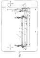
- Fig. 5 is a diagram showing an external appearance of an upper card edge connector, associated with a lower connector 1 according to an embodiment of a card edge connector of the invention which is used with the upper card edge connector as one set.
- Part (a) of Fig. 5 is a plan view and part (b) of Fig. 5 is a right side view.
- the upper card edge connector shown in Fig. 5 can also be used independently from the lower connector.
- the upper card edge connector 3 (hereinafter referred to as the upper connector 3) of the embodiment of the invention will be explained in detail.
- the lower connector 1 has already been explained with reference to Figs. 1 and 2 . Only its interaction with the upper connector 3 will accordingly be explained below.
- the upper connector 3 shown in Fig. 5 is mounted on a parent board M (see Fig. 7 ) which is a printed circuit board, and a child board D2 (see Fig. 7 ), which is a memory module, is attached to the upper connector 3.
- the upper connector 3 includes an insulation housing 31 (hereinafter, referred to housing 31) which receives the child board, plural of contacts 32, a pair of latch arms 33, and pegs 35 which connect the latch arms 33 to the parent board by solder.
- the housing 31 is formed with a slot 311 which receives the child board from front F.
- the contacts 32 are disposed in two, upper and lower, lines extending in the longitudinal direction of the slot 311, i.e., in the lateral direction LR.
- Each contact 32 includes a soldering connection section 32a which is connected to the parent board by soldering.
- Fig. 5 only some of the plural contacts 32 are illustrated and other contacts 32 are not illustrated.
- the pair of latch arms 33 project forward F from both ends of the slot 311 relative to the lateral direction LR.
- the latch arms 33 are formed symmetrically in the lateral direction. The structure of the latch arms 33 will be explained with reference to the latch arm 33 illustrated in detail in the drawings.
- the other latch arm has the same structure.
- the pegs 35 are mounted on the latch arms 33, but to show the shape of the peg 35 better, Fig. 5 shows a state where the peg 35 has been separated from the right latch arm 33.
- the latch arm 33 includes a hold arm 331 which holds the child board, and a support arm 333 which supports the hold arm 331.
- the support arm 333 is formed with a fixed section 334 connected to the parent board through the peg 35 by soldering.
- a folded-back portion 332 which is folded back from the hold arm 331 is provided between the hold arm 331 and the support arm 333.
- a press-fit section 335 which is press-fitted into and fixed to the housing 31, is provided on the same side of the folded back portion 332 as the support arm 333 and at a rear end thereof.
- the latch arm 33 is formed by stamping and bending a metal plate.
- the hold arm 331, the support arm 333, the folded-back portion 332 and the press-fit section 335 are integrally formed.
- the hold arm 331 and the support arm 333 are bifurcated at the folded-back portion 332, and the press-fit section 335, located on the opposite or root side of the bifurcated portion is fixed to the housing 31.
- the hold arm 331 extends forward F from the housing 31.
- the folded-back portion 332 is folded back from an upper edge of a rear end of the hold arm 331 through about 180° toward the outside or away from where the other latch arm 33 at the opposite end of the housing is disposed.
- the support arm 333 extends forward F from the folded-back portion 332.
- the fixed section 334 is provided on a front lower portion of the support arm 333.
- the press-fit section 335 extends backward B from the support arm 333.
- the hold arm 331 is provided at its tip end with a locking piece 331a and a locking piece 331b.
- the locking piece 331a is engaged with a notch formed in an edge of the child board D2 (see Fig. 7 ) to prevent the child board D2 from falling from the housing 31.
- the locking piece 331b keeps the child board in a position parallel to the parent board to maintain electrical connection between the child board and the contact 32.
- the press-fit section 335 is press-fitted into and fixed to the housing 31.
- the hold arm 331 is provided in the form of a cantilever spring in the housing 31 using the press-fit section 335 and the folded-back portion 332 as a base. A tip end of the hold arm 331 displaces in the lateral direction LR by elastic deformation of the hold arm 331 itself.
- the child board D2 When the child board D2 (see Fig. 7 ) is to be attached to the lower connector 1 and the upper connector 3, the child board D2 is first inserted into the slot 311 diagonally with respect to the parent board M (see Fig. 7 ). Then, the hold arm 331 is once elastically deformed outward by manual operation and in this state, the child board D2 is rotated to an angle substantially parallel to the parent board M. Thereby, the child board D2 and the contacts 32 come into contact with each other, and the child board D2 and the parent board M are electrically connected to each other. Then, the hold arms 131 and 231 return inward, and sandwich and hold the child board D2 from both sides in the lateral direction LR by elastic forces. The locking pieces 331a and 331b of the hold arm 331 are engaged with both side edges of the child board.
- Fig. 6 is a perspective view of a base of the latch arm of the upper connector 3 shown in Fig. 5 as viewed from front.
- a long or longitudinal hole or slot 338 which is thin and long in the longitudinal direction FB is formed in the support arm 333 of the latch arm 33 at a substantially central portion thereof in the vertical direction UD.
- the long hole 338 is formed by stamping.
- the long hole 338 corresponds to an example of the cut described in the present invention.
- the support arm 333 is divided by the long hole 338 into an upper first support section 336 and a lower second support section 337.
- the long hole 338 is formed at a location higher than the height of the housing 11 of the lower connector 1 as measured from the position of the parent board.
- the upper first support section 336 is disposed at a position higher than the height of the lower connector 1 (see Fig.
- the folded-back portion 332 is connected to the upper edge rear side of the first support section 336.
- the first support section 336 and the second support section 337 are connected to each other at two locations, i.e., in front F of and behind B the long hole 338.
- the long hole 338 is formed closer to the housing 31 than the front edge 332a of the folded-back portion 332 in the longitudinal direction FB along which the support arm 333 extends.
- the second support section 337 is connected to the first support section at a position closer to the rear end 332b of the folded-back portion 332 in the longitudinal direction FB.
- the first support section 336 is bent outward, i.e., leftward L in Fig. 6 in front F of the front edge 332a of the folded-back portion 332, and the first support section 336 is formed with an inclined portion 336a which is inclined forward F and diagonally outward.
- the first support section 336 is again bent at a position in forward F of the inclined portion 336a and extends forward F substantially parallel to the hold arm 331.
- the first support section 336 is provided at its tip end with stoppers 333c and 333b which prevent the hold arm 331 from bending excessively. Since the hold arm 331 is disposed between the stoppers 333c and 333b provided on the support arm 333 fixed to the parent board, the bending range is limited.
- the second support section 337 is connected to the first support section 336 at a position on the side of the rear edge 332b of the folded-back portion 332.
- the second support section 337 is bent outward, i.e., leftward L at a position below the folded-back portion 332, i.e., at a position where the second support section 337 is superimposed on the folded-back portion 332 in the longitudinal direction FB.
- the second support section 337 is formed with an inclined portion 337a which is inclined forward F and diagonally outward.
- the second support section 337 is again bent at a position in front F of the inclined portion 337a and extends forward F substantially parallel to the hold arm 331, and is connected to the first support section 336. As shown in Fig.
- the fixed section 334 projects from a lower edge of the tip end of the second support section 337.
- the fixed section 334 extends outward from a lower edge at a position where the second support section 337 is connected to the first support section 336.
- the peg 35 which is formed by stamping and bending a metal plate and which has a C-shaped cross-section is mounted on the fixed section 334.
- the peg 35 is connected to the parent board by soldering. When the peg 35 is mounted, the parent board and the upper connector 3 are reliably connected to each other through soldering.
- the fixed sections 334 of the pair of latch arms 33 are disposed at a distance from each other greater than the length of the lower connector 1 in the lateral direction.
- the lower connector 1 can be disposed forward F of the inclined portion 337a of the second support section 337.
- Fig. 7 shows a state where the lower connector 1 and the upper connector 3 are mounted on the parent board.
- Part (a) of Fig. 7 is a plan view and part (b) of Fig. 7 is a right side view.
- Part (b) of Fig. 7 shows a position where the childboards D1 andD2 are mounted, and portions of the connectors are depicted as being see-through so that the positional relationship of the connectors can be easily seen.
- Fig. 8 is an enlarged view of the latch arms of the two connectors shown in Fig. 7 .
- the lower connector 1 and the upper connector 3 are mounted to the surface of the parent board M by soldering.
- the lower connector 1 is disposed between the child board D2 mounted on the upper connector 3 and the parent board M, and is disposed between the pair of latch arms 33 of the upper connector 3. More specifically, the housing 11 of the lower connector 1 is disposed in front F of the inclined portion 337a formed on the latch arm 33 of the upper connector 3.
- the housing 11 of the lower connector 1 is disposed on the back side B, i.e., close to the housing 31 until the housing 11 is arranged beside the folded-back portion 332.
- a disposition distance or spacing W2 between the lower connector 1 and the upper connector 3 is narrower than the disposition distance or spacing W1 between the lower connector 1 and the upper connector 2 shown in Fig. 4 .
- the first support section 336 is bent at a position forward of the front edge 332a (see Fig. 6 ) of the folded-back portion 332, and the length of the folded-back portion 332 is maintained at the same length as that of the folded-back portion 232 of the upper connector 2 shown in Fig. 4 .
- the rigidity of the hold arm 331 is maintained at the same level as that of the hold arm 231 of the upper connector 2 shown in Fig. 4 .
- the folded-back portion 332 has the same strength as that of the upper connector 2 shown in Fig. 4 .
- the example of the upper connector used as a set with a single lower connector is explained, but the invention is not limited to this arrangement.
- the invention may be applied to one of three or more card edge connectors mounted such that three or more child boards are superimposed, except the lowermost card edge connector.
- the card edge connector of the invention is not limited to such an arrangement, and the invention may be applied to a card edge connector for a child board on which an IC expansion function is mounted.
Landscapes
- Coupling Device And Connection With Printed Circuit (AREA)
- Details Of Connecting Devices For Male And Female Coupling (AREA)
Applications Claiming Priority (1)
| Application Number | Priority Date | Filing Date | Title |
|---|---|---|---|
| JP2007119362A JP4852469B2 (ja) | 2007-04-27 | 2007-04-27 | カードエッジコネクタ |
Publications (2)
| Publication Number | Publication Date |
|---|---|
| EP1986276A2 true EP1986276A2 (de) | 2008-10-29 |
| EP1986276A3 EP1986276A3 (de) | 2010-07-14 |
Family
ID=39642889
Family Applications (1)
| Application Number | Title | Priority Date | Filing Date |
|---|---|---|---|
| EP08155028A Withdrawn EP1986276A3 (de) | 2007-04-27 | 2008-04-23 | Kartenrandverbinder |
Country Status (5)
| Country | Link |
|---|---|
| US (1) | US7704090B2 (de) |
| EP (1) | EP1986276A3 (de) |
| JP (1) | JP4852469B2 (de) |
| CN (1) | CN101295840B (de) |
| TW (1) | TWM342662U (de) |
Families Citing this family (2)
| Publication number | Priority date | Publication date | Assignee | Title |
|---|---|---|---|---|
| US9335797B1 (en) | 2014-05-01 | 2016-05-10 | Google Inc. | Supporting computer boards |
| US20210315121A1 (en) * | 2018-08-02 | 2021-10-07 | Samtec, Inc. | Transceiver latch and thermal bridge |
Citations (2)
| Publication number | Priority date | Publication date | Assignee | Title |
|---|---|---|---|---|
| US6126472A (en) | 1995-02-24 | 2000-10-03 | Hon Hai Precision Ind. Co., Ltd. | Duplex profile connector assembly |
| JP2002190354A (ja) | 2000-12-21 | 2002-07-05 | Tyco Electronics Amp Kk | カードエッジコネクタ |
Family Cites Families (10)
| Publication number | Priority date | Publication date | Assignee | Title |
|---|---|---|---|---|
| JP3768263B2 (ja) * | 1995-06-15 | 2006-04-19 | タイコエレクトロニクスアンプ株式会社 | エッジコネクタ |
| US5839913A (en) * | 1995-06-15 | 1998-11-24 | The Whitaker Corporation | Edge connector having latches for multiple daughter boards |
| US6027357A (en) * | 1996-12-13 | 2000-02-22 | The Whitaker Corporation | Electrical connector having metal latch |
| TW361710U (en) * | 1997-10-21 | 1999-06-11 | Hon Hai Prec Ind Co Ltd | Power connector |
| JP2000208183A (ja) * | 1998-07-27 | 2000-07-28 | Tyco Electronics Amp Kk | カ―ドエッジコネクタ |
| JP2000294320A (ja) * | 1999-04-09 | 2000-10-20 | Nagase & Co Ltd | 印刷配線板コネクタ |
| TW407809U (en) * | 1999-04-23 | 2000-10-01 | Ind Tech Res Inst | Latch locking mechanism for slant inserting type PCB connector |
| CN2539301Y (zh) * | 2002-03-12 | 2003-03-05 | 莫列斯公司 | 卡缘连接器 |
| US6743028B2 (en) * | 2002-09-16 | 2004-06-01 | Speed Tech Corp. | Electrical connector for attaching a circuit board |
| US6796825B2 (en) * | 2002-10-17 | 2004-09-28 | Speed Tech Corp. | Electrical connector for attaching a circuit board |
-
2007
- 2007-04-27 JP JP2007119362A patent/JP4852469B2/ja not_active Expired - Fee Related
-
2008
- 2008-03-11 TW TW097204100U patent/TWM342662U/zh not_active IP Right Cessation
- 2008-04-18 US US12/105,432 patent/US7704090B2/en not_active Expired - Fee Related
- 2008-04-23 EP EP08155028A patent/EP1986276A3/de not_active Withdrawn
- 2008-04-25 CN CN2008100959446A patent/CN101295840B/zh not_active Expired - Fee Related
Patent Citations (2)
| Publication number | Priority date | Publication date | Assignee | Title |
|---|---|---|---|---|
| US6126472A (en) | 1995-02-24 | 2000-10-03 | Hon Hai Precision Ind. Co., Ltd. | Duplex profile connector assembly |
| JP2002190354A (ja) | 2000-12-21 | 2002-07-05 | Tyco Electronics Amp Kk | カードエッジコネクタ |
Also Published As
| Publication number | Publication date |
|---|---|
| EP1986276A3 (de) | 2010-07-14 |
| CN101295840A (zh) | 2008-10-29 |
| US20080268688A1 (en) | 2008-10-30 |
| US7704090B2 (en) | 2010-04-27 |
| TWM342662U (en) | 2008-10-11 |
| JP4852469B2 (ja) | 2012-01-11 |
| CN101295840B (zh) | 2011-12-21 |
| JP2008277124A (ja) | 2008-11-13 |
Similar Documents
| Publication | Publication Date | Title |
|---|---|---|
| US7131875B2 (en) | Contact and electrical connector | |
| US7575487B2 (en) | Electric connector | |
| US8979551B2 (en) | Low-profile mezzanine connector | |
| US8460034B2 (en) | Miniature electrical connector | |
| KR101982747B1 (ko) | 콤팩트 고속 커넥터 | |
| US10381776B2 (en) | Connector assembly with an improved latch member having a shorter length | |
| KR101105965B1 (ko) | 콘택트 및 전기커넥터 | |
| JP2001203027A (ja) | 直交接触アームおよびオフセット接触領域を備えた電気コンタクト | |
| JP2007149394A (ja) | コネクタ | |
| US7059907B2 (en) | Modular electrical connector | |
| CN106575831A (zh) | 连接器以及在该连接器中使用的插头及插口 | |
| WO2010135540A1 (en) | Board-to-board connector | |
| JP3134262U (ja) | 表面実装型コネクタ | |
| CN101490907B (zh) | 电缆连接器 | |
| US12136780B2 (en) | Connector comprising a terminal with an arm having a base portion extending alongside a contact poriton | |
| US7637778B2 (en) | Board-mounted type connector to which a shield plate is attached | |
| WO1998054799A1 (en) | Card edge connector and contact | |
| EP1416590B1 (de) | Verbinder mit effektivem Abstandhalteraum | |
| US6979219B2 (en) | Zero insertion force dual beam surface mount contact | |
| EP1986276A2 (de) | Kartenrandverbinder | |
| JP2002050420A (ja) | 基板用コネクタ | |
| CN2458772Y (zh) | 电连接器 | |
| US20260045713A1 (en) | High performance interposer | |
| EP4601127A1 (de) | Schwimmender verbinder und gegenverbinder dafür | |
| JP2009277372A (ja) | 雌コネクタとコネクタ接続構造 |
Legal Events
| Date | Code | Title | Description |
|---|---|---|---|
| PUAI | Public reference made under article 153(3) epc to a published international application that has entered the european phase |
Free format text: ORIGINAL CODE: 0009012 |
|
| AK | Designated contracting states |
Kind code of ref document: A2 Designated state(s): AT BE BG CH CY CZ DE DK EE ES FI FR GB GR HR HU IE IS IT LI LT LU LV MC MT NL NO PL PT RO SE SI SK TR |
|
| AX | Request for extension of the european patent |
Extension state: AL BA MK RS |
|
| RAP1 | Party data changed (applicant data changed or rights of an application transferred) |
Owner name: TYCO ELECTRONICS JAPAN G.K. |
|
| PUAL | Search report despatched |
Free format text: ORIGINAL CODE: 0009013 |
|
| AK | Designated contracting states |
Kind code of ref document: A3 Designated state(s): AT BE BG CH CY CZ DE DK EE ES FI FR GB GR HR HU IE IS IT LI LT LU LV MC MT NL NO PL PT RO SE SI SK TR |
|
| AX | Request for extension of the european patent |
Extension state: AL BA MK RS |
|
| AKY | No designation fees paid | ||
| REG | Reference to a national code |
Ref country code: DE Ref legal event code: R108 Effective date: 20110222 Ref country code: DE Ref legal event code: 8566 |
|
| STAA | Information on the status of an ep patent application or granted ep patent |
Free format text: STATUS: THE APPLICATION IS DEEMED TO BE WITHDRAWN |
|
| 18D | Application deemed to be withdrawn |
Effective date: 20110115 |