EP1980899A2 - Anzeigevorrichtung mit doppelbrechendem Substrat - Google Patents
Anzeigevorrichtung mit doppelbrechendem Substrat Download PDFInfo
- Publication number
- EP1980899A2 EP1980899A2 EP08159644A EP08159644A EP1980899A2 EP 1980899 A2 EP1980899 A2 EP 1980899A2 EP 08159644 A EP08159644 A EP 08159644A EP 08159644 A EP08159644 A EP 08159644A EP 1980899 A2 EP1980899 A2 EP 1980899A2
- Authority
- EP
- European Patent Office
- Prior art keywords
- polarizer
- optically active
- substrate
- display device
- layer
- Prior art date
- Legal status (The legal status is an assumption and is not a legal conclusion. Google has not performed a legal analysis and makes no representation as to the accuracy of the status listed.)
- Granted
Links
Images
Classifications
-
- G—PHYSICS
- G02—OPTICS
- G02F—OPTICAL DEVICES OR ARRANGEMENTS FOR THE CONTROL OF LIGHT BY MODIFICATION OF THE OPTICAL PROPERTIES OF THE MEDIA OF THE ELEMENTS INVOLVED THEREIN; NON-LINEAR OPTICS; FREQUENCY-CHANGING OF LIGHT; OPTICAL LOGIC ELEMENTS; OPTICAL ANALOGUE/DIGITAL CONVERTERS
- G02F1/00—Devices or arrangements for the control of the intensity, colour, phase, polarisation or direction of light arriving from an independent light source, e.g. switching, gating or modulating; Non-linear optics
- G02F1/01—Devices or arrangements for the control of the intensity, colour, phase, polarisation or direction of light arriving from an independent light source, e.g. switching, gating or modulating; Non-linear optics for the control of the intensity, phase, polarisation or colour
- G02F1/13—Devices or arrangements for the control of the intensity, colour, phase, polarisation or direction of light arriving from an independent light source, e.g. switching, gating or modulating; Non-linear optics for the control of the intensity, phase, polarisation or colour based on liquid crystals, e.g. single liquid crystal display cells
- G02F1/133—Constructional arrangements; Operation of liquid crystal cells; Circuit arrangements
- G02F1/1333—Constructional arrangements; Manufacturing methods
- G02F1/1335—Structural association of cells with optical devices, e.g. polarisers or reflectors
- G02F1/133528—Polarisers
-
- G—PHYSICS
- G02—OPTICS
- G02F—OPTICAL DEVICES OR ARRANGEMENTS FOR THE CONTROL OF LIGHT BY MODIFICATION OF THE OPTICAL PROPERTIES OF THE MEDIA OF THE ELEMENTS INVOLVED THEREIN; NON-LINEAR OPTICS; FREQUENCY-CHANGING OF LIGHT; OPTICAL LOGIC ELEMENTS; OPTICAL ANALOGUE/DIGITAL CONVERTERS
- G02F1/00—Devices or arrangements for the control of the intensity, colour, phase, polarisation or direction of light arriving from an independent light source, e.g. switching, gating or modulating; Non-linear optics
- G02F1/01—Devices or arrangements for the control of the intensity, colour, phase, polarisation or direction of light arriving from an independent light source, e.g. switching, gating or modulating; Non-linear optics for the control of the intensity, phase, polarisation or colour
- G02F1/13—Devices or arrangements for the control of the intensity, colour, phase, polarisation or direction of light arriving from an independent light source, e.g. switching, gating or modulating; Non-linear optics for the control of the intensity, phase, polarisation or colour based on liquid crystals, e.g. single liquid crystal display cells
- G02F1/133—Constructional arrangements; Operation of liquid crystal cells; Circuit arrangements
- G02F1/1333—Constructional arrangements; Manufacturing methods
- G02F1/133305—Flexible substrates, e.g. plastics, organic film
-
- G—PHYSICS
- G02—OPTICS
- G02F—OPTICAL DEVICES OR ARRANGEMENTS FOR THE CONTROL OF LIGHT BY MODIFICATION OF THE OPTICAL PROPERTIES OF THE MEDIA OF THE ELEMENTS INVOLVED THEREIN; NON-LINEAR OPTICS; FREQUENCY-CHANGING OF LIGHT; OPTICAL LOGIC ELEMENTS; OPTICAL ANALOGUE/DIGITAL CONVERTERS
- G02F1/00—Devices or arrangements for the control of the intensity, colour, phase, polarisation or direction of light arriving from an independent light source, e.g. switching, gating or modulating; Non-linear optics
- G02F1/01—Devices or arrangements for the control of the intensity, colour, phase, polarisation or direction of light arriving from an independent light source, e.g. switching, gating or modulating; Non-linear optics for the control of the intensity, phase, polarisation or colour
- G02F1/13—Devices or arrangements for the control of the intensity, colour, phase, polarisation or direction of light arriving from an independent light source, e.g. switching, gating or modulating; Non-linear optics for the control of the intensity, phase, polarisation or colour based on liquid crystals, e.g. single liquid crystal display cells
- G02F1/133—Constructional arrangements; Operation of liquid crystal cells; Circuit arrangements
- G02F1/1333—Constructional arrangements; Manufacturing methods
- G02F1/1335—Structural association of cells with optical devices, e.g. polarisers or reflectors
- G02F1/133528—Polarisers
- G02F1/133543—Cholesteric polarisers
-
- G—PHYSICS
- G02—OPTICS
- G02F—OPTICAL DEVICES OR ARRANGEMENTS FOR THE CONTROL OF LIGHT BY MODIFICATION OF THE OPTICAL PROPERTIES OF THE MEDIA OF THE ELEMENTS INVOLVED THEREIN; NON-LINEAR OPTICS; FREQUENCY-CHANGING OF LIGHT; OPTICAL LOGIC ELEMENTS; OPTICAL ANALOGUE/DIGITAL CONVERTERS
- G02F1/00—Devices or arrangements for the control of the intensity, colour, phase, polarisation or direction of light arriving from an independent light source, e.g. switching, gating or modulating; Non-linear optics
- G02F1/01—Devices or arrangements for the control of the intensity, colour, phase, polarisation or direction of light arriving from an independent light source, e.g. switching, gating or modulating; Non-linear optics for the control of the intensity, phase, polarisation or colour
- G02F1/13—Devices or arrangements for the control of the intensity, colour, phase, polarisation or direction of light arriving from an independent light source, e.g. switching, gating or modulating; Non-linear optics for the control of the intensity, phase, polarisation or colour based on liquid crystals, e.g. single liquid crystal display cells
- G02F1/133—Constructional arrangements; Operation of liquid crystal cells; Circuit arrangements
- G02F1/1333—Constructional arrangements; Manufacturing methods
- G02F1/1335—Structural association of cells with optical devices, e.g. polarisers or reflectors
- G02F1/133528—Polarisers
- G02F1/133548—Wire-grid polarisers
-
- G—PHYSICS
- G02—OPTICS
- G02F—OPTICAL DEVICES OR ARRANGEMENTS FOR THE CONTROL OF LIGHT BY MODIFICATION OF THE OPTICAL PROPERTIES OF THE MEDIA OF THE ELEMENTS INVOLVED THEREIN; NON-LINEAR OPTICS; FREQUENCY-CHANGING OF LIGHT; OPTICAL LOGIC ELEMENTS; OPTICAL ANALOGUE/DIGITAL CONVERTERS
- G02F1/00—Devices or arrangements for the control of the intensity, colour, phase, polarisation or direction of light arriving from an independent light source, e.g. switching, gating or modulating; Non-linear optics
- G02F1/01—Devices or arrangements for the control of the intensity, colour, phase, polarisation or direction of light arriving from an independent light source, e.g. switching, gating or modulating; Non-linear optics for the control of the intensity, phase, polarisation or colour
- G02F1/13—Devices or arrangements for the control of the intensity, colour, phase, polarisation or direction of light arriving from an independent light source, e.g. switching, gating or modulating; Non-linear optics for the control of the intensity, phase, polarisation or colour based on liquid crystals, e.g. single liquid crystal display cells
- G02F1/133—Constructional arrangements; Operation of liquid crystal cells; Circuit arrangements
- G02F1/1333—Constructional arrangements; Manufacturing methods
- G02F1/1335—Structural association of cells with optical devices, e.g. polarisers or reflectors
- G02F1/13356—Structural association of cells with optical devices, e.g. polarisers or reflectors characterised by the placement of the optical elements
- G02F1/133565—Structural association of cells with optical devices, e.g. polarisers or reflectors characterised by the placement of the optical elements inside the LC elements, i.e. between the cell substrates
-
- G—PHYSICS
- G02—OPTICS
- G02F—OPTICAL DEVICES OR ARRANGEMENTS FOR THE CONTROL OF LIGHT BY MODIFICATION OF THE OPTICAL PROPERTIES OF THE MEDIA OF THE ELEMENTS INVOLVED THEREIN; NON-LINEAR OPTICS; FREQUENCY-CHANGING OF LIGHT; OPTICAL LOGIC ELEMENTS; OPTICAL ANALOGUE/DIGITAL CONVERTERS
- G02F1/00—Devices or arrangements for the control of the intensity, colour, phase, polarisation or direction of light arriving from an independent light source, e.g. switching, gating or modulating; Non-linear optics
- G02F1/01—Devices or arrangements for the control of the intensity, colour, phase, polarisation or direction of light arriving from an independent light source, e.g. switching, gating or modulating; Non-linear optics for the control of the intensity, phase, polarisation or colour
- G02F1/13—Devices or arrangements for the control of the intensity, colour, phase, polarisation or direction of light arriving from an independent light source, e.g. switching, gating or modulating; Non-linear optics for the control of the intensity, phase, polarisation or colour based on liquid crystals, e.g. single liquid crystal display cells
- G02F1/133—Constructional arrangements; Operation of liquid crystal cells; Circuit arrangements
- G02F1/1333—Constructional arrangements; Manufacturing methods
- G02F1/1335—Structural association of cells with optical devices, e.g. polarisers or reflectors
- G02F1/13363—Birefringent elements, e.g. for optical compensation
Definitions
- the present invention relates to display devices comprising at least one substrate, a first and a second electrode, a display medium and an optically active layer, as well as to methods for the production thereof.
- Display devices such as liquid crystal displays (LCDs) and light emitting diode displays (LED-displays) are complex devices.
- display devices In addition to the display medium, i.e. the liquid crystal layer forming the optical switch in LCDs and the electroluminiscent layer in LED-displays, display devices further comprise a large number of separate films and layers with various functions, such as display substrates and optically active components, such as polarizers, retarders, diffusers, reflectors, transflectors and color filters etc.
- optically active components are laminated on the exterior of the display substrates.
- the actual optical active components are usually sandwiched between protective sheets or applied onto a carrier sheet.
- adhesive layers are required in order to laminate the layers onto the display substrate. Through the use of these additional layers, each component adds ⁇ 100 ⁇ m on the display thickness.
- the intrinsic flexibility of displays that are based on polymer substrates is limited by the use of passive optical films with a thickness of ⁇ 100 ⁇ m each, as the bending stiffness of the display scales with the third power of the thickness.
- display device applications such as LCDs using polarization optics for image formation, (such as twisted nematic, super-twisted nematic, in plane switching, vertically aligned nematic, optically compensated birefringence and ferro-electric LCDs) and polyLED-displays using a combination of a retarder and a polarizer for daylight contrast enhancement, require that the display substrates are isotropic, since birefringence in the substrate would impair the optical performance of the display as the polarization of light changes while traveling through a birefringent substrate.
- US patent no 6 151 088 proposes a liquid crystal display based on polymeric birefringent display substrates.
- a display according to the '088-patent requires that several requirements regarding angles between the polarizer axis, the optical axis of the substrate and the direction of the liquid crystal molecules in the middle portion of the liquid crystal layer. Furthermore the retardation value of suitable substrates is strictly limited.
- a display device according to the '088-patent is also bound to be unsuitably thick for flexible displays, as polarizers and other optical components are laminated on the outside of the substrate in the same manner as described above.
- the present invention thus provides a display device comprising at least one substrate, a first and a second electrode, a display medium and an optically active layer, which is characterized in that said optically active layer comprises a polarizer and is arranged between said substrate and said display medium, and wherein said substrate is made of a birefringent material.
- birefringent substrate and "birefringent material” refers to, in addition to the conventional meaning of a substrate or a material which exhibits birefringence, also substrates and materials for use in display devices that may become birefringent under some conditions of normal use for the display device.
- non-birefringent or essentially non-birefringent materials that becomes birefringent when a strain is applied on them, such as when they are being bent, are also encompassed by the meaning of the terms "birefringent substrate” and "birefringent material”.
- the term "display medium” relates to the active component in the display capable of image formation, i.e. the switching liquid crystal layer in a LCD and the electroluminiscent layer in a polyLED-display or an OLED-display.
- optically active layer and “optically active components” refer to layers/components that affect properties, such as polarization, ellipticity, color spectrum, propagation direction, etc, of light passing through such layers/components.
- An optically active layer may comprise one or more optically active components, sub-layers, forming the optically active unit(s) of said layer.
- An optically active layer may also, in addition to optically active components, comprise optically non-active components (e.g. sub-layers), such as components necessary for the formation of the optically active components, for example alignment films, or protective films protecting the optically active layer from degradation, such as a film that protects an optically active layer from chemical degradation during e.g. ITO-structuring steps.
- a polarizer is conventionally positioned between the liquid crystal layer and the end user.
- One object of such a polarizer is to block light from entering into or exiting from the display unless this light has such a polarization that it is not absorbed by the polarizer.
- the polarizer is arranged between the substrate and the display medium.
- light exiting from the display towards the user will pass the polarizer before passing through the birefringent substrate.
- light entering a display device of the invention will pass the polarizer after having traveled through the substrate. Changes in polarization of the light that takes place in the substrate does not impair the action of the polarizer and thus, in a display device according to the present invention, the birefringence of the substrate will not impair the optical properties of the display device.
- polarizers and optionally other optically active components, are located on the inside of the device, thus being protected from environmental influence, such as scratches, humidity and dust. This allows for the construction of thinner displays since the conventional protection layers applied on the outside of the optically active components (if arranged on the outside of the device) may be omitted.
- display devices may be produced that are cheaper, since birefringent substrates may be produced more economically than non-birefringent substrates.
- the substrate may be flexible.
- Flexible substrates allows for the production of flexible displays, which is highly desired in many present and anticipated applications.
- the substrate may be of a polymeric material, e.g. consisting of polyethyleneterephtalate, polyethylenenaphtalate, polycarbonate, polynorbornene, polyethersulphone, polyimide, polyethylene or any suitable combination of two or more thereof.
- a polymeric material e.g. consisting of polyethyleneterephtalate, polyethylenenaphtalate, polycarbonate, polynorbornene, polyethersulphone, polyimide, polyethylene or any suitable combination of two or more thereof.
- Other polymeric materials suitable for use in a display device according to the present will be apparent to those skilled in the art.
- Polymeric birefringent materials are conventionally easier and less costly to produce than polymeric non-birefringent materials.
- a polymeric birefringent substrate according to the present invention can be manufactured by melt-extrusion, solvent casting or other methods known to those skilled in the art.
- the retardation of the substrate may be greater than 10 nm, for example greater than 50 nm or greater than 100 nm, under the conditions in which the display is used.
- Any suitable polarizer may be used in a display device according the present invention.
- a suitable polarizer comprises a crystallized layer of parallel aligned columnar stacks of lyotropic dyes, such as lyotropic perylene dyes (e.g. as available from Optiva).
- lyotropic dyes such as lyotropic perylene dyes (e.g. as available from Optiva).
- Such a polarizer may be coated, e.g. doctor blade coated, on a substrate as a volatile solution, in which the dyes form columnar stacks. During the coating, the dye stacks is oriented on the substrate by shear force. The solvent is evaporated, and leaves a thin polarizing film (E-type polarizer) on the substrate.
- E-type polarizer thin polarizing film
- Such a polarizer may be produced very thin (as thin as ⁇ 1 ⁇ m).
- Another polarizer suitable for use in the present display device is a polarizer comprising dichroic dyes incorporated in a polymerized mixture of aligned mesogens or polymers of mesogens.
- a polymerizable mixture of mesogens or polymers of mesogens, capable of forming a ordered phase, such as a nematic or smectic phase, is applied and aligned on a substrate. After alignment of the mixture on the substrate, the ordered phase is obtained in the mixture, which is then polymerized.
- the mixture is capable of forming a highly ordered phase, such as a smectic phase, e.g.
- the smectic phase is preferably obtained in the mixture before polymerization.
- the dichroic dyes becomes fixed in and oriented by the polymerized layer.
- the polymerized layer becomes a polarizer.
- a polarizer may also be formed by attaching dyes to polymers of mesogens, such as a side chain on or comprised in polymers of mesogens, which may be aligned in the LC-phase above the glass transition temperature.
- Still another polarizer suitable for use in the present display device is a wideband circular polarizer based on a cholesteric material in which there is a gradient in the helical pitch over the thickness of the cholesteric film.
- Yet another type of polarizer suitable for use in the present display device comprises a grid of plane parallel metal wires (e.g. as available from Moxtek).
- the grid is thin, e.g. about 100-200 nm thick.
- a grid pitch in the order of about 150 nm is suitable to polarize visible light.
- any polarizer suitable for use in a display device according to the present invention may be used.
- An optically active layer of the present invention may further comprise optically active components, such as polarizers, retarders, transflectors, color filters, in-cell diffusers, reflectors, scattering films and other optically active components known to those skilled in the art.
- optically active components such as polarizers, retarders, transflectors, color filters, in-cell diffusers, reflectors, scattering films and other optically active components known to those skilled in the art.
- optical components are known to those skilled in the art as optical components necessary for the function of a display device or components improving the performance of the display device.
- the type, number and arrangement of such optically active components varies with the type of display device, and is known to those skilled in the art.
- optically active components such as polarizers and retarders
- Such strain may occur when the display device is bent, wherein an elongation occurs on the convex part of the bent display and a compression occurs on the concave side of the bent display.
- a neutral line exists, often near the center of the display, where essentially no such strain, i.e. elongation or compression, occurs.
- retarders suitable for use in an optically active layer in a display device of the present invention may be used.
- Such retarders include, but are not limited to, ⁇ /4-retarders, wide band ⁇ /4-retarders, ⁇ /2-retarters, etc.
- a retarder suitable for use in a display device is a film formed by aligning a polymerizable mixture of reactive mesogens or LC-monomers on a surface, such as a substrate, optionally provided with an additional film, such as an optically active component, e.g. a polarizer disposed on said substrate, provided with a alignment layer, such as a rubbed polyimide film or a photoalignment layer.
- a preferred order is then achieved in the mesogen mixture, e.g. by heating to a selected temperature or by other known methods for achieving a preferred order.
- the mixture is then polymerized to fix the achieved order, resulting in a thin birefringent film exhibiting a good stability.
- Optically active components in an optically active layer in a display device of the present invention may be patterned, i.e. that the optically active component comprises at least one domain in which the optical properties are different from the optical properties in another domain of the optically active component.
- patterned optically active components such as patterned retarders
- patterned optically active components are arranged near the display medium, thus reducing parallax problems which occurs when the distance between the optically active component(s) and the display medium is larger, e.g. separated by the substrate.
- the display medium may comprise a liquid crystal layer to form a LCD-display, such as, but not limited to those using polarization optics for image formation, for example twisted nematic, vertically aligned, super-twisted nematic and ferroelectric liquid crystal displays.
- Liquid crystal displays, LCDs, according to the present invention comprise both displays comprising one substrate, such as stratified LCDs, and displays comprising two substrates sandwiching the display medium.
- LCDs according to the present invention comprising two substrates may comprise a first and a second substrate, of which at least one substrate is birefringent. Further, first and second optically active layers are arranged between said front and back substrates, first and a second electrodes are arranged between said first and second optically active layers, and a liquid crystal layer is arranged between said electrodes, wherein at least said first optically active layer comprises a polarizing layer.
- LCDs according to the present invention comprise displays as transmissive, reflective and transflective displays.
- the arrangement of the optically active layer(s) in different types of LCDs are known to those skilled in the art.
- the display medium comprises an electroluminiscent layer, i.e. a polyLED- or an OLED-display, especially such polyLED or OLED-displays using a combination of a retarder, e.g. a ⁇ /4-retarder, and a polarizer as a daylight contrast enhancement layer.
- a polyLED- or OLED display may comprise a polarizer arranged on a birefringent substrate, a retarder arranged on the polarizer and a polyLED- or OLED-assembly arranged on the substrate with the retarder facing the light transmitting side of the polyLED- or OLED-assembly.
- the birefringent substrate, the polarizer and the retarder may be any suitable substrate, polarizer and retarder, respectively, for example any of those described above.
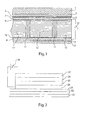
- a first embodiment of the present invention is a LCD-display comprising a front substrate 1 and a back substrate 2, both made of a birefringent polymeric material.
- a front polarizer 3 and a back polarizer 4 are arranged on said front substrate 1 and back substrate 2 respectively.
- Both the polarizers comprise a dried film of columnar stacks of perylene dyes, forming E-type polarizers on the surface of the substrate.
- a retarder 5 is arranged on the front polarizer 3.
- the retarder is a polymerized mesogen layer and is aligned on an alignment layer 6 disposed on the polarizer.
- a first patterned electrode, a conductive patterned ITO-layer, 7 is arranged on the retarder 5 and a second patterned electrode 8 is arranged on the back polarizer 4.
- Alignment layers of rubbed polyimide 9 and 10 are arranged on the electrodes 7 and 8 respectively, and spacers 11 are lithographically disposed on the alignment layer 10.
- the two substrates are coupled to each other, with the alignment layers 9 and 10 facing each other, and the void between the alignment layers 9 and 10 is filled with a liquid crystal material 12.
- the electrodes 7 and 8 are connected to a control unit 13, which controls the electrodes, which in turn controls the orientation of the liquid crystal molecules in the liquid crystal material 12 between the electrodes, thus determining the image to be displayed.
- Light entering the display either through the back substrate or the front substrate passes through the back or front polarizers respectively after having passed the birefringent substrate.
- light entering the LC-layer will have the desired polarization independent of the birefringence of the substrate.
- light exiting the LC-layer passes the polarizer before being affected by the birefringence of the substrate.
- the front and back substrates may be made of the same or ' different materials, and one of the substrates may be non-birefringent.
- the front and back polarizers may be the same or different and may be independently chosen among all polarizers suitable for use in display device according to the present invention.
- the retarder may be a patterned or a non-patterned retarder, and may be any retarder suitable for use in a display device according to the present invention.
- the display device may further comprise additional components, such as color filters for a color display, etc..
- the electrodes are not necessarily ITO-electrodes. Other electrodes known by those skilled in the art may be used.
- a second exemplary embodiment of the present invention is a polyLED-display equipped with a daylight contrast enhancement layer. It comprises a polymeric birefringent substrate 21, a polarizer 22 arranged on said substrate and a ⁇ /4-retarder 23 arranged on said polarizer.
- a polyLED-assembly comprising of an ITO-anode 24 and a cathode 25 sandwiching a light emitting polymer 26 and a PEDOT (polyethylenedioxythiophene) layer 27, is arranged.
- the anode 24 and the cathode 25 are connected to a control unit 28, which thus controls the light emission from the light emitting polymer 26, thus determining the image to be displayed.
Landscapes
- Physics & Mathematics (AREA)
- Nonlinear Science (AREA)
- Optics & Photonics (AREA)
- Crystallography & Structural Chemistry (AREA)
- Chemical & Material Sciences (AREA)
- General Physics & Mathematics (AREA)
- Mathematical Physics (AREA)
- Electroluminescent Light Sources (AREA)
- Devices For Indicating Variable Information By Combining Individual Elements (AREA)
- Polarising Elements (AREA)
- Liquid Crystal (AREA)
- Holo Graphy (AREA)
- Display Devices Of Pinball Game Machines (AREA)
Priority Applications (2)
| Application Number | Priority Date | Filing Date | Title |
|---|---|---|---|
| EP08159644A EP1980899B1 (de) | 2004-09-03 | 2005-08-25 | Anzeigevorrichtung mit doppelbrechendem Substrat |
| PL08159644T PL1980899T3 (pl) | 2004-09-03 | 2005-08-25 | Urządzenie wyświetlające z dwójłomnym podłożem |
Applications Claiming Priority (3)
| Application Number | Priority Date | Filing Date | Title |
|---|---|---|---|
| EP04104271 | 2004-09-03 | ||
| EP08159644A EP1980899B1 (de) | 2004-09-03 | 2005-08-25 | Anzeigevorrichtung mit doppelbrechendem Substrat |
| EP05781263A EP1789838B1 (de) | 2004-09-03 | 2005-08-25 | Anzeigevorrichtung mit doppelbrechender schicht |
Related Parent Applications (2)
| Application Number | Title | Priority Date | Filing Date |
|---|---|---|---|
| EP05781263A Division EP1789838B1 (de) | 2004-09-03 | 2005-08-25 | Anzeigevorrichtung mit doppelbrechender schicht |
| EP05781263.8 Division | 2005-08-25 |
Publications (3)
| Publication Number | Publication Date |
|---|---|
| EP1980899A2 true EP1980899A2 (de) | 2008-10-15 |
| EP1980899A3 EP1980899A3 (de) | 2008-10-29 |
| EP1980899B1 EP1980899B1 (de) | 2010-06-30 |
Family
ID=35219507
Family Applications (2)
| Application Number | Title | Priority Date | Filing Date |
|---|---|---|---|
| EP08159644A Expired - Lifetime EP1980899B1 (de) | 2004-09-03 | 2005-08-25 | Anzeigevorrichtung mit doppelbrechendem Substrat |
| EP05781263A Expired - Lifetime EP1789838B1 (de) | 2004-09-03 | 2005-08-25 | Anzeigevorrichtung mit doppelbrechender schicht |
Family Applications After (1)
| Application Number | Title | Priority Date | Filing Date |
|---|---|---|---|
| EP05781263A Expired - Lifetime EP1789838B1 (de) | 2004-09-03 | 2005-08-25 | Anzeigevorrichtung mit doppelbrechender schicht |
Country Status (10)
| Country | Link |
|---|---|
| US (1) | US7671520B2 (de) |
| EP (2) | EP1980899B1 (de) |
| JP (1) | JP2008511854A (de) |
| KR (1) | KR20070059073A (de) |
| CN (1) | CN101010622B (de) |
| AT (2) | ATE472747T1 (de) |
| DE (2) | DE602005009724D1 (de) |
| PL (2) | PL1789838T3 (de) |
| TW (1) | TW200619786A (de) |
| WO (1) | WO2006025002A1 (de) |
Cited By (2)
| Publication number | Priority date | Publication date | Assignee | Title |
|---|---|---|---|---|
| EP2555044A1 (de) * | 2011-08-03 | 2013-02-06 | Samsung Electronics Co., Ltd. | Anzeigetafel und Anzeigevorrichtung damit |
| EP2648034A1 (de) * | 2012-04-03 | 2013-10-09 | Samsung Electronics Co., Ltd. | Anzeigetafel und damit versehene Anzeigevorrichtung |
Families Citing this family (13)
| Publication number | Priority date | Publication date | Assignee | Title |
|---|---|---|---|---|
| US7751006B2 (en) * | 2006-09-29 | 2010-07-06 | Dai Nippon Printing Co., Ltd. | Optical element, liquid crystal display device member with the optical element, liquid crystal display device with the liquid crystal display device member, method of producing the optical element and method of evaluating birefringence functional layer |
| JP5671449B2 (ja) * | 2008-04-23 | 2015-02-18 | レイブンブリック,エルエルシー | 反射性表面およびサーモリフレクティブ表面についてのグレアを調整する方法および装置 |
| KR101142674B1 (ko) | 2009-09-09 | 2012-05-10 | 광운대학교 산학협력단 | 유연성 있는 gbo 반사 편광 기판상에 제작된 편광 발광성 유기 발광 소자 |
| WO2011125390A1 (ja) * | 2010-04-02 | 2011-10-13 | コニカミノルタホールディングス株式会社 | 有機発光素子 |
| US8796704B2 (en) * | 2011-05-02 | 2014-08-05 | Innolux Corporation | Emissive display having polarizer and retarder films |
| US8525405B2 (en) * | 2011-08-19 | 2013-09-03 | Apple Inc. | Electronic devices with flexible glass polarizers |
| JP5685558B2 (ja) * | 2012-04-19 | 2015-03-18 | 株式会社東芝 | 表示装置 |
| CN102830534A (zh) * | 2012-08-23 | 2012-12-19 | 京东方科技集团股份有限公司 | 彩膜基板、阵列基板、液晶显示装置及其制作方法 |
| US9761843B2 (en) | 2012-11-30 | 2017-09-12 | 3M Innovative Properties Company | Emissive display with hybrid polarizer |
| KR20160120837A (ko) * | 2015-04-08 | 2016-10-19 | 삼성디스플레이 주식회사 | 액정 표시 장치 |
| JP2017090543A (ja) * | 2015-11-04 | 2017-05-25 | 株式会社ポラテクノ | 液晶表示装置 |
| KR102079133B1 (ko) * | 2015-12-22 | 2020-02-19 | 주식회사 엘지화학 | 디스플레이 장치용 기판 |
| KR102853077B1 (ko) | 2020-09-09 | 2025-09-01 | (주)엘엑스하우시스 | 디스플레이 장치용 윈도우 커버의 제조 방법 및 디스플레이 장치용 윈도우 커버 |
Citations (1)
| Publication number | Priority date | Publication date | Assignee | Title |
|---|---|---|---|---|
| US6151088A (en) | 1996-08-27 | 2000-11-21 | Ricoh Co., Ltd. | Liquid crystal display apparatus |
Family Cites Families (33)
| Publication number | Priority date | Publication date | Assignee | Title |
|---|---|---|---|---|
| JPS5348498A (en) * | 1976-10-14 | 1978-05-01 | Seiko Epson Corp | Display device |
| JPS5436442U (de) * | 1977-08-17 | 1979-03-09 | ||
| US4181756A (en) * | 1977-10-05 | 1980-01-01 | Fergason James L | Process for increasing display brightness of liquid crystal displays by bleaching polarizers using screen-printing techniques |
| JPS5887538A (ja) * | 1981-11-20 | 1983-05-25 | Hitachi Ltd | 液晶表示素子 |
| JPS5995513A (ja) | 1982-11-25 | 1984-06-01 | Toray Ind Inc | 液晶表示セル |
| US4674840A (en) * | 1983-12-22 | 1987-06-23 | Polaroid Corporation, Patent Dept. | Liquid crystal display with polarizer and biaxial birefringent support |
| JPS61156027A (ja) * | 1984-12-27 | 1986-07-15 | Nissha Printing Co Ltd | カラ−液晶表示装置 |
| US4688897A (en) * | 1985-06-17 | 1987-08-25 | Hughes Aircraft Company | Liquid crystal device |
| JPH01210934A (ja) * | 1988-02-18 | 1989-08-24 | Ricoh Co Ltd | 液晶表示素子 |
| JPH01262526A (ja) * | 1988-04-13 | 1989-10-19 | Sharp Corp | 液晶表示素子 |
| US4877697A (en) * | 1988-05-26 | 1989-10-31 | Hoechst Aktiengesellschaft | Color filter array for liquid crystal display device |
| US5691789A (en) | 1995-10-30 | 1997-11-25 | Li; Le | Single-layer reflective super broadband circular polarizer and method of fabrication therefor |
| JP3273385B2 (ja) | 1993-08-17 | 2002-04-08 | 株式会社リコー | 液晶表示素子 |
| GB2292814A (en) | 1994-09-01 | 1996-03-06 | Sharp Kk | Liquid crystal display |
| JPH0990122A (ja) * | 1995-09-28 | 1997-04-04 | Kyocera Corp | グリッド型偏光子の製造方法 |
| DE69739229D1 (de) * | 1996-03-19 | 2009-03-12 | Merck Patent Gmbh | Reflektiver Polarisator, damit ausgestattete Flüssigkristallanzeigevorrichtung und Materialzusammensetzung dafür |
| JP3304057B2 (ja) * | 1997-08-29 | 2002-07-22 | シャープ株式会社 | 液晶表示装置およびその製造方法 |
| GB9713981D0 (en) | 1997-07-03 | 1997-09-10 | Sharp Kk | Optical device |
| JPH11142829A (ja) | 1997-09-08 | 1999-05-28 | Asahi Chem Ind Co Ltd | 液晶表示素子の製造法 |
| JP2000010085A (ja) * | 1998-06-19 | 2000-01-14 | Sony Corp | 反射型表示装置 |
| US6081376A (en) | 1998-07-16 | 2000-06-27 | Moxtek | Reflective optical polarizer device with controlled light distribution and liquid crystal display incorporating the same |
| GB9908948D0 (en) | 1998-09-09 | 1999-06-16 | Varintelligent Bvi Ltd | Reflective mixed-mode twisted nematic liquid crystal display |
| US6245399B1 (en) | 1998-10-14 | 2001-06-12 | 3M Innovative Properties Company | Guest-host polarizers |
| DE69925640T2 (de) | 1998-12-18 | 2006-04-27 | Nippon Kayaku K.K. | Farbpolarisator mit halterung für flüssigkristallprojektor und farb-flüssigkristallprojektor |
| JP2000330115A (ja) | 1999-05-19 | 2000-11-30 | Ricoh Co Ltd | 液晶シャッタ |
| JP3643743B2 (ja) | 2000-01-28 | 2005-04-27 | 三洋電機株式会社 | 実装基板 |
| JP2001305526A (ja) * | 2000-04-25 | 2001-10-31 | Seiko Epson Corp | 液晶装置および電子機器 |
| JP2001318373A (ja) * | 2000-05-12 | 2001-11-16 | Sanyo Electric Co Ltd | 液晶表示装置 |
| US20020036291A1 (en) * | 2000-06-20 | 2002-03-28 | Parker Ian D. | Multilayer structures as stable hole-injecting electrodes for use in high efficiency organic electronic devices |
| JP2003121642A (ja) * | 2001-10-10 | 2003-04-23 | Nitto Denko Corp | 広視角偏光板及び液晶表示装置 |
| KR100477985B1 (ko) * | 2001-10-29 | 2005-03-23 | 삼성에스디아이 주식회사 | 플라즈마 디스플레이 패널, 그의 구동 장치 및 그의 구동방법 |
| SG114514A1 (en) * | 2001-11-28 | 2005-09-28 | Univ Singapore | Organic light emitting diode (oled) |
| US6936960B2 (en) * | 2003-01-10 | 2005-08-30 | Eastman Kodak Company | OLED displays having improved contrast |
-
2005
- 2005-08-25 US US11/574,261 patent/US7671520B2/en not_active Expired - Lifetime
- 2005-08-25 CN CN2005800294818A patent/CN101010622B/zh not_active Expired - Lifetime
- 2005-08-25 DE DE602005009724T patent/DE602005009724D1/de not_active Expired - Fee Related
- 2005-08-25 DE DE602005022129T patent/DE602005022129D1/de not_active Expired - Lifetime
- 2005-08-25 EP EP08159644A patent/EP1980899B1/de not_active Expired - Lifetime
- 2005-08-25 JP JP2007529098A patent/JP2008511854A/ja active Pending
- 2005-08-25 EP EP05781263A patent/EP1789838B1/de not_active Expired - Lifetime
- 2005-08-25 AT AT08159644T patent/ATE472747T1/de not_active IP Right Cessation
- 2005-08-25 WO PCT/IB2005/052793 patent/WO2006025002A1/en not_active Ceased
- 2005-08-25 AT AT05781263T patent/ATE408171T1/de not_active IP Right Cessation
- 2005-08-25 KR KR1020077005022A patent/KR20070059073A/ko not_active Withdrawn
- 2005-08-25 PL PL05781263T patent/PL1789838T3/pl unknown
- 2005-08-25 PL PL08159644T patent/PL1980899T3/pl unknown
- 2005-08-31 TW TW094129858A patent/TW200619786A/zh unknown
Patent Citations (1)
| Publication number | Priority date | Publication date | Assignee | Title |
|---|---|---|---|---|
| US6151088A (en) | 1996-08-27 | 2000-11-21 | Ricoh Co., Ltd. | Liquid crystal display apparatus |
Cited By (2)
| Publication number | Priority date | Publication date | Assignee | Title |
|---|---|---|---|---|
| EP2555044A1 (de) * | 2011-08-03 | 2013-02-06 | Samsung Electronics Co., Ltd. | Anzeigetafel und Anzeigevorrichtung damit |
| EP2648034A1 (de) * | 2012-04-03 | 2013-10-09 | Samsung Electronics Co., Ltd. | Anzeigetafel und damit versehene Anzeigevorrichtung |
Also Published As
| Publication number | Publication date |
|---|---|
| WO2006025002A1 (en) | 2006-03-09 |
| KR20070059073A (ko) | 2007-06-11 |
| EP1789838B1 (de) | 2008-09-10 |
| DE602005009724D1 (de) | 2008-10-23 |
| CN101010622A (zh) | 2007-08-01 |
| CN101010622B (zh) | 2010-10-06 |
| DE602005022129D1 (de) | 2010-08-12 |
| US20080043329A1 (en) | 2008-02-21 |
| US7671520B2 (en) | 2010-03-02 |
| JP2008511854A (ja) | 2008-04-17 |
| EP1980899A3 (de) | 2008-10-29 |
| ATE472747T1 (de) | 2010-07-15 |
| PL1789838T3 (pl) | 2009-02-27 |
| EP1980899B1 (de) | 2010-06-30 |
| ATE408171T1 (de) | 2008-09-15 |
| PL1980899T3 (pl) | 2010-12-31 |
| EP1789838A1 (de) | 2007-05-30 |
| TW200619786A (en) | 2006-06-16 |
Similar Documents
| Publication | Publication Date | Title |
|---|---|---|
| JP4475507B2 (ja) | 積層位相差層の製造方法 | |
| US7327432B2 (en) | Optically compensated electro-optical light modulation element with optically isotropic phase | |
| KR100744909B1 (ko) | 원형 편광판 및 액정표시장치 | |
| KR100849300B1 (ko) | 원형 편광판 및 액정표시장치 | |
| KR100839402B1 (ko) | 광학필름 및 이를 사용한 액정표시장치 | |
| US7671520B2 (en) | Display device with birefringent substrate | |
| JP5000729B2 (ja) | 液晶表示装置の製造方法、及び、液晶表示装置 | |
| US6157427A (en) | Optical device with combined alignment and anisotropic layers | |
| KR20030007220A (ko) | 광학 필름, 편광판 및 표시 장치 | |
| KR20100031690A (ko) | 투과형 액정 표시장치 | |
| JP2006268007A (ja) | 楕円偏光板の製造方法および楕円偏光板を用いた画像表示装置 | |
| WO2007135797A1 (ja) | 透過型液晶表示装置 | |
| US20030151704A1 (en) | Optic element, illumination device and/or liquid-crystal display device | |
| KR101337827B1 (ko) | 투과형 액정표시장치 | |
| WO2004019085A1 (ja) | 位相差光学素子、その製造方法及び液晶表示装置 | |
| KR20080096753A (ko) | 액정표시장치 | |
| JP4307181B2 (ja) | 光学異方性層、それを用いた位相差板、楕円偏光板及び液晶表示装置 | |
| JP2005062672A (ja) | 光学異方性層、それを用いた位相差板、楕円偏光板及び液晶表示装置 | |
| JP2004110003A (ja) | 位相差光学素子、その製造方法及び液晶表示装置 | |
| JP2004309598A (ja) | 位相差板、楕円偏光板および液晶表示装置 | |
| JP2009244770A (ja) | 光学補償フィルム及び液晶表示装置 | |
| JP2004309596A (ja) | 楕円偏光板および液晶表示装置 | |
| JP2005215631A (ja) | 光学素子及びその製造方法、並びに液晶配向用基板及び液晶表示装置 | |
| JP2005062671A (ja) | 光学異方性層、それを用いた位相差板、楕円偏光板及び液晶表示装置 | |
| JP2005062669A (ja) | 光学異方性層、それを用いた位相差板、楕円偏光板及び液晶表示装置 |
Legal Events
| Date | Code | Title | Description |
|---|---|---|---|
| PUAI | Public reference made under article 153(3) epc to a published international application that has entered the european phase |
Free format text: ORIGINAL CODE: 0009012 |
|
| PUAL | Search report despatched |
Free format text: ORIGINAL CODE: 0009013 |
|
| 17P | Request for examination filed |
Effective date: 20080716 |
|
| AC | Divisional application: reference to earlier application |
Ref document number: 1789838 Country of ref document: EP Kind code of ref document: P |
|
| AK | Designated contracting states |
Kind code of ref document: A2 Designated state(s): AT BE BG CH CY CZ DE DK EE ES FI FR GB GR HU IE IS IT LI LT LU LV MC NL PL PT RO SE SI SK TR |
|
| AK | Designated contracting states |
Kind code of ref document: A3 Designated state(s): AT BE BG CH CY CZ DE DK EE ES FI FR GB GR HU IE IS IT LI LT LU LV MC NL PL PT RO SE SI SK TR |
|
| 17Q | First examination report despatched |
Effective date: 20090507 |
|
| AKX | Designation fees paid |
Designated state(s): AT BE BG CH CY CZ DE DK EE ES FI FR GB GR HU IE IS IT LI LT LU LV MC NL PL PT RO SE SI SK TR |
|
| GRAP | Despatch of communication of intention to grant a patent |
Free format text: ORIGINAL CODE: EPIDOSNIGR1 |
|
| GRAS | Grant fee paid |
Free format text: ORIGINAL CODE: EPIDOSNIGR3 |
|
| GRAA | (expected) grant |
Free format text: ORIGINAL CODE: 0009210 |
|
| AC | Divisional application: reference to earlier application |
Ref document number: 1789838 Country of ref document: EP Kind code of ref document: P |
|
| AK | Designated contracting states |
Kind code of ref document: B1 Designated state(s): AT BE BG CH CY CZ DE DK EE ES FI FR GB GR HU IE IS IT LI LT LU LV MC NL PL PT RO SE SI SK TR |
|
| REG | Reference to a national code |
Ref country code: CH Ref legal event code: EP Ref country code: GB Ref legal event code: FG4D |
|
| REG | Reference to a national code |
Ref country code: IE Ref legal event code: FG4D |
|
| REF | Corresponds to: |
Ref document number: 602005022129 Country of ref document: DE Date of ref document: 20100812 Kind code of ref document: P |
|
| REG | Reference to a national code |
Ref country code: NL Ref legal event code: VDEP Effective date: 20100630 |
|
| PG25 | Lapsed in a contracting state [announced via postgrant information from national office to epo] |
Ref country code: LT Free format text: LAPSE BECAUSE OF FAILURE TO SUBMIT A TRANSLATION OF THE DESCRIPTION OR TO PAY THE FEE WITHIN THE PRESCRIBED TIME-LIMIT Effective date: 20100630 Ref country code: SE Free format text: LAPSE BECAUSE OF FAILURE TO SUBMIT A TRANSLATION OF THE DESCRIPTION OR TO PAY THE FEE WITHIN THE PRESCRIBED TIME-LIMIT Effective date: 20100630 |
|
| LTIE | Lt: invalidation of european patent or patent extension |
Effective date: 20100630 |
|
| PG25 | Lapsed in a contracting state [announced via postgrant information from national office to epo] |
Ref country code: SI Free format text: LAPSE BECAUSE OF FAILURE TO SUBMIT A TRANSLATION OF THE DESCRIPTION OR TO PAY THE FEE WITHIN THE PRESCRIBED TIME-LIMIT Effective date: 20100630 Ref country code: LV Free format text: LAPSE BECAUSE OF FAILURE TO SUBMIT A TRANSLATION OF THE DESCRIPTION OR TO PAY THE FEE WITHIN THE PRESCRIBED TIME-LIMIT Effective date: 20100630 Ref country code: FI Free format text: LAPSE BECAUSE OF FAILURE TO SUBMIT A TRANSLATION OF THE DESCRIPTION OR TO PAY THE FEE WITHIN THE PRESCRIBED TIME-LIMIT Effective date: 20100630 Ref country code: AT Free format text: LAPSE BECAUSE OF FAILURE TO SUBMIT A TRANSLATION OF THE DESCRIPTION OR TO PAY THE FEE WITHIN THE PRESCRIBED TIME-LIMIT Effective date: 20100630 |
|
| REG | Reference to a national code |
Ref country code: PL Ref legal event code: T3 |
|
| PG25 | Lapsed in a contracting state [announced via postgrant information from national office to epo] |
Ref country code: NL Free format text: LAPSE BECAUSE OF FAILURE TO SUBMIT A TRANSLATION OF THE DESCRIPTION OR TO PAY THE FEE WITHIN THE PRESCRIBED TIME-LIMIT Effective date: 20100630 Ref country code: EE Free format text: LAPSE BECAUSE OF FAILURE TO SUBMIT A TRANSLATION OF THE DESCRIPTION OR TO PAY THE FEE WITHIN THE PRESCRIBED TIME-LIMIT Effective date: 20100630 |
|
| PG25 | Lapsed in a contracting state [announced via postgrant information from national office to epo] |
Ref country code: BE Free format text: LAPSE BECAUSE OF FAILURE TO SUBMIT A TRANSLATION OF THE DESCRIPTION OR TO PAY THE FEE WITHIN THE PRESCRIBED TIME-LIMIT Effective date: 20100630 Ref country code: SK Free format text: LAPSE BECAUSE OF FAILURE TO SUBMIT A TRANSLATION OF THE DESCRIPTION OR TO PAY THE FEE WITHIN THE PRESCRIBED TIME-LIMIT Effective date: 20100630 Ref country code: RO Free format text: LAPSE BECAUSE OF FAILURE TO SUBMIT A TRANSLATION OF THE DESCRIPTION OR TO PAY THE FEE WITHIN THE PRESCRIBED TIME-LIMIT Effective date: 20100630 Ref country code: PT Free format text: LAPSE BECAUSE OF FAILURE TO SUBMIT A TRANSLATION OF THE DESCRIPTION OR TO PAY THE FEE WITHIN THE PRESCRIBED TIME-LIMIT Effective date: 20101102 Ref country code: IS Free format text: LAPSE BECAUSE OF FAILURE TO SUBMIT A TRANSLATION OF THE DESCRIPTION OR TO PAY THE FEE WITHIN THE PRESCRIBED TIME-LIMIT Effective date: 20101030 Ref country code: CZ Free format text: LAPSE BECAUSE OF FAILURE TO SUBMIT A TRANSLATION OF THE DESCRIPTION OR TO PAY THE FEE WITHIN THE PRESCRIBED TIME-LIMIT Effective date: 20100630 Ref country code: CY Free format text: LAPSE BECAUSE OF FAILURE TO SUBMIT A TRANSLATION OF THE DESCRIPTION OR TO PAY THE FEE WITHIN THE PRESCRIBED TIME-LIMIT Effective date: 20100630 |
|
| PG25 | Lapsed in a contracting state [announced via postgrant information from national office to epo] |
Ref country code: IT Free format text: LAPSE BECAUSE OF FAILURE TO SUBMIT A TRANSLATION OF THE DESCRIPTION OR TO PAY THE FEE WITHIN THE PRESCRIBED TIME-LIMIT Effective date: 20100630 Ref country code: MC Free format text: LAPSE BECAUSE OF NON-PAYMENT OF DUE FEES Effective date: 20100831 |
|
| REG | Reference to a national code |
Ref country code: CH Ref legal event code: PL |
|
| PG25 | Lapsed in a contracting state [announced via postgrant information from national office to epo] |
Ref country code: LI Free format text: LAPSE BECAUSE OF NON-PAYMENT OF DUE FEES Effective date: 20100831 Ref country code: CH Free format text: LAPSE BECAUSE OF NON-PAYMENT OF DUE FEES Effective date: 20100831 Ref country code: DK Free format text: LAPSE BECAUSE OF FAILURE TO SUBMIT A TRANSLATION OF THE DESCRIPTION OR TO PAY THE FEE WITHIN THE PRESCRIBED TIME-LIMIT Effective date: 20100630 |
|
| PLBE | No opposition filed within time limit |
Free format text: ORIGINAL CODE: 0009261 |
|
| STAA | Information on the status of an ep patent application or granted ep patent |
Free format text: STATUS: NO OPPOSITION FILED WITHIN TIME LIMIT |
|
| REG | Reference to a national code |
Ref country code: FR Ref legal event code: ST Effective date: 20110502 |
|
| GBPC | Gb: european patent ceased through non-payment of renewal fee |
Effective date: 20100930 |
|
| PG25 | Lapsed in a contracting state [announced via postgrant information from national office to epo] |
Ref country code: GR Free format text: LAPSE BECAUSE OF FAILURE TO SUBMIT A TRANSLATION OF THE DESCRIPTION OR TO PAY THE FEE WITHIN THE PRESCRIBED TIME-LIMIT Effective date: 20101001 |
|
| 26N | No opposition filed |
Effective date: 20110331 |
|
| REG | Reference to a national code |
Ref country code: DE Ref legal event code: R119 Ref document number: 602005022129 Country of ref document: DE Effective date: 20110301 |
|
| PG25 | Lapsed in a contracting state [announced via postgrant information from national office to epo] |
Ref country code: ES Free format text: LAPSE BECAUSE OF FAILURE TO SUBMIT A TRANSLATION OF THE DESCRIPTION OR TO PAY THE FEE WITHIN THE PRESCRIBED TIME-LIMIT Effective date: 20101011 |
|
| REG | Reference to a national code |
Ref country code: DE Ref legal event code: R097 Ref document number: 602005022129 Country of ref document: DE Effective date: 20110331 |
|
| PG25 | Lapsed in a contracting state [announced via postgrant information from national office to epo] |
Ref country code: IE Free format text: LAPSE BECAUSE OF NON-PAYMENT OF DUE FEES Effective date: 20100825 Ref country code: FR Free format text: LAPSE BECAUSE OF NON-PAYMENT OF DUE FEES Effective date: 20100831 Ref country code: DE Free format text: LAPSE BECAUSE OF NON-PAYMENT OF DUE FEES Effective date: 20110301 |
|
| PG25 | Lapsed in a contracting state [announced via postgrant information from national office to epo] |
Ref country code: GB Free format text: LAPSE BECAUSE OF NON-PAYMENT OF DUE FEES Effective date: 20100930 |
|
| PG25 | Lapsed in a contracting state [announced via postgrant information from national office to epo] |
Ref country code: LU Free format text: LAPSE BECAUSE OF NON-PAYMENT OF DUE FEES Effective date: 20100825 Ref country code: BG Free format text: LAPSE BECAUSE OF FAILURE TO SUBMIT A TRANSLATION OF THE DESCRIPTION OR TO PAY THE FEE WITHIN THE PRESCRIBED TIME-LIMIT Effective date: 20100630 Ref country code: HU Free format text: LAPSE BECAUSE OF FAILURE TO SUBMIT A TRANSLATION OF THE DESCRIPTION OR TO PAY THE FEE WITHIN THE PRESCRIBED TIME-LIMIT Effective date: 20110101 |
|
| PG25 | Lapsed in a contracting state [announced via postgrant information from national office to epo] |
Ref country code: TR Free format text: LAPSE BECAUSE OF FAILURE TO SUBMIT A TRANSLATION OF THE DESCRIPTION OR TO PAY THE FEE WITHIN THE PRESCRIBED TIME-LIMIT Effective date: 20100630 |
|
| PG25 | Lapsed in a contracting state [announced via postgrant information from national office to epo] |
Ref country code: BG Free format text: LAPSE BECAUSE OF FAILURE TO SUBMIT A TRANSLATION OF THE DESCRIPTION OR TO PAY THE FEE WITHIN THE PRESCRIBED TIME-LIMIT Effective date: 20100930 |
|
| PGFP | Annual fee paid to national office [announced via postgrant information from national office to epo] |
Ref country code: PL Payment date: 20240725 Year of fee payment: 20 |