EP1979757B1 - Integriertes schaltungspaket und verfahren zur herstellung eines integrierten schaltungspakets mit zwei matrizen mit eingangs- und ausgangsklemmen für integrierte schaltungen der matrizen zum testen des pakets - Google Patents
Integriertes schaltungspaket und verfahren zur herstellung eines integrierten schaltungspakets mit zwei matrizen mit eingangs- und ausgangsklemmen für integrierte schaltungen der matrizen zum testen des pakets Download PDFInfo
- Publication number
- EP1979757B1 EP1979757B1 EP07700693.0A EP07700693A EP1979757B1 EP 1979757 B1 EP1979757 B1 EP 1979757B1 EP 07700693 A EP07700693 A EP 07700693A EP 1979757 B1 EP1979757 B1 EP 1979757B1
- Authority
- EP
- European Patent Office
- Prior art keywords
- input
- output
- integrated circuit
- switch
- terminal
- Prior art date
- Legal status (The legal status is an assumption and is not a legal conclusion. Google has not performed a legal analysis and makes no representation as to the accuracy of the status listed.)
- Ceased
Links
Images


Classifications
-
- H—ELECTRICITY
- H03—ELECTRONIC CIRCUITRY
- H03K—PULSE TECHNIQUE
- H03K19/00—Logic circuits, i.e. having at least two inputs acting on one output; Inverting circuits
- H03K19/02—Logic circuits, i.e. having at least two inputs acting on one output; Inverting circuits using specified components
- H03K19/173—Logic circuits, i.e. having at least two inputs acting on one output; Inverting circuits using specified components using elementary logic circuits as components
- H03K19/1731—Optimisation thereof
- H03K19/1732—Optimisation thereof by limitation or reduction of the pin/gate ratio
-
- G—PHYSICS
- G01—MEASURING; TESTING
- G01R—MEASURING ELECTRIC VARIABLES; MEASURING MAGNETIC VARIABLES
- G01R31/00—Arrangements for testing electric properties; Arrangements for locating electric faults; Arrangements for electrical testing characterised by what is being tested not provided for elsewhere
- G01R31/28—Testing of electronic circuits, e.g. by signal tracer
- G01R31/2851—Testing of integrated circuits [IC]
- G01R31/2884—Testing of integrated circuits [IC] using dedicated test connectors, test elements or test circuits on the IC under test
-
- G—PHYSICS
- G01—MEASURING; TESTING
- G01R—MEASURING ELECTRIC VARIABLES; MEASURING MAGNETIC VARIABLES
- G01R31/00—Arrangements for testing electric properties; Arrangements for locating electric faults; Arrangements for electrical testing characterised by what is being tested not provided for elsewhere
- G01R31/28—Testing of electronic circuits, e.g. by signal tracer
- G01R31/3167—Testing of combined analog and digital circuits
-
- H—ELECTRICITY
- H10—SEMICONDUCTOR DEVICES; ELECTRIC SOLID-STATE DEVICES NOT OTHERWISE PROVIDED FOR
- H10W—GENERIC PACKAGES, INTERCONNECTIONS, CONNECTORS OR OTHER CONSTRUCTIONAL DETAILS OF DEVICES COVERED BY CLASS H10
- H10W90/00—Package configurations
- H10W90/701—Package configurations characterised by the relative positions of pads or connectors relative to package parts
- H10W90/751—Package configurations characterised by the relative positions of pads or connectors relative to package parts of bond wires
- H10W90/753—Package configurations characterised by the relative positions of pads or connectors relative to package parts of bond wires between laterally-adjacent chips
Definitions
- the present invention relates to an integrated circuit package, and in particular, to an integrated circuit package comprising two interconnected dies each having input and output terminals which are directly addressable, and the invention also relates to a method for producing an integrated circuit package having two dies with input and output terminals of integrated circuits of the dies directly addressable for testing of the integrated circuit package.
- Integrated circuit packages which comprise more than a single integrated circuit die are known.
- such integrated circuit packages may comprise two dies each comprising one or more integrated circuits, and the dies are interconnected internally in the package.
- one die may comprise a digital signal processing integrated circuit
- the other die may comprise an analogue integrated circuit such as a digital-to-analogue converting circuit.
- the number of pin connectors or other such external connectors or terminals of the package should be minimised.
- such packages are provided with an appropriate number of input pin connectors for applying digital data to the digital signal processing circuit die, and one or more output pin connectors are provided for outputting analogue signals from the analogue circuit die.
- the dies are provided with input and output bond pads, the number of input pin connectors to the digital signal processing circuit die corresponding to the number of input bond pads, and the input bond pads are coupled by bond wires to the corresponding input pin connectors.
- the number of output pin connectors from the analogue circuit die corresponding to the number of output bond pads, and the output bond pads are coupled by bond wires to the corresponding output pin connectors.
- Output bond pads from the digital signal processing circuit die are coupled to corresponding input bond pads of the analogue circuit die by bond wires, which are located internally within the package.
- testing of such dies can be problematical, due to the lack of externally accessible input and output pin connectors to the two dies, and in particular, due to the lack of externally accessible pin connectors coupled to output bond pads from the digital signal processing circuit die, and the lack of externally accessible pin connectors coupled to input bond pads to the analogue circuit die. This leads to considerable difficulty in testing such two-die integrated circuit packages.
- the present invention is directed towards providing such an integrated circuit package, and the invention is also directed towards a method for producing an integrated circuit package having two dies with input and output terminals of integrated circuits of the dies being directly addressable for testing of the integrated circuit package.
- US6825683 describes a test circuit allowing access to one or more terminals of a first integrated circuit, a second integrated circuit or both terminals, the integrated circuits being implemented as multi-chip modules on different dies in one package.
- US 2003/0079166 describes an electronic device with a plurality of subdevices where where each subdevice is coupled to a test device and the electronic device can be tested as a macro device or a collection of subdevices.
- JP H01 91547 describes a switching means to detect a faulty part by disconnecting slave equipment from a common bus.
- GB 2403299 describes methods and systems for testing devices in a scan chain.
- Independent claim 1 defines an integrated circuit package, comprising a first and a second die, for solving the above mentioned technical problem.
- Independent claim 13 defines a method for producing a corresponding integrated circuit package.
- the dependent claims define further aspects of the invention.
- a particularly important advantage of the invention is that it provides an integrated circuit package which comprises two or more dies, and integrated circuits on the respective dies can be thoroughly tested with the minimum number of additional external terminals.
- the switch circuit is operable for selectively coupling input and output terminals of the integrated circuits of the dies, which would not normally be addressable, directly to the first and second external terminals, so that a test signal applied to one of the first external terminals is applied directly to a selected one of the input terminals of the integrated circuits of the respective dies, and a response signal on a selected one of the output terminals of the integrated circuits of the respective dies can be read directly from one of the second external terminals.
- the integrated circuit package is provided with a first die and a second die
- no additional external terminals are required for testing the integrated circuit package, apart from external control terminals for receiving externally generated control signals for controlling the operation of the switch circuit during testing.
- the package is provided with one or more intermediate dies
- the only additional external terminals required for facilitating testing of the integrated circuit package are those for receiving externally generated control signals for controlling the operation of the switch circuit during testing.
- Another advantage of the invention is that it permits individual functions of respective integrated circuits of the respective dies to be individually tested with the minimum number of additional external terminals.
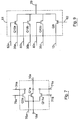
- the integrated circuit package 1 comprises two dies, namely, a first die 2 and a second die 3, both of which are mounted on a support, which in this case is a laminate 5, and the first and second dies 2 and 3 are encapsulated together with the laminate 5 in a resin encapsulating housing 6.
- the resin encapsulating housing 6 is represented by broken lines only.
- the laminate 5, which is effectively a miniature printed circuit board is also represented in broken lines only.
- Such laminates 5 in the form of miniature printed circuit boards will be well known to those skilled in the art.
- the first and second dies 2 and 3 could be mounted on any other suitable support instead of a laminate, for example, a lead frame.
- the first die 2 comprises a first integrated circuit, which in this embodiment of the invention is a digital signal processing circuit 8.
- the second die 3 comprises a second integrated circuit, which in this embodiment of the invention is an analogue integrated circuit, namely, a digital-to-analogue converting circuit 9.
- the digital signal processing circuit 8 and the digital-to-analogue converting circuit 9 are represented by broken lines on the first and second dies 2 and 3, respectively.
- the digital signal processing circuit 8 comprises a plurality of first input terminals 10 for receiving digital signals from an external source, however, for convenience only three of the first input terminals 10 are illustrated, and are indicated by the reference numerals 10a, 10b and 10c.
- a plurality of first output terminals 11 extend from the digital signal processing circuit 8 for outputting digital signals therefrom, however, for convenience only three of the first output terminals 11 are illustrated and are indicated by the reference numerals 11 a, 11 b and 11 c.
- a plurality of second input terminals 12 are provided to the digital-to-analogue converting circuit 9, the number of which corresponds to the number of first output terminals 11 from the digital signal processing circuit 8. However, for convenience only three second input terminals 12a, 12b and 12c are illustrated.
- a plurality of second output terminals 13 are provided from the digital-to-analogue converting circuit 9, however, for convenience in this case only three of the second output terminals 13a, 13b and 13c are illustrated.
- a switch circuit comprising a first integrated switch circuit 14 formed on the first die 2 and a second integrated switch circuit 15 formed on the second die 3, both of which will be described in detail below, is operable for selectively coupling the first input terminals 10 to corresponding externally accessible first external terminals 16, the first output terminals 11 to the corresponding second input terminals 12, and the second output terminals 13 to corresponding externally accessible second external terminals 17 for normal operation of the integrated circuit package 1.
- the first external terminals 16 are formed by hemispherical solder contacts on an exposed underside of the laminate 5 for receiving digital input signals
- the second external terminals 17 are also formed by hemispherical solder contacts on the exposed underside of the laminate 5 for outputting analogue output signals from the integrated circuit package 1 in response to the digital input signals applied to the first external terminals 16.
- first external terminals 16 are illustrated and indicated by the reference numerals 16a to 16c, in general, the number of first external terminals 16 will correspond to the number of first input terminals 10.
- second external terminals 17 have been illustrated and indicated by the reference numerals 17a, 17b and 17c, in general, the number of second external terminals 17 will correspond to the number of second output terminals 13.
- the digital-to-analogue converting circuit 9 may be provided with a single second output terminal 13 only, and thus, only a single second external terminal 17 would be provided, as in the embodiment of the invention which is described below with reference to Figs. 8 and 9 .
- the first and second external terminals 16 and 17 are suitable for coupling to corresponding terminals of tracks on a conventional printed circuit board for receiving digital signals from other digital devices on the printed circuit board or for delivering analogue signals to other devices on the printed circuit board.
- the first and second switch circuits 14 and 15 are also operable for facilitating selective testing of the digital signal processing circuit 8 and the digital-to-analogue converting circuit 9 between selectable combinations of the first input and output terminals 10 and 11 and selectable combinations of the second input and output terminals 12 and 13, so that a test signal applied to one of the first external terminals 16 is relayed to one of the corresponding first and second input terminals 10 and 12 of the selected one of the digital signal processing circuit 8 and the digital-to-analogue converting circuit 9 under test, and a response signal to the test signal on a selected one of the first and second output terminals 11 and 13 of the selected one of the digital signal processing circuit 8 and the digital-to-analogue converting circuit 9 under test is relayed to a corresponding one of the second external terminals 17.
- the operation of the first and second switch circuits 14 and 15 during testing of the digital signal processing circuit 8 and the digital-to-analogue converting circuit 9 is described in detail below.
- Each first input terminal 10 is coupled to a corresponding first input bond pad 18 on the first die 2 through a corresponding primary input switch 19 of the first switch circuit 14.
- the first input bond pads 18 and the primary input switches 19 corresponding to the first input terminals 10a, 10b and 10c are indicated by the reference numerals 18a, 18b and 18c, and 19a, 19b and 19c, respectively.
- Bond wires 20a, 20b and 20c couple the first input bond pads 18a, 18b and 18c to corresponding input tracks 21a, 21b and 21c on the laminate 5, which in turn terminate in the corresponding first external terminals 16a, 16b and 16c.
- the first output terminals 11 a, 11 b and 11c are coupled to corresponding first output bond pads 22a, 22b and 22c on the first die 2 through corresponding primary output switches 23a, 23b and 23c of the first switch circuit 14.
- Each second input terminal 12a, 12b and 12c is coupled to a corresponding second input bond pad 24a, 24b and 24c on the second die 3 through a corresponding secondary input switch 25a, 25b and 25c of the second switch circuit 15.
- Intermediate tracks 26 on the laminate 5 couple corresponding ones of the first output bond pads 22 and the second input bond pads 24 through corresponding bond wires 27 and 28.
- the intermediate tracks 26 and the bond wires 27 and 28 corresponding to the first output bond pads 22a, 22b and 22c, and the second input bond pads 24a, 24b and 24c, respectively, are indicated by the reference numerals 26a, 26b and 26c, and 27a, 27b and 27c, and 28a, 28b and 28c, respectively.
- first output bond pads 22 and the second input bond pads 24 could be coupled directly to each other by corresponding bond wires, thus avoiding the need for the intermediate tracks 26, and indeed, if the dies were stacked one above the other on the laminate 5, instead of being placed side by side on the laminate 5, the first output bond pads 22 and the second input bond pads 24 would normally be coupled directly to each other by corresponding bond wires.
- Each second output terminal 13 is coupled to a corresponding second output bond pad 29 on the second die 3 through a corresponding secondary output switch 30 of the second switch circuit 15.
- the second output bond pads 29 and the secondary output switches 30 corresponding to the second output terminals 13a, 13b and 13c, respectively, are indicated by the reference numerals 29a, 29b and 29c, and 30a, 30b and 30c, respectively.
- Bond wires 31 a, 31 b and 31 c couple the second output bond pads 29a, 29b and 29c to corresponding output tracks 32a, 32b and 32c on the laminate 5 which terminate in the second external terminals 17a, 17b and 17c.
- the first input bond pads 18 would be coupled by bond wires to corresponding fingers of the lead frame, which would terminate in externally accessible pin connectors, which in turn would project through the encapsulating housing 6.
- the second output bond pads 29 would be coupled by bond wires to other corresponding fingers of the lead frame, which would likewise terminate in externally accessible pin connectors extending through the encapsulating housing 6.
- First electrically conductive tracks 34a, 34b and 34c on the first die 2 couple the corresponding ones of the primary input and output switches 19a, 19b and 19c and 23a, 23b and 23c, respectively.
- Second electrically conductive tracks 35a, 35b and 35c formed on the second die 3 couple the corresponding ones of the secondary input and output switches 25a, 25b and 25c and 30a, 30b and 30c, respectively.
- the corresponding pair of the primary input and output switches 19a and 23a co-operate with the first electrically conductive track 34a for selectively coupling the first external terminal 16a to one of the first input terminal 10a, the first output terminal 11a and the first output bond pad 22a.
- the corresponding pairs of the primary input and output switches 19b and 23b, and 19c and 23c co-operate with the first electrically conductive tracks 34b and 34c, respectively, for selectively coupling the first external terminals 16b and 16c to one of the corresponding first input terminal 10b, 10c, the corresponding first output terminal 11 b, 11 c and the corresponding first output bond pad 22b, 22c, respectively.
- the corresponding pair of the secondary input and output switches 25a and 30a co-operate with the second electrically conductive track 35a for selectively coupling the second external terminal 17a to one of the second output terminals 13a, the second input terminal 12a and the second input bond pad 24a.
- the corresponding pairs of secondary input and output switches 25b and 30b, and 25c and 30c co-operate with the second electrically conductive tracks 35b and 35c, respectively, for selectively coupling the second external terminals 17b and 17c to one of the corresponding second output terminals 13b, 13c, the corresponding second input terminal 12b, 12c, and the corresponding second input bond pads 24b and 24c, respectively.
- a control circuit comprising a first control circuit provided by a first integrated JTAG circuit 38 and a second control circuit provided by a second integrated JTAG circuit 39 controls operation of the first and second switch circuits 14 and 15, respectively.
- the first JTAG circuit 38 is fabricated on the first die 2 for controlling the operation of the primary input and output switches 19 and 23.
- the second JTAG circuit 39 is fabricated on the second die 3 for controlling the operation of the secondary input switches 25 and the secondary output switches 30.
- First and second serial data ports 40 and 41 to the first and second JTAG circuits 38 and 39, respectively, are coupled by bond wires (not shown) to first and second control tracks 43 and 44, respectively, of the corresponding laminates 5.
- the first and second control tracks 43 and 44 terminate in externally accessible first and second external control terminals 45 and 46, respectively, for applying logic control signals to the first and second JTAG circuits 38 and 39 for in turn controlling the operation of primary input and output switches 19 and 23 and the secondary input and output switches 25 and 30, respectively.
- the switch contacts a and b of the primary input switches 19, the primary output switches 23, the secondary input switches 25 and the secondary output switches 30 are switched to the contacts zero of the respective switches 19, 23, 25 and 30.
- the first external terminals 16 are coupled to the corresponding first input terminals 10
- the first output terminals 11 are coupled to the corresponding second input terminals 12
- the second output terminals 13 are coupled to the corresponding second external terminals 17.
- the switch contact a of the primary input switch 19a is switched to the contact zero.
- the switch contacts a and b of the primary output switch 23a are also both switched to contact zero.
- the switch contact a of the secondary input switch 25a is switched to the contact one, and the switch contact b of the secondary input switch 25a is switched to the contact zero.
- the switch contact a of the secondary output switch 30 is coupled to the contact one.
- the first external terminal 16a is coupled directly to the first input terminal 10a of the digital signal processing circuit 8, and the first output terminal 11 a of the digital signal processing circuit 8 is coupled directly to the second external terminal 17a through the second electrically conductive track 35a.
- the second input terminal 12a and the second output terminal 13a of the digital-to-analogue converting circuit 9 are disconnected from the second input and output bond pads 24a and 29a, respectively, and in other words, are effectively floating.
- the switch contact a of the primary input switch 19a is switched to the contact one.
- the switch contact a of the primary output switch 23a is switched to contact zero; and the switch contact b of the primary output switch 23a is switched to the contact one.
- the two switch contacts a and b of the secondary input switch 25a are both switched to corresponding contacts zero, and the switch contact a of the secondary output switch 30a is switched to the contact zero.
- the first external terminal 16a is coupled directly to the second input terminal 12a of the digital-to-analogue converting circuit 9 through the first electrically conductive track 34a, and the second output terminal 13a is coupled directly to the second external terminal 17a.
- an appropriate test signal is applied to the first external terminal 16a and a response signal is read on the second external terminal 17a.
- the primary input and output switches 19a and 23c are configured for coupling the first external terminal 16a to the first input terminal 10a, and for coupling the first output terminal 11 c to the first output bond pad 22c.
- the secondary input and output switches 25c and 30c are configured for coupling the second input bond pad 24c directly to the second output bond pad 29c through the second electrically conductive track 35c. Accordingly, by applying an appropriate test signal to the first external terminal 16a, a response signal can be read on the second external terminal 17c for testing the function of the digital signal processing circuit 8 between the first input terminal 10a and the first output terminal 11 c.
- the primary input switch 19a comprises a first primary input transistor Q1a, and a second primary input transistor Q2a, both of which are fabricated as CMOS devices on the first die 2.
- the first primary input transistor Q1a couples the first input bond pad 18a to the corresponding first input terminal 10a.
- the second primary input transistor Q2a couples the first input bond pad 18a to the first electrically conductive track 34a.
- a logic control signal applied on a first primary control line 50a by the first JTAG circuit 38 controls the operation of the first and second primary input transistors Q1a and Q2a for configuring the primary input switch 19a appropriately.
- the logic signal on the corresponding control line 50a is applied directly to the first primary input transistor Q1a, and is applied to the second primary input transistor Q2a through an inverter 52a, so that when the first primary input transistor Q1a is operating in the low impedance state, the second primary input transistor Q2a is operating in the high impedance state and vice versa.
- the primary input switches 19b and 19c are similar to the primary input switch 19a, and further description should not be required.
- Logic control signals applied on first primary control lines 50b and 50c control the operation of corresponding first and second primary input transistors of the primary input switches 19b and 19c.
- the primary output switch 23a comprises three transistors, namely, a first primary output transistor Q3a, and second and third primary output transistors Q4a and Q5a, respectively.
- the first, second and third primary output transistors Q3a, Q4a and Q5a are fabricated as CMOS devices on the first die 2.
- the first primary output transistor Q3a couples the first output terminal 11 a to the first output bond pad 22a.
- the second primary output transistor Q4a couples the first output terminal 11a to the first electrically conductive track 34a, while the third primary output transistor Q5a couples the first output bond pad 22a to the first electrically conductive track 34a.
- Control logic signals applied on second, third and fourth primary control lines 54a, 55a and 56a by the first JTAG circuit 38 control the operation of the first, second and third primary output transistors Q3a, Q4a and Q5a, respectively for appropriately configuring the primary output switch 23a.
- the primary output switches 23b and 23c are similar to the primary output switch 23a, and corresponding second, third and fourth primary control lines 54b and 54c, 55b and 55c, and 56b and 56c are provided from the first JTAG circuit 38 for operating the first, second and third primary output transistors of the primary output switches 23b and 23c, respectively.
- the secondary input switch 25a comprises first, second and third secondary input transistors Q6a, Q7a and Q8a, all of which are fabricated as CMOS devices on the second die 3.
- the first secondary input transistor Q6a couples the second input bond pad 24a with the corresponding second input terminal 12a.
- the second secondary input transistor Q7a couples the second input terminal 12a with the corresponding second electrically conductive track 35a
- the third secondary input transistor Q8a couples the second input bond pad 24a with the corresponding second electrically conductive track 35a.
- the first, second and third secondary input transistors Q6a, Q7a and Q8a are operated under the control of the second JTAG circuit 39 by logic control signals applied to first, second and third secondary control lines 58a, 59a and 60a, respectively, for appropriately configuring the secondary input switch 25a.
- the secondary input switches 25b and 25c are similar to the secondary input switch 25a, the first, second and third secondary input transistors of the secondary input switches 25b and 25c are similarly controlled by logic control signals applied by the second JTAG circuit 39 on corresponding first, second and third secondary control lines 58b, 58c, 59b, 59c and 60b and 60c, respectively.
- the secondary output switch 30a comprises a first secondary output transistor Q9a which couples the second output bond pad 29a with the second output terminal 13a and a second secondary output transistor Q10a which couples the second output bond pad 29a with the corresponding second electrically conductive track 35a.
- the first and second secondary output transistors Q9a and Q10a are fabricated as CMOS devices on the second die 3.
- the first and second secondary output transistors Q9a and Q10a are operated under the control of the second JTAG circuit 39 by logic signals applied on a fourth secondary control line 62a.
- An inverter 64a inverts the logic signal to the second secondary output transistor Q10 so that when the first secondary output transistor Q9a is operating in the low impedance state the second secondary output transistor Q10a is operating in the high impedance state and vice versa.
- the secondary output switches 30b and 30c are similar to the secondary output switch 30a, and control logic signals on corresponding fourth secondary control lines 62b and 62c from the second JTAG circuit 39 control the operation of the first and second secondary output transistors of the secondary output switches 30b and 30c, respectively.
- the primary input and output switches 19 and 23 and the secondary input and output switches 25 and 30 are appropriately configured to carry out each test to which the digital signal processing circuit 8 and the digital-to-analogue converting circuit 9 are to be subjected, by inputting appropriate signals to the first and second JTAG circuits 38 and 39 through the first and second external control terminals 45 and 46, respectively.
- an appropriate test signal is applied to one or more of the first external terminals 16, and one or more corresponding response signals are read on the appropriate one or more second external terminals 17.
- first and second JTAG circuits 38 and 39 for setting the primary input and output switches 19 and 23 and the secondary input and output switches 25 and 30 for normal operation, with the first primary input transistors Q1, the first primary output transistors Q3, the first secondary input transistors Q6 and the first secondary output transistors Q9 in the low impedance state, and the second primary input transistors Q2, the second and third primary output transistors Q4 and Q5, the second and third secondary input transistors Q7 and Q8 and the second secondary output transistor Q10 all in the high impedance state.
- FIG. 6 there is illustrated an integrated circuit package according to another embodiment of the invention, indicated generally by the reference numeral 70.
- the integrated circuit package 70 is substantially similar to the integrated circuit package 1 described with reference to Figs. 1 to 5 , and similar components are identified by the same reference numerals.
- the main difference between the integrated circuit package 70 and the integrated circuit package 1 is that in this embodiment of the invention the first external terminal 16a is a general purpose I/O terminal, and all tests on the integrated circuit package 70 are carried out by applying appropriate test signals to the I/O terminal 16a.
- the primary input switches 19 are three-way switches, and the switch contact a of the respective primary input switches 19 may be selectively coupled to the contacts zero, one or two.
- the contact two of each primary input switch 19 is coupled to the switch contact of the next adjacent primary input switch 19 through a corresponding intermediate electrically conductive track 71.
- the primary input switch 19a is coupled to the primary input switch 19b by the intermediate electrically conductive track 71 a
- the primary input switch 19b is coupled to the primary input switch 19c by the intermediate electrically conductive track 71b, and so on.
- the switch contact a of the primary input switch 19a is switched to the contact zero which in turn is coupled to the first input terminal 10a.
- the switch contact a of the primary input switch 19a is switched to the contact one which is coupled to the corresponding first electrically conductive track 34a.
- the primary output switch 23a and the secondary input switch 25a and the appropriate secondary output switch 30 are then appropriately configured as described with reference to the integrated circuit package 1.
- the switch contact a of the primary input switch 19a is switched to the contact two which is coupled to the intermediate electrically conductive track 71 a. Thereafter the primary input switches 19b and 19c are set, depending on whether the test signal applied to the I/O terminal 16a is to be applied to the first input terminal 10b or 10c. If the test signal is to be applied to the first input terminal 10b, the switch contact a of the primary input switch 19b is switched to the contact zero.
- the switch contact a of the primary input switch 19b is switched to the contact two, and the switch contact a of the primary input switch 19c is switched to the contact zero.
- the primary output switches 23 and the secondary input and output switches 25 and 30 are then appropriately configured.
- the first primary input switch 19a of the integrated circuit package 70 is illustrated, and comprises three transistors, namely, a first primary input transistor Q1a, a second primary input transistor Q2a and a third primary input transistor Q11a, all of which are fabricated as CMOS devices on the first die 2.
- the first primary input transistor Q1a is similar to the first primary input transistor Q1a of the integrated circuit package 1 and couples the first input bond pad 18a with the first input terminal 10a of the digital signal processing circuit 8.
- the second primary input transistor Q2a is similar to the second primary input transistor Q2a of the integrated circuit package 1, and couples the first input bond pad 18a with the corresponding first electrically conductive track 34a.
- the third primary input transistor Q11a couples the first input bond pad 18a with the intermediate electrically conductive track 71 a for selectively coupling the first input bond pad 18a with the first input bond pad 18b corresponding to the first external terminal 16b.
- the first, second and third primary input transistors Q1a, Q2a and Q11 a are individually controlled by logic signals applied on a first primary control line 75a and first and second intermediate control lines 76a and 77a, respectively, by the first JTAG circuit 38.
- the first primary input switches 19b and 19c are similar to the first primary input switch 19a, and each comprises a first, second and a third primary input transistor, which are respectively controlled by logic control signals on first control lines 75b and 75c and on first and second intermediate control lines 76b and 76c, and 77b and 77c, respectively, by the first JTAG circuit 38.
- the integrated circuit package 70 of Figs. 6 and 7 is similar to the integrated circuit package 1 described with reference to Figs. 1 to 5 , and its operation is likewise similar, with the exception that all test signals are applied to the I/O terminal 16a.
- the first primary input transistors Q1 of the primary input switches 19 are operated under the control of the first JTAG circuit 38 in the low impedance state, while the second and third primary input transistors Q2 and Q11 of the primary input switches 19 are operated in the high impedance state under the control of the first JTAG circuit 38.
- the transistors of the primary output switches 23 and the secondary input switches 25 and the secondary output switches 30 are operated as already described with reference to the integrated circuit package 1 described with reference to Figs. 1 to 5 .
- FIG. 8 and 9 there is illustrated an integrated circuit package according to the invention, indicated generally by the reference numeral 80, according to another embodiment of the invention.
- the integrated circuit package 80 is substantially similar to the integrated circuit package 1, and similar components are identified by the same reference numerals.
- the main difference between the integrated circuit package 80 and the integrated circuit package 1 is that in the integrated circuit package 80 only one second external terminal 17 is provided on which an analogue output signal corresponding to a digital input signal applied to the first external terminals 16 is outputted. Additionally, only one single second output terminal 13 is provided from the digital-to-analogue converting circuit 9 of the second die 3.
- a single second output bond pad 29 is provided on the second die 3, and is coupled by a bond wire 31 to an output track 32 of the laminate 5, which terminates in the single second external terminal 17.
- only one secondary output switch 81 is provided for selectively coupling the second output bond pad 29 to the second output terminal 13 of the digital-to-analogue converting circuit 9 for normal operation of the integrated circuit package 80, and to a selected one of the second electrically conductive tracks 35a, 35b and 35c for facilitating testing of the integrated circuit package 80.
- the secondary output switch 81 comprises a first secondary output transistor Q9 which couples the second output bond pad 29 to the second output terminal 13.
- the first secondary output transistor Q9 of the secondary output switch 81 of the integrated circuit package 80 is similar to the first secondary output transistor Q9 of the secondary output switches 30 of the integrated circuit package 1 described with reference to Figs. 1 to 5 .
- a plurality of second secondary output transistors Q10a to Q10c are provided for coupling the second output bond pad 29 to the respective second electrically conductive tracks 35a to 35c. Needless to say, it will be appreciated that the number of second secondary output transistors Q10 will depend on the number of second electrically conductive tracks 35.
- One second secondary output transistor Q10 will be provided for each second electrically conductive track 35.
- the first and second secondary output transistors Q9 and Q10 of the secondary output switches 30 of the integrated circuit package 1 are fabricated as CMOS devices on the second die 3.
- the first secondary output transistor Q9 is operated under the control of the second JTAG circuit 39 by a logic signal which is applied on a fourth secondary control line 62.
- Each of the second secondary output transistors Q10a to Q10c are operated under the control of the second JTAG circuit 39 by logic signals applied on corresponding fifth secondary control lines 82a to 82c.
- the logic control signals are applied on the fourth secondary control line 62 and the fifth secondary control lines 82 so that when one of the first and second secondary output transistors Q9 and Q10 is operated in the low impedance state, the remaining ones of the first and second secondary output transistors Q9 and Q10 are operated in the high impedance state, so that the second output bond pad 29 is only connected to one of the second output terminal 13 and the second electrically conductive tracks 35 at one time, and is isolated from the remaining ones of the second output terminal 13 and the second electrically conductive tracks 35.
- operation of the integrated circuit package 80 is substantially similar to the operation of the integrated circuit package 1.
- the primary input and output switches 19 and 23 and the secondary input switches 25 are operated as already described.
- the secondary output switch 81 is operated with the second output bond pad 29 coupled to the second output terminal 13 of the digital-to-analogue converting circuit 9, and isolated from the second electrically conductive tracks 35.
- the primary input and output switches 19 and 23 and the secondary input switches 25 are appropriately operated for testing the function in the selected one of the digital signal processing circuit 8 and the digital-to-analogue converting circuit 9 as already described.
- the secondary output switch 81 is operated for coupling the second output bond pad 29 to the second output terminal 13 of the digital-to-analogue converting circuit 9, and with the primary input and output switches 19 and 23 and the secondary input switches 25 appropriately operated, a test signal is applied to the appropriate one of the first external terminals 16, and an analogue output signal is read from the second external terminal 17.
- the secondary output switch 81 is operated for coupling the second output bond pad 29 to the appropriate one of the second electrically conductive tracks 35, and the primary input and output switches 19 and 23 and the secondary input switches 25 are appropriately operated as already described with reference to the integrated circuit package 1.
- the integrated circuit package 80 and its operation is similar to that of the integrated circuit package 1.
- FIG. 10 there is illustrated an integrated circuit package according to another embodiment of the invention, indicated generally by the reference numeral 85.
- the integrated circuit package 85 is substantially similar to the integrated circuit package 1 described with reference to Figs. 1 to 5 and similar components are identified by the same reference numerals.
- the main difference between the integrated circuit package 85 and the integrated circuit package 1 is that the integrated circuit package 85 comprises three dies, namely, the first die 2, the second die 3, and an intermediate die 86 comprising an integrated circuit 87, which is coupled between the digital signal processing circuit 8 and the digital-to-analogue converting circuit 9 by the switch circuit.
- the switch circuit as well as comprising the first and second integrated switch circuits 14 and 15 on the first and second dies 2 and 3, also comprises an intermediate integrated switch circuit 88, which is formed on the intermediate die 86.
- the first and second dies 2 and 3 are identical to the first and second dies 2 and 3 of the integrated circuit package 1, and the digital signal processing circuit 8 of the first die 2 comprises a plurality of first input terminals 10 and first output terminals 11, although only one first input terminal 10 and one first output terminal 11 is illustrated.
- Each first input terminal 10 of the digital signal processing circuit 8 is coupled to a corresponding first input bond pad 18 through a corresponding primary input switch 19, which in turn is connected to a corresponding first external terminal 16 through a corresponding bond wire 20 and a corresponding track 21 of the laminate 5.
- each first output terminal 11 to the corresponding first output bond pad 22 through the corresponding primary output switch 23 is similar to that of the coupling of each first output terminal 11 to the corresponding first output bond pad 22 of the first die 2 of the integrated circuit package 1, as is the coupling of the corresponding primary input and output switches 19 and 23 through the first electrically conductive tracks 34 on the first die 2.
- each second input terminal 12 to the digital-to-analogue converting circuit 9 of the second die 3 to the corresponding second input bond pad 24 through the corresponding secondary input switch 25 is similar to the coupling of the second input terminals 12 to the second input bond pads 24 of the second die 3 of the integrated circuit package 1, as is the coupling of each second output terminal 13 of the digital-to-analogue converting circuit 9 to the corresponding second output bond pad 31 through the corresponding secondary output switch 30.
- the coupling of the corresponding secondary input and output switches 25 and 30 through the corresponding second electrically conductive tracks 35 is similar to that of the integrated circuit package 1.
- the integrated circuit 87 of the intermediate die 86 may be any type of integrated circuit, for example, a digital or an analogue integrated circuit. However, typically, the integrated circuit 87 of the intermediate die 86 would be a digital signal processing circuit or possibly a memory circuit.
- a plurality of input terminals 89, only one of which is illustrated, are provided to the integrated circuit 87, and a plurality of output terminals 90, only one of which is illustrated, are provided from the integrated circuit 87. Each input terminal 89 is selectively coupled to a corresponding input bond pad 91 by a corresponding intermediate input switch 92 of the intermediate switch circuit 88.
- Each intermediate input switch 92 is similar to the secondary input switches 25 of the second die 2 and comprises transistors similar to the transistors Q6, Q7 and Q8 of Fig. 4 , which are fabricated on the intermediate die 86.
- Each output terminal 90 of the integrated circuit 87 is selectively coupled to a corresponding output bond pad 93 by a corresponding intermediate output switch 94 of the intermediate switch circuit 88.
- Each intermediate output switch 94 is similar to the primary output switches 23 of the first die 2 and comprises transistors which are similar to the transistors Q3, Q4 and Q5 as illustrated in Fig. 3 , and which are fabricated on the intermediate die 86.
- Each intermediate input switch 92 is coupled to a corresponding one of the intermediate output switches 94 by an intermediate electrically conductive track 95.
- the intermediate electrically conductive tracks 95 are similar to the first and second electrically conductive tracks 34 and 35.
- the first and second dies 2 and 3 and the intermediate die 86 are mounted on a laminate 96, which is substantially similar to the laminate 5 of the integrated circuit package 1, and are effectively coupled in series.
- Each input bond pad 91 is coupled to a corresponding first output bond pad 22 of the first die 2 by a corresponding bond wire 97
- each output bond pad 93 is coupled to a corresponding one of the second input bond pads 24 of the second die 3 by a corresponding bond wire 98.
- each input bond pad 91 of the intermediate die 86 could be coupled to the first output bond pad 22 of the first die 2 through a corresponding track of the laminate 96, and similarly, each output bond pad 93 of the intermediate die 86 could be coupled to the second input bond pad 24 of the second die 3 through a corresponding track of the laminate 96, in a similar manner as the first output bond pads 22 are coupled to the corresponding second input bond pads 24 of the integrated circuit package 1.
- the first and second dies 2 and 3 and the intermediate die 86 are encapsulated together on and with the laminate 96 in a resin encapsulating housing 99.
- the first and second external terminals 16 and 17 are similarly formed by hemispherical solder contacts on an exposed under surface of the laminate 96, as in the case of the integrated circuit package 1.
- a control circuit is provided on the intermediate die 87 and is provided by a JTAG circuit, similar to the JTAG circuits 38 and 39 of the first and second dies 2 and 3 for controlling the operation of the transistors of the intermediate input and output switches 92 and 94 for in turn operating the intermediate input and output switches 92 and 94.
- the primary input and output switches 19 and 23 and the secondary input and output switches 25 and 30 are operated as already described with reference to the integrated circuit package 1 for normal operation of the integrated circuit package 85. Additionally, in normal operation of the integrated circuit package 85, the intermediate input and output switches 92 and 94 are operated so that each input terminal 89 of the integrated circuit 87 is coupled to the corresponding input bond pad 91, and each output terminal 90 of the integrated circuit 87 is coupled to the corresponding output bond pad 93.
- Testing of functions of the digital signal processing circuit 8 and the digital-to-analogue converting circuit 9 between selected pairs of first input and output terminals 10 and 11 and second input and output terminals 12 and 13 is similar to that already described with reference to the integrated circuit package 1, with the addition that the appropriate intermediate input switch 92 and the appropriate intermediate output switch 94 are operated for coupling the appropriate one of the first output bond pads 22 to the appropriate one of the second input bond pads 24 through the appropriate intermediate electrically conductive track 95.
- the intermediate input switch 92 corresponding to the selected input terminal 89 is operated for coupling the selected input terminal 89 to the corresponding input bond pad 91
- the intermediate output switch 94 corresponding to the selected output terminal 90 is operated for coupling the selected output terminal 90 to the corresponding output bond pad 93.
- the appropriate ones of the primary input and output switches 19 and 23 are operated for coupling the appropriate first external terminal 16 directly to the input bond pad 91 corresponding to the selected input terminal 89 through the corresponding first electrically conductive track 34.
- the appropriate ones of the secondary input and output switches 25 and 30 are operated for coupling the output bond pad 93 corresponding to the selected output terminal 90 directly to the appropriate one of the second external terminals 17 through the corresponding second electrically conductive track 35.
- a suitable test signal is then applied to the appropriate first external terminal 16, and a response signal is read from the appropriate second external terminal 17.
- the integrated circuit package 85 is similar to the integrated circuit package 1 and its operation is otherwise similar.
- the integrated circuit package 85 has been described as comprising one intermediate die which is effectively connected in series between the first and second dies 2 and 3, it is envisaged that a plurality of intermediate dies may be provided, and where a plurality of intermediate dies are provided between the first and second dies, the integrated circuits of the respective intermediate dies may be coupled in series between the first and second integrated circuits of the first and second dies, or may be coupled in parallel with each other between the first and second integrated circuits of the first and second dies, or some of the integrated circuits of the intermediate dies may be coupled in series, while others would be coupled in parallel with each other.
- each first external terminal 16 is adapted for receiving a test signal
- the first external terminal 16a has been described as being suitable for applying test signals to the integrated circuit package
- the first input terminals of the digital signal processing circuit 8 may be grouped in groups of first input terminals, and a corresponding first external terminal would be provided for each first input terminal, and in such a case only one of the first external terminals 16 of each group would be adapted for applying test signals to the respective groups of first input terminals to the digital signal processing circuit 8.
- first and second control circuits have been described as being JTAG circuits, any other suitable control circuits may be provided for controlling operation of the primary input and output switches and the secondary input and output switches of the first and second dies and the intermediate input and output switches of the intermediate dies.
- first and second switch circuits and intermediate switch circuit may be provided for facilitating selectively applying test signals to the first input and output terminals of the digital signal processing circuit and the second input and output terminals and of the digital-to-analogue converting circuit, and to the input and output terminals of the integrated circuits of the intermediate dies.
- the integrated circuit packages have been described with the first and second dies, and the intermediate die or dies, as the case may be, lying side by side on the laminate, it is envisaged in many cases that the dies will be stacked one above the other on the laminate. It is also envisaged that instead of mounting the dies on a laminate, the dies may be mounted on a lead frame, or any other suitable support.
- all the dies of the integrated circuit packages may comprise digital signal processing circuits, or alternatively, all the dies may comprise analogue signal processing circuits, and in other embodiments of the invention it is envisaged that the first die may comprise an analogue signal processing circuit, and the second die may comprise a digital signal processing circuit. Indeed, where the first die comprises an analogue circuit it is envisaged that only one external terminal may be provided for the analogue circuit.
- first and second integrated circuits on the first and second dies of the integrated circuit packages have been described as being a digital signal processing circuit, and a digital-to-analogue converting circuit, respectively, any other integrated circuits could be provided on the first and second dies.
- the first and second integrated circuits have been described as being a digital signal processing circuit and a digital-to-analogue converting circuit, solely for the purpose of illustration.
Landscapes
- Physics & Mathematics (AREA)
- Engineering & Computer Science (AREA)
- Computer Hardware Design (AREA)
- Computing Systems (AREA)
- General Engineering & Computer Science (AREA)
- Mathematical Physics (AREA)
- Semiconductor Integrated Circuits (AREA)
- Tests Of Electronic Circuits (AREA)
Claims (13)
- Integrierter Schaltungsbaustein (1), der Folgendes umfasst:einen ersten Chip (2) mit einer ersten integrierten Schaltung (8) darauf und mindestens einer ersten Eingangsklemme (10a) und mehreren ersten Ausgangsklemmen (11a) der ersten integrierten Schaltung (8),einen zweiten Chip (3) mit einer zweiten integrierten Schaltung (9) darauf und mehreren zweiten Eingangsklemmen (12a) und einer zweiten Ausgangsklemme (13a) der zweiten integrierten Schaltung (9),eine erste externe Klemme (16a), die von außerhalb des integrierten Schaltungsbausteins (1) zugänglich ist,eine zweite externe Klemme (17a), die von außerhalb des integrierten Schaltungsbausteins (1) zugänglich ist, undeinen Schalterstromkreis (14, 15) mit mindestens einem primären Eingangsschalter (19), der zum gezielten Verbinden der ersten Eingangsklemme (10a) mit der ersten externen Klemme (16a) dient, einem sekundären Ausgangsschalter (30), der zum gezielten Verbinden der zweiten Ausgangsklemmen (13a, 13b, 13c) mit der zweiten externen Klemme (17a) dient, mehreren primären Ausgangsschaltern (23) und mehreren sekundären Eingangsschaltern (25), wobei die primären Ausgangsschalter und die sekundären Eingangsschalter zum gezielten Verbinden der zweiten Eingangsklemmen (12a, 12b, 12c) mit entsprechenden ersten Ausgangsklemmen (11a, 12b, 12c) dienen, wobei bei normalem Betrieb des integrierten Schaltungsbausteins die erste Eingangsklemme (10a) mit der ersten externen Klemme (16a), die zweite Ausgangsklemme (13a) mit der zweiten externen Klemme (17a) und jede zweite Eingangsklemme (12a) mit einer entsprechenden ersten Ausgangsklemme (11a) verbunden ist, so dass der erste und der zweite Chip (2, 3) Teil eines gemeinsamen Signalpfades bilden, wobei der Schalterstromkreis (14, 15) einen ersten und einen zweiten Schalterstromkreis umfasst, wobei der erste Schalterstromkreis als erster integrierter Schalterstromkreis auf dem ersten Chip implementiert ist und den primären Eingangsschalter und die primären Ausgangsschalter umfasst und der zweite Schalterstromkreis als zweiter integrierter Schalterstromkreis auf dem zweiten Chip implementiert ist und die sekundären Eingangsschalter und den sekundären Ausgangsschalter umfasst, und der erste Chip eine erste elektrische Leiterbahn (35) zum gezielten Verbinden des primären Eingangsschalters (19) und eines primären Ausgangsschalters (23) und der zweite Chip eine zweite elektrische Leiterbahn zum gezielten Verbinden eines sekundären Eingangsschalters (25) und des sekundären Ausgangsschalters (30) umfasst,wobei der Schalterstromkreis (14, 15) gezielt zum Ermöglichen des Prüfens der ersten integrierten Schaltung (8) dient, so dass ein an der ersten externen Klemme (16a) anliegendes Prüfsignal über den primären Eingangsschalter (19) zur ersten Eingangsklemme (10a) und ein Antwortsignal auf das Prüfsignal an einer ersten Ausgangsklemme über den primären Ausgangsschalter (23), den sekundären Eingangsschalter (25), die zweite elektrische Leiterbahn und den sekundären Ausgangsschalter direkt zur zweiten externen Klemme (17a) weitergeleitet wird, undwobei der Schalterstromkreis (14, 15) gezielt zum Ermöglichen des Prüfens der zweiten integrierten Schaltung (9) dient, so dass ein an der ersten externen Klemme (16a) anliegendes Prüfsignal über den primären Eingangsschalter (19), die erste elektrische Leiterbahn, den primären Ausgangsschalter (23) und den sekundären Eingangsschalter (25) direkt zu einer zweiten Eingangsklemme (12a) und ein Antwortsignal auf das Prüfsignal an der zweiten Ausgangsklemme (13a) über den sekundären Ausgangsschalter (30) zur zweiten externen Klemme (17a) weitergeleitet wird,wobei der Schalterstromkreis gezielt dazu dient, ein gezieltes Prüfen der ersten und der zweiten integrierten Schaltung zwischen von dem Schalterstromkreis wählbaren Kombinationen der ersten Eingangsklemme und der ersten Ausgangsklemmen und zwischen von dem Schalterstromkreis wählbaren Kombinationen der zweiten Eingangsklemmen und der zweiten Ausgangsklemme zu ermöglichen, so dass ein an der ersten externen Klemme anliegendes Prüfsignal zu einer ausgewählten unter den ersten und den zweiten Eingangsklemmen der ausgewählten unter der ersten und der zweiten integrierten Schaltung und ein Antwortsignal auf das Prüfsignal an einer ausgewählten unter den ersten und den zweiten Ausgangsklemmen einer ausgewählten unter den ersten und den zweiten Ausgangsklemmen der ausgewählten unter der ersten und der zweiten integrierten Schaltung zu den zweiten externen Klemmen weitergeleitet wird.
- Integrierter Schaltungsbaustein nach Anspruch 1, bei dem der Schalterstromkreis zum gezielten Verbindena) der ersten externen Klemme mit einer der ersten Ausgangsklemmen und/oderb) zum gezielten Verbinden der zweiten externen Klemme mit einer der zweiten Eingangsklemmen dient.
- Integrierter Schaltungsbaustein nach Anspruch 1 oder 2, bei dem der Schalterstromkreis zum gezielten Verbinden der zweiten Eingangsklemmen mit jeweils entsprechenden ersten Ausgangsklemmen für einen normalen Betrieb des integrierten Schaltungsbausteins dient.
- Integrierter Schaltungsbaustein nach Anspruch 3, bei dem der Schalterstromkreis:a) zum gezielten Verbinden der ersten externen Klemme mit einer ausgewählten unter auswählbaren von zumindest einigen der zweiten Eingangsklemmen,b) zum gezielten Verbinden der ersten externen Klemme mit einer ausgewählten unter auswählbaren von zumindest einigen der ersten Ausgangsklemmen oder/undc) zum gezielten Verbinden der zweiten externen Klemme mit einer ausgewählten unter auswählbaren von zumindest einigen der ersten Ausgangsklemmen dient.
- Integrierter Schaltungsbaustein nach einem der vorhergehenden Ansprüche, bei dem mehrere erste Eingangsklemmen für die erste integrierte Schaltung bereitgestellt sind und der Schalterstromkreis zum gezielten Verbinden der ersten externen Klemme mit einer ausgewählten unter auswählbaren von zumindest einigen der ersten Eingangsklemmen dient.
- Integrierter Schaltungsbaustein nach Anspruch 5, bei dem mehrere von außen zugängliche erste externe Klemmen bereitgestellt sind, wobei zumindest einige der ersten externen Klemmen jeweiligen ersten Eingangsklemmen entsprechen, und der Schalterstromkreis zum gezielten Verbinden der ersten externen Klemmen mit den entsprechenden ersten Eingangsklemmen für den normalen Betrieb des integrierten Schaltungsbausteins dient, und bei dem wahlweise mindestens eine der ersten externen Klemmen mehreren der ersten Eingangsklemmen entspricht und der Schalterstromkreis zum gezielten Verbinden einer ausgewählten unter auswählbaren der mehreren ersten Eingangsklemmen, die der mindestens einen der ersten externen Klemmen entspricht, mit der entsprechenden ersten externen Klemme dient.
- Integrierter Schaltungsbaustein nach einem der vorhergehenden Ansprüche, bei dem mehrere zweite Ausgangsklemmen (13a, 13b, 13c) für die zweite integrierte Schaltung (3) bereitgestellt sind und der Schalterstromkreis zum gezielten Verbinden der zweiten externen Klemme mit einer ausgewählten unter auswählbaren der zweiten Ausgangsklemmen dient.
- Integrierter Schaltungsbaustein nach Anspruch 7, bei dem mehrere von außen zugängliche zweite externe Klemmen bereitgestellt sind, wobei zumindest einige der zweiten externen Klemmen jeweiligen der zweiten Ausgangsklemmen entsprechen, und der Schalterstromkreis zum gezielten Verbinden der zweiten externen Klemmen mit den entsprechenden zweiten Ausgangsklemmen für einen normalen Betrieb des integrierten Schaltungsbausteins dient.
- Integrierter Schaltungsbaustein nach einem der vorhergehenden Ansprüche, bei dem mindestens ein Zwischenchip (88) bereitgestellt ist, auf dem sich eine integrierte Schaltung und eine Eingangsklemme und eine Ausgangsklemme der integrierten Schaltung befindet, wobei der Schalterstromkreis zum gezielten Verbinden einer der zweiten Eingangsklemmen der zweiten integrierten Schaltung des zweiten Chips mit einer der ersten Ausgangsklemmen der ersten integrierten Schaltung des ersten Chips über die integrierte Schaltung des mindestens einen Zwischenchips für einen normalen Betrieb des integrierten Schaltungsbausteins und zum Ermöglichen eines gezielten Prüfens der integrierten Schaltung des Zwischenchips dient, so dass ein an der ersten externen Klemme anliegendes Prüfsignal zur Eingangsklemme der integrierten Schaltung des Zwischenchips und ein Antwortsignal auf das Prüfsignal an der Ausgangsklemme der integrierten Schaltung des Zwischenchips zur zweiten externen Klemme weitergeleitet wird.
- Integrierter Schaltungsbaustein nach Anspruch 9, bei dem mehrere Zwischenchips bereitgestellt sind, auf denen sich jeweils eine integrierte Schaltung und eine Eingangsklemme und eine Ausgangsklemme der integrierten Schaltung befindet, wobei der Schalterstromkreis zum gezielten Verbinden einer der zweiten Eingangsklemmen der zweiten integrierten Schaltung des zweiten Chips mit einer der ersten Ausgangsklemmen der ersten integrierten Schaltung des ersten Chips über die integrierten Schaltungen zumindest einiger der Zwischenchips für einen normalen Betrieb des integrierten Schaltungsbausteins und zum gezielten Prüfen der integrierten Schaltung eines ausgewählten der Zwischenchips dient, so dass ein an der ersten externen Klemme anliegendes Prüfsignal zur Eingangsklemme der integrierten Schaltung des ausgewählten Zwischenchips und ein Antwortsignal auf das Prüfsignal an der Ausgangsklemme der integrierten Schaltung des ausgewählten Zwischenchips zur zweiten externen Klemme weitergeleitet wird.
- Integrierter Schaltungsbaustein nach einem der vorhergehenden Ansprüche, bei dem ein erstes Eingangs-Bondpad, das jeder ersten externen Klemme entspricht, an dem ersten Chip bereitgestellt ist, wobei jedes erste Eingangs-Bondpad mit der entsprechenden ersten externen Klemme verbunden ist, und sich über den Schalterstromkreis gezielt mit einer ausgewählten unter auswählbaren der entsprechenden einen oder mehreren der ersten Eingangsklemmen, der entsprechenden einen oder mehreren der ersten Ausgangsklemmen und der entsprechenden einen oder mehreren der zweiten Eingangsklemmen verbinden lässt,
ein erstes Ausgangs-Bondpad, das jeder ersten Ausgangsklemme entspricht, an dem ersten Chip bereitgestellt ist, wobei sich jedes erste Ausgangs-Bondpad über den Schalterstromkreis gezielt mit einem unter der entsprechenden ersten Ausgangsklemme und dem entsprechenden ersten Eingangs-Bondpad ausgewählten Element verbinden lässt,
ein zweites Eingangs-Bondpad, das jeder zweiten Eingangsklemme entspricht, an dem zweiten Chip bereitgestellt ist, wobei jedes zweite Eingangs-Bondpad mit dem entsprechenden ersten Ausgangs-Bondpad verbunden ist und sich über den Schalterstromkreis gezielt mit einem unter der entsprechenden zweiten Eingangsklemme und der zweiten externen Klemme ausgewählten Element verbinden lässt, und
ein zweites Ausgangs-Bondpad, das jeder zweiten externen Klemme entspricht, an dem zweiten Chip bereitgestellt ist, wobei jedes zweite Ausgangs-Bondpad mit der entsprechenden zweiten externen Klemme verbunden ist und sich über den Schalterstromkreis gezielt mit einem unter der entsprechenden zweiten Ausgangsklemme und dem zweiten Eingangs-Bondpad ausgewählten Element verbinden lässt. - Integrierter Schaltungsbaustein nach Anspruch 1, bei dem mindestens ein Zwischenchip bereitgestellt ist, auf dem sich eine integrierte Schaltung und mehrere Eingangsklemmen und mindestens eine Ausgangsklemme der integrierten Schaltung befinden, wobei der Schalterstromkreis zum gezielten Verbinden der zweiten Eingangsklemme der zweiten integrierten Schaltung des zweiten Chips mit der ersten Ausgangsklemme der ersten integrierten Schaltung des ersten Chips über die integrierte Schaltung des mindestens einen Zwischenchips für einen normalen Betrieb des integrierten Schaltungsbausteins und zum Ermöglichen eines gezielten Prüfens der integrierten Schaltung eines des mindestens einen Zwischenchips zwischen auswählbaren Kombinationen der Eingangs- und der Ausgangsklemmen der integrierten Schaltung des ausgewählten unter dem mindestens einen Zwischenchip dient, so dass ein an einer oder einer der ersten externen Klemmen anliegendes Prüfsignal zu einer ausgewählten der Eingangsklemmen der integrierten Schaltung des ausgewählten Zwischenchips und ein Antwortsignal auf das Prüfsignal an der Ausgangsklemme oder der ausgewählten Ausgangsklemme der integrierten Schaltung des ausgewählten Zwischenchips zu der zweiten externen Klemme weitergeleitet wird.
- Verfahren zum Herstellen eines integrierten Schaltungsbausteins mit zwei Chips mit jeweiligen darauf ausgebildeten integrierten Schaltungen, wobei Eingangs- und Ausgangsklemmen der integrierten Schaltungen zum Ermöglichen des Prüfens der integrierten Schaltungen direkt adressierbar sind, wobei das Verfahren Folgendes umfasst:Bereitstellen eines ersten der beiden Chips, wobei sich auf dem ersten Chip eine integrierte Schaltung mit einer ersten Eingangsklemme und mehreren ersten Ausgangsklemmen der ersten integrierten Schaltung befindet,Bereitstellen eines zweiten der beiden Chips, wobei sich auf dem zweiten Chip eine zweite integrierte Schaltung mit mehreren zweiten Eingangsklemmen und einer zweiten Ausgangsklemme der zweiten integrierten Schaltung befindet,Bereitstellen einer ersten externen Klemme, die von außerhalb des integrierten Schaltungsbausteins zugänglich ist,Bereitstellen einer zweiten externen Klemme, die von außerhalb des integrierten Schaltungsbausteins zugänglich ist, undBereitstellen eines Schalterstromkreises mit einem primären Eingangsschalter, der zum gezielten Verbinden der ersten Eingangsklemme mit der ersten externen Klemme dient, einem sekundären Ausgangsschalter, der zum gezielten Verbinden der zweiten Ausgangsklemme mit der zweiten externen Klemme dient, mehreren primären Ausgangsschaltern (23) und mehreren sekundären Eingangsschaltern (25), wobei die primären Ausgangsschalter und die sekundären Eingangsschalter zum gezielten Verbinden der zweiten Eingangsklemmen (12a) mit den entsprechenden ersten Ausgangsklemmen (11a) dienen, wobei bei normalem Betrieb des integrierten Schaltungsbausteins die erste Eingangsklemme (10a) mit der ersten externen Klemme (16a), die zweite Ausgangsklemme (13a) mit der zweiten externen Klemme (17a) und jede zweite Eingangsklemme (12a) mit einer entsprechenden ersten Ausgangsklemme (11a) verbunden ist, so dass der erste und der zweite Chip (2, 3) Teil eines gemeinsamen Signalpfades bilden, wobei der Schalterstromkreis dazu dient, ein gezieltes Prüfen der ersten und der zweiten integrierten Schaltung zu ermöglichen,wobei der Schalterstromkreis einen ersten und einen zweiten Schalterstromkreis umfasst, wobei der erste Schalterstromkreis als erster integrierter Schalterstromkreis auf dem ersten Chip implementiert ist und den primären Eingangsschalter und die primären Ausgangsschalter umfasst und der zweite Schalterstromkreis als zweiter integrierter Schalterstromkreis auf dem zweiten Chip implementiert ist und die sekundären Eingangsschalter und den sekundären Ausgangsschalter umfasst und der erste Chip eine erste elektrische Leiterbahn (35) zum gezielten Verbinden des primären Eingangsschalters (19) und des primären Ausgangsschalters (23) und der zweite Chip eine zweite elektrische Leiterbahn zum gezielten Verbinden des sekundären Eingangsschalters (25) und des sekundären Ausgangsschalters (30) umfasst,wobei beim Prüfen der ersten integrierten Schaltung ein an der ersten externen Klemme anliegendes Prüfsignal über den primären Eingangsschalter der ersten integrierten Schaltung zur ersten Eingangsklemme und ein Antwortsignal auf das Prüfsignal von einer ersten Ausgangsklemme der ersten integrierten Schaltung über den primären Ausgangsschalter (23), den sekundären Eingangsschalter (25) und den sekundären Ausgangsschalter direkt zur zweiten externen Klemme weitergeleitet wird undwobei beim Prüfen der zweiten integrierten Schaltung ein an der ersten externen Klemme anliegendes Prüfsignal über den primären Eingangsschalter (19), primären Ausgangsschalter (23) und den sekundären Eingangsschalter (25) zu einer zweiten Eingangsklemme der zweiten integrierten Schaltung und ein Antwortsignal auf das Prüfsignal von der zweiten Ausgangsklemme der zweiten integrierten Schaltung über den sekundären Ausgangsschalter (30) zur zweiten externen Klemme weitergeleitet wird,wobei der Schalterstromkreis gezielt dazu dient, ein gezieltes Prüfen der ersten und der zweiten integrierten Schaltung zwischen von dem Schalterstromkreis wählbaren Kombinationen der ersten Eingangsklemme und der ersten Ausgangsklemmen und zwischen von dem Schalterstromkreis wählbaren Kombinationen der zweiten Eingangsklemmen und der zweiten Ausgangsklemme zu ermöglichen, so dass ein an der ersten externen Klemme anliegendes Prüfsignal zu einer ausgewählten unter den ersten und den zweiten Eingangsklemmen der ausgewählten unter der ersten und der zweiten integrierten Schaltung und ein Antwortsignal auf das Prüfsignal an einer ausgewählten unter den ersten und den zweiten Ausgangsklemmen einer ausgewählten unter den ersten und den zweiten Ausgangsklemmen der ausgewählten unter der ersten und der zweiten integrierten Schaltung zu der zweiten externen Klemme weitergeleitet wird.
Applications Claiming Priority (2)
| Application Number | Priority Date | Filing Date | Title |
|---|---|---|---|
| US11/344,372 US7579689B2 (en) | 2006-01-31 | 2006-01-31 | Integrated circuit package, and a method for producing an integrated circuit package having two dies with input and output terminals of integrated circuits of the dies directly addressable for testing of the package |
| PCT/IE2007/000003 WO2007088526A1 (en) | 2006-01-31 | 2007-01-22 | An integrated circuit package, and a method for producing an integrated circuit package having two dies with input and output terminals of integrated circuits of the dies directly addressable for testing of the package |
Publications (3)
| Publication Number | Publication Date |
|---|---|
| EP1979757A1 EP1979757A1 (de) | 2008-10-15 |
| EP1979757B1 true EP1979757B1 (de) | 2017-05-17 |
| EP1979757B8 EP1979757B8 (de) | 2017-07-12 |
Family
ID=38321435
Family Applications (1)
| Application Number | Title | Priority Date | Filing Date |
|---|---|---|---|
| EP07700693.0A Ceased EP1979757B8 (de) | 2006-01-31 | 2007-01-22 | Integriertes schaltungspaket und verfahren zur herstellung eines integrierten schaltungspakets mit zwei matrizen mit eingangs- und ausgangsklemmen für integrierte schaltungen der matrizen zum testen des pakets |
Country Status (4)
| Country | Link |
|---|---|
| US (1) | US7579689B2 (de) |
| EP (1) | EP1979757B8 (de) |
| CN (1) | CN101379407B (de) |
| WO (1) | WO2007088526A1 (de) |
Families Citing this family (8)
| Publication number | Priority date | Publication date | Assignee | Title |
|---|---|---|---|---|
| JP2008203089A (ja) * | 2007-02-20 | 2008-09-04 | Ricoh Co Ltd | マルチチップ半導体装置およびその検査方法ならびに該マルチチップ半導体装置を組み込んだ電子機器 |
| US9772460B2 (en) * | 2010-02-23 | 2017-09-26 | Luxtera, Inc. | Method and system for implementing high-speed interfaces between semiconductor dies in optical communication systems |
| US8762586B2 (en) * | 2012-06-30 | 2014-06-24 | Silicon Laboratories Inc. | Apparatus for mixed signal interface acquisition circuitry and associated methods |
| US9083323B2 (en) * | 2013-02-11 | 2015-07-14 | Qualcomm Incorporated | Integrated circuit identification and dependability verification using ring oscillator based physical unclonable function and age detection circuitry |
| US9304163B2 (en) * | 2013-11-07 | 2016-04-05 | Qualcomm Incorporated | Methodology for testing integrated circuits |
| WO2017113294A1 (en) * | 2015-12-31 | 2017-07-06 | Texas Instruments Incorporated | Multi-channel mcm with test circuitry for inter-die bond wire checking |
| JP6655461B2 (ja) * | 2016-04-28 | 2020-02-26 | ラピスセミコンダクタ株式会社 | 半導体装置、半導体チップ及び半導体チップのテスト方法 |
| CN109964277B (zh) * | 2016-10-20 | 2023-08-11 | 德州仪器公司 | 用于检测及移除有缺陷集成电路封装的方法及设备 |
Citations (3)
| Publication number | Priority date | Publication date | Assignee | Title |
|---|---|---|---|---|
| JPH0191547A (ja) * | 1987-06-09 | 1989-04-11 | Fujitsu Ltd | 共通バスシステム |
| US20030079166A1 (en) * | 2001-09-20 | 2003-04-24 | Vermeulen Hubertus Gerardus Hendrikus | Electronic device |
| GB2403299A (en) * | 2003-06-25 | 2004-12-29 | Hewlett Packard Development Co | Bypassing a device in a scan chain |
Family Cites Families (9)
| Publication number | Priority date | Publication date | Assignee | Title |
|---|---|---|---|---|
| US4703436A (en) * | 1984-02-01 | 1987-10-27 | Inova Microelectronics Corporation | Wafer level integration technique |
| US5969538A (en) * | 1996-10-31 | 1999-10-19 | Texas Instruments Incorporated | Semiconductor wafer with interconnect between dies for testing and a process of testing |
| US6721913B1 (en) * | 2000-04-24 | 2004-04-13 | Marvell International, Ltd. | Method and apparatus for testing an interface between separate hardware components |
| US6970362B1 (en) * | 2000-07-31 | 2005-11-29 | Intel Corporation | Electronic assemblies and systems comprising interposer with embedded capacitors |
| JP3839267B2 (ja) * | 2001-03-08 | 2006-11-01 | 株式会社ルネサステクノロジ | 半導体装置及びそれを用いた通信端末装置 |
| DE10123758B4 (de) * | 2001-05-16 | 2008-04-03 | Texas Instruments Deutschland Gmbh | Multi-Chip-Modul mit mehreren integrierten Halbleiterschaltungen |
| US6825683B1 (en) * | 2002-04-18 | 2004-11-30 | Cypress Semiconductor Corporation | System and method for testing multiple integrated circuits that are in the same package |
| JP2004317382A (ja) * | 2003-04-18 | 2004-11-11 | Sony Corp | 半導体装置 |
| JP2005283432A (ja) * | 2004-03-30 | 2005-10-13 | Denso Corp | 半導体ウエハおよびその半導体ウエハを用いた半導体装置の製造方法 |
-
2006
- 2006-01-31 US US11/344,372 patent/US7579689B2/en active Active
-
2007
- 2007-01-22 CN CN2007800040844A patent/CN101379407B/zh not_active Expired - Fee Related
- 2007-01-22 EP EP07700693.0A patent/EP1979757B8/de not_active Ceased
- 2007-01-22 WO PCT/IE2007/000003 patent/WO2007088526A1/en not_active Ceased
Patent Citations (3)
| Publication number | Priority date | Publication date | Assignee | Title |
|---|---|---|---|---|
| JPH0191547A (ja) * | 1987-06-09 | 1989-04-11 | Fujitsu Ltd | 共通バスシステム |
| US20030079166A1 (en) * | 2001-09-20 | 2003-04-24 | Vermeulen Hubertus Gerardus Hendrikus | Electronic device |
| GB2403299A (en) * | 2003-06-25 | 2004-12-29 | Hewlett Packard Development Co | Bypassing a device in a scan chain |
Also Published As
| Publication number | Publication date |
|---|---|
| CN101379407A (zh) | 2009-03-04 |
| WO2007088526A1 (en) | 2007-08-09 |
| EP1979757A1 (de) | 2008-10-15 |
| EP1979757B8 (de) | 2017-07-12 |
| CN101379407B (zh) | 2011-04-20 |
| US20070176632A1 (en) | 2007-08-02 |
| US7579689B2 (en) | 2009-08-25 |
Similar Documents
| Publication | Publication Date | Title |
|---|---|---|
| EP1979757B1 (de) | Integriertes schaltungspaket und verfahren zur herstellung eines integrierten schaltungspakets mit zwei matrizen mit eingangs- und ausgangsklemmen für integrierte schaltungen der matrizen zum testen des pakets | |
| US6897554B2 (en) | Test circuit and multi-chip package type semiconductor device having the test circuit | |
| KR0163756B1 (ko) | 전자 모듈 소켓장치 | |
| EP0174224B1 (de) | Integrierte Schaltung vom Chip-auf-Chip-Typ | |
| US5581176A (en) | Analog autonomous test bus framework for testing integrated circuits on a printed circuit board | |
| US6009259A (en) | Emulation System | |
| KR100317761B1 (ko) | 반도체 장치 | |
| US20040041580A1 (en) | Multichip module and testing method thereof | |
| EP0414014B1 (de) | Halbleiteranordnung und Verfahren zum Test derselben | |
| US6714002B2 (en) | Integrated semiconductor circuit and multi-chip module with a plurality of integrated semiconductor circuits | |
| US5463560A (en) | Semiconductor integrated circuit device | |
| US7176560B2 (en) | Semiconductor device having a chip—chip structure | |
| JPH11111913A (ja) | 機能変更可能な半導体装置 | |
| KR100221415B1 (ko) | 신호처리장치 | |
| JPH0513662A (ja) | マルチチツプモジユール | |
| US6936911B1 (en) | Semiconductor integrated circuit device | |
| US5140189A (en) | WSI decoder and patch circuit | |
| US7865787B2 (en) | Testing embedded circuits with the aid of a separate supply voltage | |
| CN118539907B (zh) | 一种射频开关用控制芯片、射频开关模块及其封装流程 | |
| JP4457648B2 (ja) | 半導体装置 | |
| JP2004037254A (ja) | スキャンテスト装置 | |
| US6765302B2 (en) | Semiconductor module having a configurable data width of an output bus, and a housing configuration having a semiconductor module | |
| JP2005228932A (ja) | 半導体装置 | |
| JPH02105452A (ja) | 半導体集積回路の出力回路 | |
| US6448849B1 (en) | Semiconductor devices including a switch mounted thereon and a module loaded with the same |
Legal Events
| Date | Code | Title | Description |
|---|---|---|---|
| PUAI | Public reference made under article 153(3) epc to a published international application that has entered the european phase |
Free format text: ORIGINAL CODE: 0009012 |
|
| 17P | Request for examination filed |
Effective date: 20080605 |
|
| AK | Designated contracting states |
Kind code of ref document: A1 Designated state(s): DE FR GB |
|
| DAX | Request for extension of the european patent (deleted) | ||
| RBV | Designated contracting states (corrected) |
Designated state(s): DE FR GB |
|
| RAP1 | Party data changed (applicant data changed or rights of an application transferred) |
Owner name: MEDIATEK INC. |
|
| 17Q | First examination report despatched |
Effective date: 20120228 |
|
| REG | Reference to a national code |
Ref country code: DE Ref legal event code: R079 Ref document number: 602007051019 Country of ref document: DE Free format text: PREVIOUS MAIN CLASS: G01R0031317000 Ipc: H03K0019173000 |
|
| GRAP | Despatch of communication of intention to grant a patent |
Free format text: ORIGINAL CODE: EPIDOSNIGR1 |
|
| RIC1 | Information provided on ipc code assigned before grant |
Ipc: H03K 19/173 20060101AFI20161208BHEP Ipc: G01R 31/28 20060101ALI20161208BHEP Ipc: G01R 31/3167 20060101ALI20161208BHEP |
|
| INTG | Intention to grant announced |
Effective date: 20161219 |
|
| GRAS | Grant fee paid |
Free format text: ORIGINAL CODE: EPIDOSNIGR3 |
|
| GRAA | (expected) grant |
Free format text: ORIGINAL CODE: 0009210 |
|
| AK | Designated contracting states |
Kind code of ref document: B1 Designated state(s): DE FR GB |
|
| RAP1 | Party data changed (applicant data changed or rights of an application transferred) |
Owner name: MEDIATEK INC. |
|
| REG | Reference to a national code |
Ref country code: GB Ref legal event code: FG4D |
|
| RAP2 | Party data changed (patent owner data changed or rights of a patent transferred) |
Owner name: MEDIATEK INC. |
|
| REG | Reference to a national code |
Ref country code: DE Ref legal event code: R096 Ref document number: 602007051019 Country of ref document: DE |
|
| REG | Reference to a national code |
Ref country code: FR Ref legal event code: PLFP Year of fee payment: 12 |
|
| REG | Reference to a national code |
Ref country code: DE Ref legal event code: R097 Ref document number: 602007051019 Country of ref document: DE |
|
| PLBE | No opposition filed within time limit |
Free format text: ORIGINAL CODE: 0009261 |
|
| STAA | Information on the status of an ep patent application or granted ep patent |
Free format text: STATUS: NO OPPOSITION FILED WITHIN TIME LIMIT |
|
| 26N | No opposition filed |
Effective date: 20180220 |
|
| P01 | Opt-out of the competence of the unified patent court (upc) registered |
Effective date: 20230607 |
|
| PGFP | Annual fee paid to national office [announced via postgrant information from national office to epo] |
Ref country code: DE Payment date: 20240129 Year of fee payment: 18 Ref country code: GB Payment date: 20240129 Year of fee payment: 18 |
|
| PGFP | Annual fee paid to national office [announced via postgrant information from national office to epo] |
Ref country code: FR Payment date: 20240125 Year of fee payment: 18 |
|
| REG | Reference to a national code |
Ref country code: DE Ref legal event code: R119 Ref document number: 602007051019 Country of ref document: DE |
|
| GBPC | Gb: european patent ceased through non-payment of renewal fee |
Effective date: 20250122 |
|
| PG25 | Lapsed in a contracting state [announced via postgrant information from national office to epo] |
Ref country code: DE Free format text: LAPSE BECAUSE OF NON-PAYMENT OF DUE FEES Effective date: 20250801 |
|
| PG25 | Lapsed in a contracting state [announced via postgrant information from national office to epo] |
Ref country code: GB Free format text: LAPSE BECAUSE OF NON-PAYMENT OF DUE FEES Effective date: 20250122 |
|
| PG25 | Lapsed in a contracting state [announced via postgrant information from national office to epo] |
Ref country code: FR Free format text: LAPSE BECAUSE OF NON-PAYMENT OF DUE FEES Effective date: 20250131 |