EP1978347A2 - Verfahren und Vorrichtung zum Testen der Lötbarkeit von elektrischen Bauteilen - Google Patents
Verfahren und Vorrichtung zum Testen der Lötbarkeit von elektrischen Bauteilen Download PDFInfo
- Publication number
- EP1978347A2 EP1978347A2 EP08161255A EP08161255A EP1978347A2 EP 1978347 A2 EP1978347 A2 EP 1978347A2 EP 08161255 A EP08161255 A EP 08161255A EP 08161255 A EP08161255 A EP 08161255A EP 1978347 A2 EP1978347 A2 EP 1978347A2
- Authority
- EP
- European Patent Office
- Prior art keywords
- solder
- electrical component
- contact portion
- load sensor
- vacuum chamber
- Prior art date
- Legal status (The legal status is an assumption and is not a legal conclusion. Google has not performed a legal analysis and makes no representation as to the accuracy of the status listed.)
- Granted
Links
Images

Classifications
-
- B—PERFORMING OPERATIONS; TRANSPORTING
- B23—MACHINE TOOLS; METAL-WORKING NOT OTHERWISE PROVIDED FOR
- B23K—SOLDERING OR UNSOLDERING; WELDING; CLADDING OR PLATING BY SOLDERING OR WELDING; CUTTING BY APPLYING HEAT LOCALLY, e.g. FLAME CUTTING; WORKING BY LASER BEAM
- B23K31/00—Processes relevant to this subclass, specially adapted for particular articles or purposes, but not covered by only one of the preceding main groups
- B23K31/12—Processes relevant to this subclass, specially adapted for particular articles or purposes, but not covered by only one of the preceding main groups relating to investigating the properties, e.g. the weldability, of materials
-
- G—PHYSICS
- G01—MEASURING; TESTING
- G01N—INVESTIGATING OR ANALYSING MATERIALS BY DETERMINING THEIR CHEMICAL OR PHYSICAL PROPERTIES
- G01N13/00—Investigating surface or boundary effects, e.g. wetting power; Investigating diffusion effects; Analysing materials by determining surface, boundary, or diffusion effects
- G01N13/02—Investigating surface tension of liquids
-
- B—PERFORMING OPERATIONS; TRANSPORTING
- B23—MACHINE TOOLS; METAL-WORKING NOT OTHERWISE PROVIDED FOR
- B23K—SOLDERING OR UNSOLDERING; WELDING; CLADDING OR PLATING BY SOLDERING OR WELDING; CUTTING BY APPLYING HEAT LOCALLY, e.g. FLAME CUTTING; WORKING BY LASER BEAM
- B23K2101/00—Articles made by soldering, welding or cutting
- B23K2101/36—Electric or electronic devices
- B23K2101/40—Semiconductor devices
Definitions
- SMT surface mount technology
- Current instruments being used for solderability testing essentially include analytical balances with a built-in clock poised over molten solder.
- the SMT component is suspended from the bottom of the balance prior to testing.
- the SMT component has flux applied to it and is dipped into the molten solder.
- the solder may be in a bath or formed as a small globule.
- the resulting surface tension of the molten solder wetting to the component is measured by the analytical balance over a period of time.
- the resulting measurements are used to plot a graph of the wetting force (i.e. the surface tension) versus time, which is then used to determine whether the component has suitable wetting properties for providing good solderability.
- the sample component In order for the quality of solderability of the component to be considered adequate, the sample component must wet quickly enough during the time that it is in contact with the molten solder and must exhibit a wetting force large enough to provide a suitably sized solder fillet in the completed solder joint.
- the limitations of the testing arrangements described above make it difficult to accurately measure the wetting forces of the newest small components. This is in part because of the smaller amounts of solder required for the smaller pins.
- the sensitivity of the equipment used to measure the wetting forces in such arrangements is inadequate for the smaller wetting forces required to be measured for the smaller SMT pin sizes.
- Some such arrangements have a smallest full scale division of force measurement in milliNewtons, which is inadequate to measure forces in the order of microNewtons.
- the newly developed small pin sizes and smaller solder amounts required for such pin sizes means that greater precision in force measurement is needed.
- thermal currents in air at standard pressure may be high enough relative to the small wetting forces that unreliable results would be recorded or the test may be compromised.
- Embodiments described herein relate generally to methods and system for use in determining solderability of an electrical component.
- a system for measuring solderability of an electrical component comprising: a vacuum chamber; a load sensor having a contact portion, the contact portion being disposed within the vacuum chamber; a first receptacle for containing solder; a platform or support disposed within the vacuum chamber in relation to the contact portion and having a component mounting surface for mounting the electrical component; and a control and communications module for causing relative movement between the platform or support and the load sensor so that a contact surface of the electrical component is brought into close proximity with the contact portion, whereby, when the contact portion has solder thereon and the solder is brought into contact with the contact surface, the load sensor measures force arising from wetting of the solder to the contact surface; wherein the control and communications module is configured to monitor sensed conditions within the system.
- the force occurring under contact may change over time, depending on the degree of solderability of the electrical component.
- Providing a vacuum chamber in which the solderability testing can be carried out may allow for minimization of thermal currents that might cause spurious results in the surface tension measurements.
- a load sensor having a measurement accuracy similar to that of an atomic force microscope may be used. Such precision allows measurement of forces in the order of microNewtons.
- the system preferably has the first receptacle positioned on the platform.
- a first heating element is associated with the first receptacle for heating the solder in the first receptacle.
- a first temperature sensor is also provided for sensing a temperature of the solder in the first receptacle.
- the system further preferably comprises a second receptacle containing flux, the second receptacle being positioned on the platform.
- the first and second receptacles have, in one embodiment, closable openings arranged to be closed when the contact portion is not being dipped into the respective first or second receptacle.
- a second heating element is disposed on the platform.
- the second heating element has an upper surface comprising the component mounting surface.
- the mounting member is disposed on or adjacent the component mounting surface.
- a second temperature sensor is provided for sensing a temperature of the second heating element.
- the load sensor preferably comprises a projection and the contact portion is disposed at a tip of the projection.
- the load sensor further comprises a third heating element disposed adjacent the contact portion.
- a cooling element may also be disposed around the projection distally of the contact portion.
- the projection comprises a downwardly pending pin of relatively small diameter, for example in the order of 0.5 mm or less.
- the platform is disposed below the contact portion of the projection.
- the contact portion is formed of a material that is electrically and thermally minimally - or non-conductive.
- the system preferably comprises a computer processor and a memory storing computer program instructions which, when executed by the computer processor, cause the computer processor to control operation of the load sensor and the control and communications module.
- the system preferably comprises a user interface to allow configuration of the solderability testing and initiation of a testing procedure.
- the system may also comprise an imaging device such as a camera.
- the output of the imaging device may be provided to at least one of: a display independent of the computer system; and a display of the computer system.
- control and communications module may be configured to monitor at least one of: an internal pressure of the vacuum chamber; a platform position; and/or a sensed temperature.
- control and communications module may be configured to monitor images received from the imaging device.
- the at least one electrical component is preferably disposed below the contact portion.
- the step of causing relative movement comprises moving the at least one electrical component relative to the contact surface while the contact surface is held stationary.
- the step of applying flux comprises moving a flux container containing flux relative to the contact portion to dip the contact portion into the flux container.
- the step of applying solder comprises moving a solder container containing solder relative to the contact portion to dip the contact portion into the solder container.
- the flux container and the solder container each is mounted to a moveable platform within the vacuum chamber or a member supported by the platform.
- Images may be captured during testing using an imaging device.
- the method may further comprise verifying that an appropriate amount of solder is suspended from tip portion of load sensor once tip portion has been dipped in solder container, using the imaging device.
- Yet another aspect may comprise apparatus for use in determining solderability of an electrical component, comprising: a vacuum chamber; a load sensor having a contact portion, the contact portion being disposed within the vacuum chamber; a platform or support disposed within the vacuum chamber in relation to the contact portion and having a component mounting surface for mounting the electrical component; and a control module for causing relative movement between the platform or support and the load sensor so that a contact surface of the electrical component is brought into close proximity with the contact portion, whereby, when the contact portion has solder thereon and the solder is brought into contact with the contact surface, the load sensor measures force arising from wetting of the solder to the contact surface.
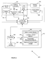
- FIG. 1 there is shown a schematic front view of an example testing apparatus 100 for testing the solderability of electrical components 140, such as SMT components, by measuring wetting forces (i.e. surface tension) during contact of solder to the electrical components 140.
- the schematic of the apparatus shown in Figure 1 is not to scale and is provided for purposes of illustration only.
- the testing apparatus 100 has a vacuum chamber 110 with a load sensor 120 mounted thereon and a support module platform 130 contained within the vacuum chamber 110.
- One or more electrical components 140 are mounted to, or otherwise held on, a heating element 144 that is situated on the platform 130.
- a flux receptacle such as flux container 150
- a solder receptacle such as solder container 152.
- the vacuum chamber 110 also has an imaging device 170, such as a camera, directed to capture images during testing. The images can be viewed by the test supervisor to make positioning adjustments during testing, if necessary.
- a temperature sensor 162 is positioned to take temperature measurements corresponding to the temperature of the solder in solder container 152.
- the temperature can be measured using a thermal camera.
- solder container 152 has a closeable opening at its top which is biased towards a closed position but which is openable for dipping tip portion 128 into the solder.
- the closeable opening of solder container 152 is preferably opened automatically by a form of mechanical actuation when tip portion 128 is positioned above solder container 152 and approaches within a predetermined vertical distance of the opening.
- Pin 124 may have a cooling coil 126 disposed along a portion of pin 124 proximally of contact tip portion 128.
- Pin 124 preferably also has a third heating element 180 for resistive heating of tip portion 128. Because tip portion 128 needs to be heated to a relatively high temperature by heating element 180, cooling element 126 is used to reduce heat conduction to the measurement and control portion 125 of load sensor 120.
- User interface 220 may include any suitable interface means, such as a display, keyboard and mouse.
- One or more of the software modules stored in memory 240 may include existing software applications, for example such as those which may be provided with the purchase of elements in apparatus 100.
- load sensor 120 may have appropriate software that is commercially available with purchase of load sensor 120 and which may constitute the load measurement module 244.
- platform control module 242 may comprise software provided by the maker of platform 130 and specifically tailored for control of platform 130.
- Other of the software modules stored in memory 240 may include routines developed in an appropriate commercially available software application for control and measurement purposes, such as LabVIEW TM available from National Instruments.
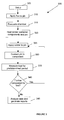
- solder container 152 is heated by heating element 154 to ensure that the solder therein is in a molten state. If necessary, wiper 156 is used to wipe the dross from the top of the molten solder once it has melted. While the solder is melted, heating elements 144 and 180 are used to heat the electrical components 140 and tip portion 128, respectively.
- solder to tip portion 128 is done by moving platform 130 so as to position solder container 152 beneath tip portion 128 and then raising platform 130 so as to immerse tip portion 128 in solder container 152 by about 2.5 mm. During or prior to solder container 152 being raised towards tip portion 128, its top opening is opened and, once tip portion 128 is withdrawn, the opening is again closed. Once solder has been applied to the tip portion 128 and platform 130 has been lowered to withdraw tip portion 128 from solder container 152, camera 170 may be used to visually verify that an appropriate amount of solder is suspended from tip portion 128. Signals from load sensor 120 may also be used to verify that an appropriate amount of solder is suspended from tip portion 128.
- test surface of an electrical component includes conductive pads and other forms of electrical terminations or leads.
- SMT components as one form of electrical component, it should be understood that other kinds of electrical components that rely on solder to form electrical connections on current boards may be the subject of testing using the described embodiments.
Landscapes
- Engineering & Computer Science (AREA)
- Mechanical Engineering (AREA)
- Physics & Mathematics (AREA)
- Health & Medical Sciences (AREA)
- Life Sciences & Earth Sciences (AREA)
- Chemical & Material Sciences (AREA)
- Analytical Chemistry (AREA)
- Biochemistry (AREA)
- General Health & Medical Sciences (AREA)
- General Physics & Mathematics (AREA)
- Immunology (AREA)
- Pathology (AREA)
- Electric Connection Of Electric Components To Printed Circuits (AREA)
- Investigating Or Analyzing Materials Using Thermal Means (AREA)
- Investigating Or Analyzing Materials By The Use Of Electric Means (AREA)
Applications Claiming Priority (1)
| Application Number | Priority Date | Filing Date | Title |
|---|---|---|---|
| EP06112413A EP1845360B1 (de) | 2006-04-10 | 2006-04-10 | Vorrichtung und Verfahren zur Lötbarkeitsmessung von elektrischen Bauelementen |
Related Parent Applications (2)
| Application Number | Title | Priority Date | Filing Date |
|---|---|---|---|
| EP06112413A Division EP1845360B1 (de) | 2006-04-10 | 2006-04-10 | Vorrichtung und Verfahren zur Lötbarkeitsmessung von elektrischen Bauelementen |
| EP06112413.7 Division | 2006-04-10 |
Publications (3)
| Publication Number | Publication Date |
|---|---|
| EP1978347A2 true EP1978347A2 (de) | 2008-10-08 |
| EP1978347A3 EP1978347A3 (de) | 2008-12-17 |
| EP1978347B1 EP1978347B1 (de) | 2011-08-17 |
Family
ID=37075534
Family Applications (2)
| Application Number | Title | Priority Date | Filing Date |
|---|---|---|---|
| EP08161255A Active EP1978347B1 (de) | 2006-04-10 | 2006-04-10 | Verfahren und Vorrichtung zum Testen der Lötbarkeit von elektrischen Bauteilen |
| EP06112413A Active EP1845360B1 (de) | 2006-04-10 | 2006-04-10 | Vorrichtung und Verfahren zur Lötbarkeitsmessung von elektrischen Bauelementen |
Family Applications After (1)
| Application Number | Title | Priority Date | Filing Date |
|---|---|---|---|
| EP06112413A Active EP1845360B1 (de) | 2006-04-10 | 2006-04-10 | Vorrichtung und Verfahren zur Lötbarkeitsmessung von elektrischen Bauelementen |
Country Status (4)
| Country | Link |
|---|---|
| EP (2) | EP1978347B1 (de) |
| AT (2) | ATE520971T1 (de) |
| CA (1) | CA2583853C (de) |
| DE (1) | DE602006003067D1 (de) |
Families Citing this family (3)
| Publication number | Priority date | Publication date | Assignee | Title |
|---|---|---|---|---|
| US8910775B2 (en) * | 2012-08-10 | 2014-12-16 | Asm Technology Singapore Pte Ltd | Transfer apparatus for transferring electronic devices |
| CN113776992B (zh) * | 2021-08-27 | 2024-02-23 | 河北光兴半导体技术有限公司 | 测试熔体表面张力的方法 |
| CN114682948B (zh) * | 2022-03-04 | 2023-10-31 | 广东风华高新科技股份有限公司 | 片式元器件的可焊性测试方法、装置及系统 |
Citations (4)
| Publication number | Priority date | Publication date | Assignee | Title |
|---|---|---|---|---|
| JPH0572153A (ja) | 1991-09-11 | 1993-03-23 | Sony Corp | クリームはんだのはんだ付け性測定装置 |
| JPH0772064A (ja) | 1993-06-24 | 1995-03-17 | Sony Corp | 電子部品のハンダ付け性試験方法及び装置 |
| US6286368B1 (en) | 2000-09-18 | 2001-09-11 | General Electric Company | Self-immersing wetting balance |
| EP1236991A1 (de) | 2001-02-27 | 2002-09-04 | Sony Corporation | Vorrichtung und Verfahren zur Lötbarkeitmessung |
Family Cites Families (3)
| Publication number | Priority date | Publication date | Assignee | Title |
|---|---|---|---|---|
| JPS6247292A (ja) | 1985-08-26 | 1987-02-28 | Victor Co Of Japan Ltd | 磁気記録再生方法 |
| JPH0772064B2 (ja) | 1989-11-17 | 1995-08-02 | オーチス エレベータ カンパニー | エレベーター用鉄塔昇降路 |
| US6612161B1 (en) * | 2002-07-23 | 2003-09-02 | Fidelica Microsystems, Inc. | Atomic force microscopy measurements of contact resistance and current-dependent stiction |
-
2006
- 2006-04-10 EP EP08161255A patent/EP1978347B1/de active Active
- 2006-04-10 AT AT08161255T patent/ATE520971T1/de not_active IP Right Cessation
- 2006-04-10 AT AT06112413T patent/ATE410671T1/de not_active IP Right Cessation
- 2006-04-10 DE DE602006003067T patent/DE602006003067D1/de active Active
- 2006-04-10 EP EP06112413A patent/EP1845360B1/de active Active
-
2007
- 2007-04-04 CA CA2583853A patent/CA2583853C/en active Active
Patent Citations (4)
| Publication number | Priority date | Publication date | Assignee | Title |
|---|---|---|---|---|
| JPH0572153A (ja) | 1991-09-11 | 1993-03-23 | Sony Corp | クリームはんだのはんだ付け性測定装置 |
| JPH0772064A (ja) | 1993-06-24 | 1995-03-17 | Sony Corp | 電子部品のハンダ付け性試験方法及び装置 |
| US6286368B1 (en) | 2000-09-18 | 2001-09-11 | General Electric Company | Self-immersing wetting balance |
| EP1236991A1 (de) | 2001-02-27 | 2002-09-04 | Sony Corporation | Vorrichtung und Verfahren zur Lötbarkeitmessung |
Also Published As
| Publication number | Publication date |
|---|---|
| ATE520971T1 (de) | 2011-09-15 |
| EP1845360B1 (de) | 2008-10-08 |
| EP1978347A3 (de) | 2008-12-17 |
| DE602006003067D1 (de) | 2008-11-20 |
| EP1845360A1 (de) | 2007-10-17 |
| CA2583853C (en) | 2011-03-08 |
| EP1978347B1 (de) | 2011-08-17 |
| ATE410671T1 (de) | 2008-10-15 |
| CA2583853A1 (en) | 2007-10-10 |
Similar Documents
| Publication | Publication Date | Title |
|---|---|---|
| US7874470B2 (en) | Method and apparatus for testing solderability of electrical components | |
| CN102297837B (zh) | 用于测试半导体组件的接缝的系统和方法 | |
| CN103308416B (zh) | 热分析装置 | |
| US5731587A (en) | Hot stage for scanning probe microscope | |
| KR102771892B1 (ko) | 검사 장치의 제어 방법 및 검사 장치 | |
| EP2386846A1 (de) | System und Verfahren zum Prüfen von Verbindungen einer Halbleiteranordnung | |
| CA2583853C (en) | Method and apparatus for testing solderability of electrical components | |
| CN114280408A (zh) | 一种多温度环境下微焊点原位电迁移数据测试系统和方法 | |
| US6286368B1 (en) | Self-immersing wetting balance | |
| JP2001074630A (ja) | はんだ濡れ性試験装置及びはんだ濡れ性試験方法 | |
| JP2630712B2 (ja) | ペースト特性測定方法とそのペースト特性測定機 | |
| JP3498100B2 (ja) | ハンダ付け性試験方法および装置ならびに試験用マイクロルツボ | |
| KR102459172B1 (ko) | 솔더링 또는 용접 접합부 장기내구성 시험장치와 이를 이용한 장기내구성 시험방법 | |
| JP3153884B2 (ja) | クリームはんだのはんだ付け性測定装置 | |
| EP0395149A1 (de) | Verfahren und Anordnung zur beschleunigten Bestimmung der Alterung von einem oder mehreren Elementen mit einem elektromagnetischen Alterungsparameter | |
| JPH0783804A (ja) | ハンダ付け性試験装置 | |
| JP2005331432A (ja) | 熱分析装置 | |
| CN116182930B (zh) | 测试装置及其控制方法、批量热敏器件测试方法 | |
| CN103344691B (zh) | 一种水滴式电化学迁移实验测试系统 | |
| JPH0772064A (ja) | 電子部品のハンダ付け性試験方法及び装置 | |
| CZ310593B6 (cs) | Zařízení pro testování elektrochemické migrace | |
| JPH04174341A (ja) | 微小材料試験機 | |
| JPH09145589A (ja) | 電子部品のハンダ付け性試験方法及び装置 | |
| JPH07128222A (ja) | リフローはんだ付け性評価方法及びその装置 | |
| COMPILATION | TESTING METHODS AND TECHNIQUES: TESTING ELECTRICAL AND ELECTRONIC DEVICES |
Legal Events
| Date | Code | Title | Description |
|---|---|---|---|
| PUAI | Public reference made under article 153(3) epc to a published international application that has entered the european phase |
Free format text: ORIGINAL CODE: 0009012 |
|
| 17P | Request for examination filed |
Effective date: 20080728 |
|
| AC | Divisional application: reference to earlier application |
Ref document number: 1845360 Country of ref document: EP Kind code of ref document: P |
|
| AK | Designated contracting states |
Kind code of ref document: A2 Designated state(s): AT BE BG CH CY CZ DE DK EE ES FI FR GB GR HU IE IS IT LI LT LU LV MC NL PL PT RO SE SI SK TR |
|
| AX | Request for extension of the european patent |
Extension state: AL BA HR MK YU |
|
| PUAL | Search report despatched |
Free format text: ORIGINAL CODE: 0009013 |
|
| AK | Designated contracting states |
Kind code of ref document: A3 Designated state(s): AT BE BG CH CY CZ DE DK EE ES FI FR GB GR HU IE IS IT LI LT LU LV MC NL PL PT RO SE SI SK TR |
|
| AX | Request for extension of the european patent |
Extension state: AL BA HR MK YU |
|
| 17Q | First examination report despatched |
Effective date: 20090324 |
|
| AKX | Designation fees paid |
Designated state(s): AT BE BG CH CY CZ DE DK EE ES FI FR GB GR HU IE IS IT LI LT LU LV MC NL PL PT RO SE SI SK TR |
|
| AXX | Extension fees paid |
Extension state: MK Payment date: 20080728 Extension state: YU Payment date: 20080728 Extension state: AL Payment date: 20080728 Extension state: BA Payment date: 20080728 |
|
| GRAP | Despatch of communication of intention to grant a patent |
Free format text: ORIGINAL CODE: EPIDOSNIGR1 |
|
| GRAS | Grant fee paid |
Free format text: ORIGINAL CODE: EPIDOSNIGR3 |
|
| GRAA | (expected) grant |
Free format text: ORIGINAL CODE: 0009210 |
|
| AC | Divisional application: reference to earlier application |
Ref document number: 1845360 Country of ref document: EP Kind code of ref document: P |
|
| AK | Designated contracting states |
Kind code of ref document: B1 Designated state(s): AT BE BG CH CY CZ DE DK EE ES FI FR GB GR HU IE IS IT LI LT LU LV MC NL PL PT RO SE SI SK TR |
|
| AX | Request for extension of the european patent |
Extension state: AL BA MK YU |
|
| REG | Reference to a national code |
Ref country code: GB Ref legal event code: FG4D |
|
| REG | Reference to a national code |
Ref country code: CH Ref legal event code: EP |
|
| REG | Reference to a national code |
Ref country code: IE Ref legal event code: FG4D |
|
| REG | Reference to a national code |
Ref country code: DE Ref legal event code: R096 Ref document number: 602006023913 Country of ref document: DE Effective date: 20111020 |
|
| REG | Reference to a national code |
Ref country code: NL Ref legal event code: VDEP Effective date: 20110817 |
|
| LTIE | Lt: invalidation of european patent or patent extension |
Effective date: 20110817 |
|
| PG25 | Lapsed in a contracting state [announced via postgrant information from national office to epo] |
Ref country code: PT Free format text: LAPSE BECAUSE OF FAILURE TO SUBMIT A TRANSLATION OF THE DESCRIPTION OR TO PAY THE FEE WITHIN THE PRESCRIBED TIME-LIMIT Effective date: 20111219 Ref country code: SE Free format text: LAPSE BECAUSE OF FAILURE TO SUBMIT A TRANSLATION OF THE DESCRIPTION OR TO PAY THE FEE WITHIN THE PRESCRIBED TIME-LIMIT Effective date: 20110817 Ref country code: NL Free format text: LAPSE BECAUSE OF FAILURE TO SUBMIT A TRANSLATION OF THE DESCRIPTION OR TO PAY THE FEE WITHIN THE PRESCRIBED TIME-LIMIT Effective date: 20110817 Ref country code: FI Free format text: LAPSE BECAUSE OF FAILURE TO SUBMIT A TRANSLATION OF THE DESCRIPTION OR TO PAY THE FEE WITHIN THE PRESCRIBED TIME-LIMIT Effective date: 20110817 Ref country code: LT Free format text: LAPSE BECAUSE OF FAILURE TO SUBMIT A TRANSLATION OF THE DESCRIPTION OR TO PAY THE FEE WITHIN THE PRESCRIBED TIME-LIMIT Effective date: 20110817 Ref country code: IS Free format text: LAPSE BECAUSE OF FAILURE TO SUBMIT A TRANSLATION OF THE DESCRIPTION OR TO PAY THE FEE WITHIN THE PRESCRIBED TIME-LIMIT Effective date: 20111217 |
|
| REG | Reference to a national code |
Ref country code: AT Ref legal event code: MK05 Ref document number: 520971 Country of ref document: AT Kind code of ref document: T Effective date: 20110817 |
|
| PG25 | Lapsed in a contracting state [announced via postgrant information from national office to epo] |
Ref country code: GR Free format text: LAPSE BECAUSE OF FAILURE TO SUBMIT A TRANSLATION OF THE DESCRIPTION OR TO PAY THE FEE WITHIN THE PRESCRIBED TIME-LIMIT Effective date: 20111118 Ref country code: AT Free format text: LAPSE BECAUSE OF FAILURE TO SUBMIT A TRANSLATION OF THE DESCRIPTION OR TO PAY THE FEE WITHIN THE PRESCRIBED TIME-LIMIT Effective date: 20110817 Ref country code: SI Free format text: LAPSE BECAUSE OF FAILURE TO SUBMIT A TRANSLATION OF THE DESCRIPTION OR TO PAY THE FEE WITHIN THE PRESCRIBED TIME-LIMIT Effective date: 20110817 Ref country code: PL Free format text: LAPSE BECAUSE OF FAILURE TO SUBMIT A TRANSLATION OF THE DESCRIPTION OR TO PAY THE FEE WITHIN THE PRESCRIBED TIME-LIMIT Effective date: 20110817 Ref country code: LV Free format text: LAPSE BECAUSE OF FAILURE TO SUBMIT A TRANSLATION OF THE DESCRIPTION OR TO PAY THE FEE WITHIN THE PRESCRIBED TIME-LIMIT Effective date: 20110817 Ref country code: CY Free format text: LAPSE BECAUSE OF FAILURE TO SUBMIT A TRANSLATION OF THE DESCRIPTION OR TO PAY THE FEE WITHIN THE PRESCRIBED TIME-LIMIT Effective date: 20110817 |
|
| PG25 | Lapsed in a contracting state [announced via postgrant information from national office to epo] |
Ref country code: BE Free format text: LAPSE BECAUSE OF FAILURE TO SUBMIT A TRANSLATION OF THE DESCRIPTION OR TO PAY THE FEE WITHIN THE PRESCRIBED TIME-LIMIT Effective date: 20110817 |
|
| PG25 | Lapsed in a contracting state [announced via postgrant information from national office to epo] |
Ref country code: CZ Free format text: LAPSE BECAUSE OF FAILURE TO SUBMIT A TRANSLATION OF THE DESCRIPTION OR TO PAY THE FEE WITHIN THE PRESCRIBED TIME-LIMIT Effective date: 20110817 Ref country code: SK Free format text: LAPSE BECAUSE OF FAILURE TO SUBMIT A TRANSLATION OF THE DESCRIPTION OR TO PAY THE FEE WITHIN THE PRESCRIBED TIME-LIMIT Effective date: 20110817 |
|
| PG25 | Lapsed in a contracting state [announced via postgrant information from national office to epo] |
Ref country code: EE Free format text: LAPSE BECAUSE OF FAILURE TO SUBMIT A TRANSLATION OF THE DESCRIPTION OR TO PAY THE FEE WITHIN THE PRESCRIBED TIME-LIMIT Effective date: 20110817 Ref country code: RO Free format text: LAPSE BECAUSE OF FAILURE TO SUBMIT A TRANSLATION OF THE DESCRIPTION OR TO PAY THE FEE WITHIN THE PRESCRIBED TIME-LIMIT Effective date: 20110817 Ref country code: IT Free format text: LAPSE BECAUSE OF FAILURE TO SUBMIT A TRANSLATION OF THE DESCRIPTION OR TO PAY THE FEE WITHIN THE PRESCRIBED TIME-LIMIT Effective date: 20110817 |
|
| PLBE | No opposition filed within time limit |
Free format text: ORIGINAL CODE: 0009261 |
|
| STAA | Information on the status of an ep patent application or granted ep patent |
Free format text: STATUS: NO OPPOSITION FILED WITHIN TIME LIMIT |
|
| PG25 | Lapsed in a contracting state [announced via postgrant information from national office to epo] |
Ref country code: DK Free format text: LAPSE BECAUSE OF FAILURE TO SUBMIT A TRANSLATION OF THE DESCRIPTION OR TO PAY THE FEE WITHIN THE PRESCRIBED TIME-LIMIT Effective date: 20110817 |
|
| 26N | No opposition filed |
Effective date: 20120521 |
|
| REG | Reference to a national code |
Ref country code: DE Ref legal event code: R097 Ref document number: 602006023913 Country of ref document: DE Effective date: 20120521 |
|
| PG25 | Lapsed in a contracting state [announced via postgrant information from national office to epo] |
Ref country code: MC Free format text: LAPSE BECAUSE OF NON-PAYMENT OF DUE FEES Effective date: 20120430 |
|
| REG | Reference to a national code |
Ref country code: CH Ref legal event code: PL |
|
| REG | Reference to a national code |
Ref country code: IE Ref legal event code: MM4A |
|
| REG | Reference to a national code |
Ref country code: FR Ref legal event code: ST Effective date: 20121228 |
|
| PG25 | Lapsed in a contracting state [announced via postgrant information from national office to epo] |
Ref country code: LI Free format text: LAPSE BECAUSE OF NON-PAYMENT OF DUE FEES Effective date: 20120430 Ref country code: IE Free format text: LAPSE BECAUSE OF NON-PAYMENT OF DUE FEES Effective date: 20120410 Ref country code: CH Free format text: LAPSE BECAUSE OF NON-PAYMENT OF DUE FEES Effective date: 20120430 |
|
| PG25 | Lapsed in a contracting state [announced via postgrant information from national office to epo] |
Ref country code: FR Free format text: LAPSE BECAUSE OF NON-PAYMENT OF DUE FEES Effective date: 20120430 |
|
| PG25 | Lapsed in a contracting state [announced via postgrant information from national office to epo] |
Ref country code: ES Free format text: LAPSE BECAUSE OF FAILURE TO SUBMIT A TRANSLATION OF THE DESCRIPTION OR TO PAY THE FEE WITHIN THE PRESCRIBED TIME-LIMIT Effective date: 20111128 |
|
| PG25 | Lapsed in a contracting state [announced via postgrant information from national office to epo] |
Ref country code: BG Free format text: LAPSE BECAUSE OF FAILURE TO SUBMIT A TRANSLATION OF THE DESCRIPTION OR TO PAY THE FEE WITHIN THE PRESCRIBED TIME-LIMIT Effective date: 20111117 |
|
| PG25 | Lapsed in a contracting state [announced via postgrant information from national office to epo] |
Ref country code: TR Free format text: LAPSE BECAUSE OF FAILURE TO SUBMIT A TRANSLATION OF THE DESCRIPTION OR TO PAY THE FEE WITHIN THE PRESCRIBED TIME-LIMIT Effective date: 20110817 |
|
| PG25 | Lapsed in a contracting state [announced via postgrant information from national office to epo] |
Ref country code: LU Free format text: LAPSE BECAUSE OF NON-PAYMENT OF DUE FEES Effective date: 20120410 |
|
| PG25 | Lapsed in a contracting state [announced via postgrant information from national office to epo] |
Ref country code: HU Free format text: LAPSE BECAUSE OF FAILURE TO SUBMIT A TRANSLATION OF THE DESCRIPTION OR TO PAY THE FEE WITHIN THE PRESCRIBED TIME-LIMIT Effective date: 20060410 |
|
| REG | Reference to a national code |
Ref country code: DE Ref legal event code: R082 Ref document number: 602006023913 Country of ref document: DE Representative=s name: MERH-IP MATIAS ERNY REICHL HOFFMANN, DE |
|
| REG | Reference to a national code |
Ref country code: DE Ref legal event code: R082 Ref document number: 602006023913 Country of ref document: DE Representative=s name: MERH-IP MATIAS ERNY REICHL HOFFMANN, DE Effective date: 20140925 Ref country code: DE Ref legal event code: R081 Ref document number: 602006023913 Country of ref document: DE Owner name: BLACKBERRY LIMITED, WATERLOO, CA Free format text: FORMER OWNER: RESEARCH IN MOTION LIMITED, WATERLOO, ONTARIO, CA Effective date: 20140925 Ref country code: DE Ref legal event code: R082 Ref document number: 602006023913 Country of ref document: DE Representative=s name: MERH-IP MATIAS ERNY REICHL HOFFMANN PATENTANWA, DE Effective date: 20140925 |
|
| REG | Reference to a national code |
Ref country code: DE Ref legal event code: R082 Ref document number: 602006023913 Country of ref document: DE Ref country code: DE Ref legal event code: R081 Ref document number: 602006023913 Country of ref document: DE Owner name: MALIKIE INNOVATIONS LTD., IE Free format text: FORMER OWNER: BLACKBERRY LIMITED, WATERLOO, ONTARIO, CA |
|
| PGFP | Annual fee paid to national office [announced via postgrant information from national office to epo] |
Ref country code: DE Payment date: 20250428 Year of fee payment: 20 |
|
| PGFP | Annual fee paid to national office [announced via postgrant information from national office to epo] |
Ref country code: GB Payment date: 20250422 Year of fee payment: 20 |