EP1973202A1 - Kontaktsystem mit mehrfacher Kontaktauflage - Google Patents
Kontaktsystem mit mehrfacher Kontaktauflage Download PDFInfo
- Publication number
- EP1973202A1 EP1973202A1 EP07005800A EP07005800A EP1973202A1 EP 1973202 A1 EP1973202 A1 EP 1973202A1 EP 07005800 A EP07005800 A EP 07005800A EP 07005800 A EP07005800 A EP 07005800A EP 1973202 A1 EP1973202 A1 EP 1973202A1
- Authority
- EP
- European Patent Office
- Prior art keywords
- contact
- spring
- points
- different
- contact points
- Prior art date
- Legal status (The legal status is an assumption and is not a legal conclusion. Google has not performed a legal analysis and makes no representation as to the accuracy of the status listed.)
- Granted
Links
Images

Classifications
-
- H—ELECTRICITY
- H01—ELECTRIC ELEMENTS
- H01R—ELECTRICALLY-CONDUCTIVE CONNECTIONS; STRUCTURAL ASSOCIATIONS OF A PLURALITY OF MUTUALLY-INSULATED ELECTRICAL CONNECTING ELEMENTS; COUPLING DEVICES; CURRENT COLLECTORS
- H01R13/00—Details of coupling devices of the kinds covered by groups H01R12/70 or H01R24/00 - H01R33/00
- H01R13/02—Contact members
- H01R13/10—Sockets for co-operation with pins or blades
- H01R13/11—Resilient sockets
-
- H—ELECTRICITY
- H01—ELECTRIC ELEMENTS
- H01R—ELECTRICALLY-CONDUCTIVE CONNECTIONS; STRUCTURAL ASSOCIATIONS OF A PLURALITY OF MUTUALLY-INSULATED ELECTRICAL CONNECTING ELEMENTS; COUPLING DEVICES; CURRENT COLLECTORS
- H01R13/00—Details of coupling devices of the kinds covered by groups H01R12/70 or H01R24/00 - H01R33/00
- H01R13/02—Contact members
- H01R13/22—Contacts for co-operating by abutting
- H01R13/24—Contacts for co-operating by abutting resilient; resiliently-mounted
- H01R13/2464—Contacts for co-operating by abutting resilient; resiliently-mounted characterized by the contact point
- H01R13/2492—Contacts for co-operating by abutting resilient; resiliently-mounted characterized by the contact point multiple contact points
Definitions
- the invention relates to a contact spring for producing an electrical contact with a contact surface and / or a contact blade, wherein the contact spring has at least two contact points.
- contact springs are usually used. These are in modern plug-in systems usually narrow, elongated metal elements, which are arranged within a socket, such as an Ethernet connector. As a rule, a plurality of these contact springs are arranged in parallel in order to allow good contact with the plug to be inserted. On the connector side, a contact surface opposite the contact springs is then attached correspondingly. In general, such contact springs have special places where the contact between the contact spring and the opposite contact surface or the corresponding contact blade is to be formed.
- the object of the present invention is therefore to specify an improved contact property of a contact spring.
- a contact spring which at different points special contact points has, can make an improved contact.
- the contact points on the contact spring are mounted so that they each have different spring travel. That is, the spring geometry is designed so that is contacted at different points of the spring parallel to the contact blade or the contact surface contact as soon as a plug is inserted into the socket.
- the different spring travel from the attachment point or the origin of the contact spring to the arranged on the contact spring contact points ensure that the contact points behave differently at different frequencies.
- the two contact points have different resonance frequencies, so that at least one of the contact points remains in contact with the contact surface during a vibration, as a rule.
- the contact spring can in this case, as shown in the first embodiment, be formed as a continuous contact spring, which has at different distances from its attachment arranged one behind the other contact points for contacting the contact surface.
- a region in which the contact spring receives no contact with the contact surface to be contacted In this case, a plurality of such contact points can be arranged one behind the other on the contact spring.
- a further exemplary embodiment is characterized in that the contact spring, starting from its origin, has two limbs which each have a different length and which each have a contact point at their limb end.
- the different length of the two contact spring legs different resonance characteristics of the two contact points, so that when vibration each one of the two contact points remains on the contact surface.
- a set of springs designed in this way is, for example, mounted in parallel in a contact socket, as is also the subject of the invention, so that the inserted plug is contacted in many places via the corresponding contact springs.
- FIG. 1 shows a contact blade 2, which is contacted via a contact spring 1.
- the contact spring has two legs, which make contact with the contact blade via the contact points 3.
- the two legs are geometrically uniform, so that they have a uniform behavior when shaken. Both legs would start to vibrate at the same frequency and accordingly the points of contact would lose contact with the contact blade 2.
- FIG. 2 shows a socket 4 of a plug-in system.
- a contact spring 1 is arranged, which has a contact point 3, which contacts a contact surface 3b of a plug.
- the spring is mounted within the sleeve 4 on an abutment 6 and has an origin 7.
- the contact spring 1 has a contact point 3, which is indeed formed over a longer path of the spring, but overall represents only one contact point.
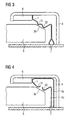
- FIG. 3 shows a first embodiment of the present invention.
- a contact spring 1 is arranged, which leads from an origin 7 to an abutment 6.
- the contact spring has two contact points 31, 32 on the contact surface 3b opposite a plug 5, which contacts the contact surface 3b as soon as the plug is pushed into the socket.
- the contact points 31, 32 lie on the continuous or integrally formed spring element 1. However, between the two contact points, a region of the spring which does not contact the contact surface 3b when the plug is inserted. Thus, two separate contact points are formed. It should be noted that the number of consecutive contact points on the spring element need not be limited to two. It can also be realized several consecutive contact points.
- the two contact points 31, 32 have different spring travel. That is, the contact points are different far away from the spring origin 7. This guarantees that they have a different resonant frequency and, in this respect, begin to vibrate at different vibrations and possibly lose contact with the contact surface. Due to the different spring travel, which come about by the spring geometry, it is ensured in this way that at least one contact point 31, 32 per contact spring has contact at the contact surface.
- FIG. 4 shows a further embodiment in which the contact spring 1 is divided into two legs 1a and 1b, that is, the spring is not continuous, but in several parts.
- the two legs 1a and 1b have a different Geometry and a different length.
- the two legs 1 a and 1 b each have a contact point 31, 32 for contacting the contact surface 3 b of the plug 5 to be inserted.
- the different lengths of the respective legs of the contact spring, the contact points have different properties again in this case so that they could lose contact with the plug or its contact surface with different vibrations or vibrations.
- the advantages of the present invention reside in the fact that different resonance frequencies of the individual contact points in the event of vibrations lead to the fact that always a contact is maintained, as well as by the use of multiple contact points generally greater contact reliability.
- the latter is particularly important in contamination of a contact point or a contact point of importance, as there are still more contact points or points are available and so the contact is ensured.
Landscapes
- Connector Housings Or Holding Contact Members (AREA)
- Coupling Device And Connection With Printed Circuit (AREA)
Abstract
Description
- Die Erfindung betrifft eine Kontaktfeder zum Herstellen eines elektrischen Kontakts mit einer Kontaktfläche und/oder einem Kontaktmesser, wobei die Kontaktfeder mindestens zwei Kontaktpunkte aufweist.
- Zur Herstellung eines elektrischen Kontaktes bei Stecksystemen werden in der Regel so genannte Kontaktfedern verwendet. Dies sind bei modernen Stecksystemen in der Regel schmale, längliche metallene Elemente, welche innerhalb einer Buchse, beispielsweise eines Ethernet-Steckers, angeordnet sind. In der Regel sind mehrere dieser Kontaktfedern parallel angeordnet, um gegenüber dem einzuschiebenden Stecker einen guten Kontakt zu ermöglichen. Auf der Steckerseite ist dann entsprechend eine den Kontaktfedern gegenüberliegende Kontaktfläche angebracht. In der Regel weisen derartige Kontaktfedern spezielle Stellen auf, an denen der Kontakt zwischen der Kontaktfeder und der gegenüberliegenden Kontaktfläche bzw. dem entsprechenden Kontaktmesser ausgebildet werden soll.
- Speziell im industriellen Umfeld ist nun besonders wichtig, dass ein einmal entstandener Kontakt bei Einschieben des Steckers nicht durch eventuelle vorkommende mechanische Beanspruchung gelöst werden kann. Insbesondere ist darauf zu achten, dass bei Erschütterungen der Kontakt bestehen bleibt.
- Die Aufgabe der vorliegenden Erfindung besteht daher darin, eine verbesserte Kontakteigenschaft einer Kontaktfeder anzugeben.
- Die Aufgabe wird durch die in Anspruch 1 angegebenen Merkmale gelöst.
- Die Idee hierbei ist insbesondere, dass eine Kontaktfeder, welche an unterschiedlichen Stellen spezielle Kontaktpunkte aufweist, einen verbesserten Kontakt herstellen kann. Hierbei sind die Kontaktpunkte an der Kontaktfeder so angebracht, dass sie jeweils unterschiedliche Federwege aufweisen. Das heißt, die Federgeometrie ist so gestaltet, dass an unterschiedlichen Stellen der Feder parallel zum Kontaktmesser bzw. zur Kontaktfläche Kontakt aufgenommen wird, sobald ein Stecker in die Buchse eingeschoben wird. Die unterschiedlichen Federwege von dem Befestigungspunkt bzw. dem Ursprung der Kontaktfeder zu den an der Kontaktfeder angeordneten Kontaktpunkten sorgen dafür, dass die Kontaktpunkte sich bei unterschiedlichen Frequenzen unterschiedlich verhalten. Die beiden Kontaktpunkte haben unterschiedliche Resonanzfrequenzen, so dass bei einer Erschütterung in der Regel mindestens einer der Kontaktpunkte mit der Kontaktfläche in Berührung bleibt.
- Die Kontaktfeder kann hierbei, wie im ersten Ausführungsbeispiel dargestellt, als eine durchgängige Kontaktfeder ausgebildet sein, welche an unterschiedlichen Entfernungen von ihrer Befestigung hintereinander angeordnet Kontaktpunkte zur Kontaktierung der Kontaktfläche aufweist. Hierbei ist zwischen den einzelnen Kontaktpunkten jeweils ein Bereich, in dem die Kontaktfeder keine Berührung mit der zu kontaktierenden Kontaktfläche aufnimmt. Es können hierbei mehrere derartige Kontaktpunkte hintereinander auf der Kontaktfeder angeordnet sein.
- Ein weiteres Ausführungsbeispiel ist dadurch gekennzeichnet, dass die Kontaktfeder ausgehend von ihrem Ursprung zwei Schenkel aufweist, welche jeweils eine unterschiedliche Länge aufweisen und welche jeweils an ihrem Schenkelende einen Kontaktpunkt aufweisen. Hierbei sind durch die unterschiedliche Länge der beiden Kontaktfederschenkel ebenfalls unterschiedliche Resonanzeigenschaften der beiden Kontaktpunkte gegeben, so dass bei Erschütterung jeweils einer der beiden Kontaktpunkte auf der Kontaktfläche anliegen bleibt.
- Eine Menge derartig ausgestalteter Federn wird beispielsweise in einer Kontaktbuchse, wie sie ebenfalls Gegenstand der Erfindung ist, parallel angebracht, so dass der eingeschobene Stecker an vielen Stellen über die entsprechenden Kontaktfedern kontaktiert wird.
- Damit ist ein sicherer Kontakt in einem Stecksystem gewährleistet.
- Im Folgenden wird die Erfindung anhand der Figuren näher beschrieben und erläutert.
- Es zeigen:
- FIG 1
- einen Stand der Technik,
- FIG 2
- einen Stand der Technik,
- FIG 3
- ein Ausführungsbeispiel mit durchgängiger Kontaktfeder,
- FIG 4
- ein Ausführungsbeispiel mit nicht durchgängiger Kontaktfeder.
-
FIG 1 zeigt ein Kontaktmesser 2, welches über eine Kontaktfeder 1 kontaktiert wird. Die Kontaktfeder weist zwei Schenkel auf, welche über die Kontaktpunkte 3 mit dem Kontaktmesser Kontakt aufnehmen. Die beiden Schenkel sind geometrisch gleichförmig, so dass sie ein gleichförmiges Verhalten aufweisen bei Erschütterung. Beide Schenkel würden bei der gleichen Frequenz anfangen zu vibrieren und entsprechend würden die Kontaktpunkte den Kontakt zum Kontaktmesser 2 verlieren. -
FIG 2 zeigt eine Buchse 4 eines Stecksystems. In der Buchse ist eine Kontaktfeder 1 angeordnet, welche einen Kontaktpunkt 3 aufweist, der auf eine Kontaktfläche 3b eines Steckers kontaktiert. Die Feder ist innerhalb der Buchse 4 an einem Widerlager 6 gelagert und besitzt einen Ursprung 7. Die Kontaktfeder 1 weist einen Kontaktpunkt 3 auf, der zwar über einen längeren Weg der Feder ausgebildet ist, jedoch insgesamt nur einen Kontaktpunkt darstellt. -
FIG 3 zeigt ein erstes Ausführungsbeispiel der vorliegenden Erfindung. In einer Buchse 4 ist eine Kontaktfeder 1 angeordnet, welche von einem Ursprung 7 an ein Widerlager 6 führt. Die Kontaktfeder weist an der einem Stecker 5 gegenüberliegenden Kontaktfläche 3b jeweils zwei Kontaktpunkte 31, 32 auf, welche mit der Kontaktfläche 3b Kontakt aufnehmen, sobald der Stecker in die Buchse geschoben wird. Die Kontaktpunkte 31, 32 liegen auf dem durchgängig bzw. einteilig ausgebildeten Federelement 1. Hierbei ist zwischen den beiden Kontaktpunkten jedoch ein Bereich der Feder, welche die Kontaktfläche 3b nicht kontaktiert bei eingeschobenem Stecker. Es werden somit zwei getrennte Kontaktpunkte ausgebildet. Hierbei sei bemerkt, dass die Anzahl der auf dem Federelement hintereinander liegenden Kontaktpunkte nicht auf zwei beschränkt sein muss. Es können ebenso mehrere hintereinander liegende Kontaktpunkte realisiert werden. - Wichtig bei der vorliegenden Erfindung ist der Aspekt, dass die beiden Kontaktpunkte 31, 32 unterschiedliche Federwege aufweisen. Das heißt, die Kontaktpunkte sind unterschiedlich weit vom Federursprung 7 entfernt. Dies garantiert, dass sie eine unterschiedliche Resonanzfrequenz aufweisen und diesbezüglich bei unterschiedlichen Vibrationen anfangen, entsprechend zu schwingen und gegebenenfalls den Kontakt zur Kontaktfläche zu verlieren. Durch die unterschiedlichen Federwege, welche durch die Federgeometrie zustande kommen, ist auf diese Weise gewährleistet, dass mindestens jeweils ein Kontaktpunkt 31, 32 pro Kontaktfeder an der Kontaktfläche Kontakt hat.
-
FIG 4 zeigt ein weiteres Ausführungsbeispiel, bei dem die Kontaktfeder 1 in zwei Schenkel 1a und 1b aufgeteilt ist, d.h. die Feder ist nicht durchgängig ausgebildet, sondern mehrteilig. Die beiden Schenkel 1a und 1b weisen eine unterschiedliche Geometrie und eine unterschiedliche Länge auf. An ihrem Ende haben die beiden Schenkel 1a und 1b jeweils einen Kontaktpunkt 31, 32 zur Kontaktierung der der Feder gegenüber liegenden Kontaktfläche 3b des einzuschiebenden Steckers 5. Durch die unterschiedliche Länge der jeweiligen Schenkel der Kontaktfeder weisen die Kontaktpunkte auch in diesem Fall wieder unterschiedliche Eigenschaften auf, so dass sie bei unterschiedlichen Vibrationen bzw. Erschütterungen den Kontakt zum Stecker bzw. dessen Kontaktfläche verlieren könnten. Somit ist auch in diesem Fall gewährleistet, dass immer einer der Kontaktpunkte 31, 32 Kontakt zur entsprechenden Kontaktfläche aufweist. - Zusammenfassend sind die Vorteile der vorliegenden Erfindung darin zu sehen, dass unterschiedliche Resonanzfrequenzen der einzelnen Kontaktpunkte bei auftretenden Vibrationen dazu führen, dass immer ein Kontakt erhalten bleibt, sowie durch die Verwendung mehrerer Kontaktpunkte allgemein eine größere Kontaktsicherheit. Letzteres ist insbesondere bei Verunreinigung einer Kontaktstelle bzw. eines Kontaktpunktes von Bedeutung, da immer noch weitere Kontaktstellen bzw. -punkte vorhanden sind und so der Kontakt sichergestellt ist.
Claims (4)
- Kontaktfeder (1) zum Herstellen eines elektrischen Kontakts mit einer Kontaktfläche (3b) und/oder einem Kontaktmesser (2), wobei die Kontaktfeder (1) mindestens zwei Kontaktpunkte (31, 32) aufweist,
dadurch gekennzeichnet, dass
die Kontaktfeder (1) zwischen den Kontaktpunkten (31, 32) und dem Ursprung (7) der Kontaktfeder jeweils unterschiedliche Federwege aufweist. - Kontaktfeder nach Anspruch 1, wobei die Kontaktpunkte (31, 32) aufeinander folgend an der durchgängig ausgebildeten Kontaktfeder (1) angeordnet sind und wobei die Kontaktfeder (1) zwischen den Kontaktpunkten (31, 32) mindestens einen Bereich (0) aufweist, der nicht zur Kontaktherstellung dient.
- Kontaktfeder nach Anspruch 1, wobei die Kontaktpunkte (31, 32) auf unterschiedlichen Schenkeln der mehrteilig ausgebildeten Kontaktfeder (1) angeordnet sind, wobei die Schenkel (la, 1b) eine unterschiedliche Länge und/oder Form aufweisen und wobei zwischen den Kontaktpunkten (31, 32) keine Federverbindung besteht.
- Buchse für ein Stecksystem mit einer oder mehreren Kontaktfedern (1) nach einem der Ansprüche 1 bis 3.
Priority Applications (2)
| Application Number | Priority Date | Filing Date | Title |
|---|---|---|---|
| EP20070005800 EP1973202B1 (de) | 2007-03-21 | 2007-03-21 | Kontaktsystem mit mehrfacher Kontaktauflage |
| CN2008100857620A CN101308967B (zh) | 2007-03-21 | 2008-03-20 | 具有多个接触支撑位置的接触系统 |
Applications Claiming Priority (1)
| Application Number | Priority Date | Filing Date | Title |
|---|---|---|---|
| EP20070005800 EP1973202B1 (de) | 2007-03-21 | 2007-03-21 | Kontaktsystem mit mehrfacher Kontaktauflage |
Publications (2)
| Publication Number | Publication Date |
|---|---|
| EP1973202A1 true EP1973202A1 (de) | 2008-09-24 |
| EP1973202B1 EP1973202B1 (de) | 2013-06-19 |
Family
ID=38130712
Family Applications (1)
| Application Number | Title | Priority Date | Filing Date |
|---|---|---|---|
| EP20070005800 Ceased EP1973202B1 (de) | 2007-03-21 | 2007-03-21 | Kontaktsystem mit mehrfacher Kontaktauflage |
Country Status (2)
| Country | Link |
|---|---|
| EP (1) | EP1973202B1 (de) |
| CN (1) | CN101308967B (de) |
Cited By (2)
| Publication number | Priority date | Publication date | Assignee | Title |
|---|---|---|---|---|
| WO2014028266A1 (en) * | 2012-08-15 | 2014-02-20 | Tyco Electronics Corporation | Electrical contact |
| EP2717283A1 (de) | 2012-10-02 | 2014-04-09 | ABB Technology AG | Elektrische Schaltvorrichtung mit mehreren Nennkontakten und Verfahren zu Herstellung der elektrischen Schaltvorrichtung |
Citations (2)
| Publication number | Priority date | Publication date | Assignee | Title |
|---|---|---|---|---|
| FR2568423A3 (fr) | 1984-07-27 | 1986-01-31 | Philips Nv | Element de contact electrique. |
| EP0390070A2 (de) | 1989-03-28 | 1990-10-03 | Mitsubishi Denki Kabushiki Kaisha | Elektrodenkonstruktion für eine Batterie in einem elektrischen Gerät |
Family Cites Families (1)
| Publication number | Priority date | Publication date | Assignee | Title |
|---|---|---|---|---|
| CH504770A (de) * | 1970-01-26 | 1971-03-15 | Holzer Patent Ag | Kontaktanordnung an einem Nockenschalter, insbesondere zur Verwendung in Programmschaltwerken |
-
2007
- 2007-03-21 EP EP20070005800 patent/EP1973202B1/de not_active Ceased
-
2008
- 2008-03-20 CN CN2008100857620A patent/CN101308967B/zh not_active Expired - Fee Related
Patent Citations (2)
| Publication number | Priority date | Publication date | Assignee | Title |
|---|---|---|---|---|
| FR2568423A3 (fr) | 1984-07-27 | 1986-01-31 | Philips Nv | Element de contact electrique. |
| EP0390070A2 (de) | 1989-03-28 | 1990-10-03 | Mitsubishi Denki Kabushiki Kaisha | Elektrodenkonstruktion für eine Batterie in einem elektrischen Gerät |
Cited By (3)
| Publication number | Priority date | Publication date | Assignee | Title |
|---|---|---|---|---|
| WO2014028266A1 (en) * | 2012-08-15 | 2014-02-20 | Tyco Electronics Corporation | Electrical contact |
| US9033750B2 (en) | 2012-08-15 | 2015-05-19 | Tyco Electronics Corporation | Electrical contact |
| EP2717283A1 (de) | 2012-10-02 | 2014-04-09 | ABB Technology AG | Elektrische Schaltvorrichtung mit mehreren Nennkontakten und Verfahren zu Herstellung der elektrischen Schaltvorrichtung |
Also Published As
| Publication number | Publication date |
|---|---|
| CN101308967B (zh) | 2012-06-06 |
| EP1973202B1 (de) | 2013-06-19 |
| CN101308967A (zh) | 2008-11-19 |
Similar Documents
| Publication | Publication Date | Title |
|---|---|---|
| DE102014207206A1 (de) | Elektrischer Draht-Verbindungsstruktur und elektrischer Draht Verbindungsverfahren | |
| DE202018104493U1 (de) | Elektrische Kontaktfelder mit Verlängerungen | |
| DE102020132430A1 (de) | Elektrische Anschlussanordnung mit Verbindungshalter | |
| DE102014108965A1 (de) | Einzelelement-Verbinder Draht zu Platte | |
| EP2976812A1 (de) | Elektrischer litzenleiter mit rundsteckkontaktbuchse | |
| EP2812949A1 (de) | Elektrischer steckverbinder zur elektrischen verbindung mittels ultraschallschweissen | |
| DE102012213069A1 (de) | Leiterrahmen, Verfahren zum Herstellen einer Kontaktgruppe, und Verbinder | |
| EP1973202B1 (de) | Kontaktsystem mit mehrfacher Kontaktauflage | |
| DE202010016269U1 (de) | Statorstab | |
| DE102010012404A1 (de) | Phasenanschlussverbindungen für einen Stator mit Stabwicklungen | |
| DE202016102870U1 (de) | Hülse für einen Federkontaktstift | |
| EP0681343A2 (de) | Einrichtung zum Massenanschluss von elektrischen Kabeln, insbesondere an einer Kraftfahrzeug-Karosserie | |
| DE102018116599A1 (de) | Verfahren zum Verbinden eines elektrischen Leiters mit einem Kontaktelement | |
| DE112014004613T5 (de) | Deformierte gefaltete Dipolantenne | |
| WO2018153405A1 (de) | Steckverbindermodul mit federbrücken | |
| DE112014000454T5 (de) | Sicherungs-Einheit | |
| DE112016005773T5 (de) | Anschlusspassstück und Verbinder | |
| DE1260650B (de) | Elektromechanisches Filter | |
| EP2887461A1 (de) | Einpoliger elektrischer Verbinder mit hermaphroditischen Kontaktelementen | |
| DE2816532C3 (de) | Anschlußeinrichtung für einen elektrischen Steckverbinder | |
| DE102018207788B4 (de) | Kontaktelement und Kontaktanordnung zur Entlastung einer Lötstelle | |
| DE3024249A1 (de) | Anschlusselement fuer elektrische schaltdraehte | |
| DE102016007117A1 (de) | Kontaktlamelle für ein buchsenartiges Steckverbinderteil und buchsenartiges Steckverbinderteil | |
| DE202016100931U1 (de) | Sicherungssockel | |
| CH409044A (de) | Elektrische Verbindung zwischen einer Klemme mit Wendelteil und einem Leiter |
Legal Events
| Date | Code | Title | Description |
|---|---|---|---|
| PUAI | Public reference made under article 153(3) epc to a published international application that has entered the european phase |
Free format text: ORIGINAL CODE: 0009012 |
|
| AK | Designated contracting states |
Kind code of ref document: A1 Designated state(s): AT BE BG CH CY CZ DE DK EE ES FI FR GB GR HU IE IS IT LI LT LU LV MC MT NL PL PT RO SE SI SK TR |
|
| AX | Request for extension of the european patent |
Extension state: AL BA HR MK RS |
|
| 17P | Request for examination filed |
Effective date: 20090321 |
|
| 17Q | First examination report despatched |
Effective date: 20090420 |
|
| AKX | Designation fees paid |
Designated state(s): DE FR GB IT |
|
| GRAP | Despatch of communication of intention to grant a patent |
Free format text: ORIGINAL CODE: EPIDOSNIGR1 |
|
| RAP1 | Party data changed (applicant data changed or rights of an application transferred) |
Owner name: SIEMENS AKTIENGESELLSCHAFT |
|
| GRAS | Grant fee paid |
Free format text: ORIGINAL CODE: EPIDOSNIGR3 |
|
| GRAA | (expected) grant |
Free format text: ORIGINAL CODE: 0009210 |
|
| AK | Designated contracting states |
Kind code of ref document: B1 Designated state(s): DE FR GB IT |
|
| REG | Reference to a national code |
Ref country code: GB Ref legal event code: FG4D Free format text: NOT ENGLISH |
|
| REG | Reference to a national code |
Ref country code: DE Ref legal event code: R096 Ref document number: 502007011900 Country of ref document: DE Effective date: 20130814 |
|
| PLBE | No opposition filed within time limit |
Free format text: ORIGINAL CODE: 0009261 |
|
| STAA | Information on the status of an ep patent application or granted ep patent |
Free format text: STATUS: NO OPPOSITION FILED WITHIN TIME LIMIT |
|
| 26N | No opposition filed |
Effective date: 20140320 |
|
| REG | Reference to a national code |
Ref country code: DE Ref legal event code: R097 Ref document number: 502007011900 Country of ref document: DE Effective date: 20140320 |
|
| REG | Reference to a national code |
Ref country code: FR Ref legal event code: PLFP Year of fee payment: 10 |
|
| REG | Reference to a national code |
Ref country code: FR Ref legal event code: PLFP Year of fee payment: 11 |
|
| REG | Reference to a national code |
Ref country code: FR Ref legal event code: PLFP Year of fee payment: 12 |
|
| PGFP | Annual fee paid to national office [announced via postgrant information from national office to epo] |
Ref country code: GB Payment date: 20190313 Year of fee payment: 13 Ref country code: FR Payment date: 20190322 Year of fee payment: 13 Ref country code: IT Payment date: 20190327 Year of fee payment: 13 |
|
| PGFP | Annual fee paid to national office [announced via postgrant information from national office to epo] |
Ref country code: DE Payment date: 20190517 Year of fee payment: 13 |
|
| REG | Reference to a national code |
Ref country code: DE Ref legal event code: R119 Ref document number: 502007011900 Country of ref document: DE |
|
| PG25 | Lapsed in a contracting state [announced via postgrant information from national office to epo] |
Ref country code: FR Free format text: LAPSE BECAUSE OF NON-PAYMENT OF DUE FEES Effective date: 20200331 Ref country code: DE Free format text: LAPSE BECAUSE OF NON-PAYMENT OF DUE FEES Effective date: 20201001 |
|
| GBPC | Gb: european patent ceased through non-payment of renewal fee |
Effective date: 20200321 |
|
| PG25 | Lapsed in a contracting state [announced via postgrant information from national office to epo] |
Ref country code: GB Free format text: LAPSE BECAUSE OF NON-PAYMENT OF DUE FEES Effective date: 20200321 |
|
| PG25 | Lapsed in a contracting state [announced via postgrant information from national office to epo] |
Ref country code: IT Free format text: LAPSE BECAUSE OF NON-PAYMENT OF DUE FEES Effective date: 20200321 |