EP1967839A1 - Delay time modulated and femtosecond time-resolved, scanning probe microscope apparatus - Google Patents
Delay time modulated and femtosecond time-resolved, scanning probe microscope apparatus Download PDFInfo
- Publication number
- EP1967839A1 EP1967839A1 EP08011222A EP08011222A EP1967839A1 EP 1967839 A1 EP1967839 A1 EP 1967839A1 EP 08011222 A EP08011222 A EP 08011222A EP 08011222 A EP08011222 A EP 08011222A EP 1967839 A1 EP1967839 A1 EP 1967839A1
- Authority
- EP
- European Patent Office
- Prior art keywords
- delay time
- ultrashort laser
- laser pulses
- probe
- scanning probe
- Prior art date
- Legal status (The legal status is an assumption and is not a legal conclusion. Google has not performed a legal analysis and makes no representation as to the accuracy of the status listed.)
- Withdrawn
Links
- 239000000523 sample Substances 0.000 title claims abstract description 168
- 238000001514 detection method Methods 0.000 claims abstract description 35
- 230000005641 tunneling Effects 0.000 claims description 23
- 230000008859 change Effects 0.000 claims description 10
- 230000002123 temporal effect Effects 0.000 abstract description 23
- 230000001419 dependent effect Effects 0.000 abstract description 12
- 230000001443 photoexcitation Effects 0.000 abstract description 2
- 238000010586 diagram Methods 0.000 description 17
- 238000005259 measurement Methods 0.000 description 13
- 230000035945 sensitivity Effects 0.000 description 12
- 238000007493 shaping process Methods 0.000 description 11
- 229910001218 Gallium arsenide Inorganic materials 0.000 description 9
- 238000010276 construction Methods 0.000 description 8
- 230000036961 partial effect Effects 0.000 description 8
- 230000036962 time dependent Effects 0.000 description 8
- 230000003287 optical effect Effects 0.000 description 5
- 230000004044 response Effects 0.000 description 4
- 239000007787 solid Substances 0.000 description 4
- 230000004888 barrier function Effects 0.000 description 3
- 230000001678 irradiating effect Effects 0.000 description 3
- 238000000034 method Methods 0.000 description 3
- 239000010936 titanium Substances 0.000 description 3
- 238000007796 conventional method Methods 0.000 description 2
- 239000004973 liquid crystal related substance Substances 0.000 description 2
- 239000010445 mica Substances 0.000 description 2
- 229910052618 mica group Inorganic materials 0.000 description 2
- 239000010409 thin film Substances 0.000 description 2
- 230000001052 transient effect Effects 0.000 description 2
- RTAQQCXQSZGOHL-UHFFFAOYSA-N Titanium Chemical compound [Ti] RTAQQCXQSZGOHL-UHFFFAOYSA-N 0.000 description 1
- 238000010521 absorption reaction Methods 0.000 description 1
- 238000007792 addition Methods 0.000 description 1
- 230000004075 alteration Effects 0.000 description 1
- 239000000969 carrier Substances 0.000 description 1
- 230000003247 decreasing effect Effects 0.000 description 1
- 230000007547 defect Effects 0.000 description 1
- 239000000686 essence Substances 0.000 description 1
- 230000005284 excitation Effects 0.000 description 1
- 230000005281 excited state Effects 0.000 description 1
- 239000000835 fiber Substances 0.000 description 1
- 239000000463 material Substances 0.000 description 1
- 238000000691 measurement method Methods 0.000 description 1
- 230000009022 nonlinear effect Effects 0.000 description 1
- 239000010453 quartz Substances 0.000 description 1
- 230000002040 relaxant effect Effects 0.000 description 1
- 238000012552 review Methods 0.000 description 1
- 239000003362 semiconductor superlattice Substances 0.000 description 1
- VYPSYNLAJGMNEJ-UHFFFAOYSA-N silicon dioxide Inorganic materials O=[Si]=O VYPSYNLAJGMNEJ-UHFFFAOYSA-N 0.000 description 1
- 239000000758 substrate Substances 0.000 description 1
- 230000001360 synchronised effect Effects 0.000 description 1
- 229910052719 titanium Inorganic materials 0.000 description 1
Images


Classifications
-
- G—PHYSICS
- G01—MEASURING; TESTING
- G01J—MEASUREMENT OF INTENSITY, VELOCITY, SPECTRAL CONTENT, POLARISATION, PHASE OR PULSE CHARACTERISTICS OF INFRARED, VISIBLE OR ULTRAVIOLET LIGHT; COLORIMETRY; RADIATION PYROMETRY
- G01J3/00—Spectrometry; Spectrophotometry; Monochromators; Measuring colours
- G01J3/28—Investigating the spectrum
- G01J3/42—Absorption spectrometry; Double beam spectrometry; Flicker spectrometry; Reflection spectrometry
- G01J3/433—Modulation spectrometry; Derivative spectrometry
-
- G—PHYSICS
- G01—MEASURING; TESTING
- G01J—MEASUREMENT OF INTENSITY, VELOCITY, SPECTRAL CONTENT, POLARISATION, PHASE OR PULSE CHARACTERISTICS OF INFRARED, VISIBLE OR ULTRAVIOLET LIGHT; COLORIMETRY; RADIATION PYROMETRY
- G01J3/00—Spectrometry; Spectrophotometry; Monochromators; Measuring colours
- G01J3/28—Investigating the spectrum
- G01J3/2889—Rapid scan spectrometers; Time resolved spectrometry
-
- G—PHYSICS
- G01—MEASURING; TESTING
- G01N—INVESTIGATING OR ANALYSING MATERIALS BY DETERMINING THEIR CHEMICAL OR PHYSICAL PROPERTIES
- G01N21/00—Investigating or analysing materials by the use of optical means, i.e. using sub-millimetre waves, infrared, visible or ultraviolet light
- G01N21/62—Systems in which the material investigated is excited whereby it emits light or causes a change in wavelength of the incident light
- G01N21/63—Systems in which the material investigated is excited whereby it emits light or causes a change in wavelength of the incident light optically excited
- G01N21/64—Fluorescence; Phosphorescence
- G01N21/6408—Fluorescence; Phosphorescence with measurement of decay time, time resolved fluorescence
-
- G—PHYSICS
- G01—MEASURING; TESTING
- G01Q—SCANNING-PROBE TECHNIQUES OR APPARATUS; APPLICATIONS OF SCANNING-PROBE TECHNIQUES, e.g. SCANNING PROBE MICROSCOPY [SPM]
- G01Q30/00—Auxiliary means serving to assist or improve the scanning probe techniques or apparatus, e.g. display or data processing devices
- G01Q30/02—Non-SPM analysing devices, e.g. SEM [Scanning Electron Microscope], spectrometer or optical microscope
-
- G—PHYSICS
- G01—MEASURING; TESTING
- G01Q—SCANNING-PROBE TECHNIQUES OR APPARATUS; APPLICATIONS OF SCANNING-PROBE TECHNIQUES, e.g. SCANNING PROBE MICROSCOPY [SPM]
- G01Q60/00—Particular types of SPM [Scanning Probe Microscopy] or microscopes; Essential components thereof
- G01Q60/10—STM [Scanning Tunnelling Microscopy] or apparatus therefor, e.g. STM probes
- G01Q60/12—STS [Scanning Tunnelling Spectroscopy]
-
- G—PHYSICS
- G01—MEASURING; TESTING
- G01J—MEASUREMENT OF INTENSITY, VELOCITY, SPECTRAL CONTENT, POLARISATION, PHASE OR PULSE CHARACTERISTICS OF INFRARED, VISIBLE OR ULTRAVIOLET LIGHT; COLORIMETRY; RADIATION PYROMETRY
- G01J1/00—Photometry, e.g. photographic exposure meter
- G01J1/42—Photometry, e.g. photographic exposure meter using electric radiation detectors
- G01J2001/4242—Modulated light, e.g. for synchronizing source and detector circuit
-
- G—PHYSICS
- G01—MEASURING; TESTING
- G01N—INVESTIGATING OR ANALYSING MATERIALS BY DETERMINING THEIR CHEMICAL OR PHYSICAL PROPERTIES
- G01N21/00—Investigating or analysing materials by the use of optical means, i.e. using sub-millimetre waves, infrared, visible or ultraviolet light
- G01N21/62—Systems in which the material investigated is excited whereby it emits light or causes a change in wavelength of the incident light
- G01N21/63—Systems in which the material investigated is excited whereby it emits light or causes a change in wavelength of the incident light optically excited
- G01N21/64—Fluorescence; Phosphorescence
- G01N21/6408—Fluorescence; Phosphorescence with measurement of decay time, time resolved fluorescence
- G01N2021/6415—Fluorescence; Phosphorescence with measurement of decay time, time resolved fluorescence with two excitations, e.g. strong pump/probe flash
-
- G—PHYSICS
- G01—MEASURING; TESTING
- G01N—INVESTIGATING OR ANALYSING MATERIALS BY DETERMINING THEIR CHEMICAL OR PHYSICAL PROPERTIES
- G01N21/00—Investigating or analysing materials by the use of optical means, i.e. using sub-millimetre waves, infrared, visible or ultraviolet light
- G01N21/62—Systems in which the material investigated is excited whereby it emits light or causes a change in wavelength of the incident light
- G01N21/63—Systems in which the material investigated is excited whereby it emits light or causes a change in wavelength of the incident light optically excited
- G01N21/64—Fluorescence; Phosphorescence
- G01N21/645—Specially adapted constructive features of fluorimeters
- G01N21/6456—Spatial resolved fluorescence measurements; Imaging
- G01N21/6458—Fluorescence microscopy
-
- Y—GENERAL TAGGING OF NEW TECHNOLOGICAL DEVELOPMENTS; GENERAL TAGGING OF CROSS-SECTIONAL TECHNOLOGIES SPANNING OVER SEVERAL SECTIONS OF THE IPC; TECHNICAL SUBJECTS COVERED BY FORMER USPC CROSS-REFERENCE ART COLLECTIONS [XRACs] AND DIGESTS
- Y10—TECHNICAL SUBJECTS COVERED BY FORMER USPC
- Y10S—TECHNICAL SUBJECTS COVERED BY FORMER USPC CROSS-REFERENCE ART COLLECTIONS [XRACs] AND DIGESTS
- Y10S977/00—Nanotechnology
- Y10S977/84—Manufacture, treatment, or detection of nanostructure
- Y10S977/849—Manufacture, treatment, or detection of nanostructure with scanning probe
- Y10S977/85—Scanning probe control process
Definitions
- the present invention relates to an apparatus for measuring a physical phenomenon by photoexcitation, which has an ultimate resolution both temporal and spatial. More specifically, the invention relates to a delay time modulated and time-resolved, scanning probe microscope apparatus.
- a scanning probe microscope e.g., a scanning tunneling microscope
- a scanning tunneling microscope is an apparatus in which the probe apex having a radius of curvature in the order of angstroms is brought proximate to a surface of a specimen across a distance in the order of angstroms and a tunnel junction is formed between the probe apex and the specimen surface to measure a morphology of the surface on an atomic level from a tunneling current passing through the tunnel junction.
- the scanning tunneling microscope using a piezo stage that allows scanning with a precision in the order of angstroms, is capable of obtaining a surface morphology at an ultimate spatial resolution.
- an ultrashort laser pulse apparatus is an apparatus that is capable of producing a laser pulse having a full width of half maximum in the order of femtoseconds at an ultimate temporal resolution as short as femtoseconds.
- One such apparatus is a delay time modulated and time-resolved scanning probe microscope apparatus.
- a specimen disposed in a scanning probe microscope is irradiated with a series of ultrashort laser pulse pairs for exciting the specimen while the delay time between the two laser pulses in each pulse pair is varied, and the probe signal is measured as a function of the delay time.
- This apparatus with the ability to measure a transient response of a nanoscale local area to a photoexcited physical phenomenon allows deriving from it the knowledge of the photoexcited physical phenomenon that is needed in creating a functional device and an ultrafast device utilizing photophysical properties.
- the use of an ultrashort laser pulse capable of exciting a carrier in a small or nanoscale area in a specimen allows determining a lifetime of the carrier from a delay time dependency of a probe signal component that is dependent on the delay time.
- FIG. 9 shows such a construction of a conventional time-resolved scanning probe microscope apparatus.
- the scanning probe microscope is illustrated as being a scanning tunneling microscope.
- ultrashort laser pulses 62 at a given repetition rate from a ultrashort laser pulse generator 60 are split by an interferometric delay circuit 61 into two pulses 63 and 64 having a delay time t d of 1 ps (picosecond) or so.
- the pulses 63 and 64 are chopped by a chopper 65 with a frequency ⁇ to be incident on an area on a specimen which lies below a probe 66 in a tunneling microscope unit.
- a lock-in detection device 69 is used to lock-in-detect a tunneling current signal 67 using a frequency ⁇ (68) as a reference signal to find a difference signal I diff between a tunneling current I irr at the time of irradiation and a tunneling current I bak at the time of non-irradiation. This measurement is repeated while continuously changing the delay time t d between the ultrashort laser pulses 63 and 64 to determine the delay time dependency of the tunneling current component I diff that is dependent on the delay time.
- the probe signal component that is dependent on the delay time t d is much smaller than the component that is not dependent on the delay time t d , and cannot be measured with enough precision even if the dynamic range of the lock-in device is increased to its limit.
- the light output intensity of the ultrashort laser light pulse generator has a long-period fluctuation due to a small change in environment (such as temperature etc.) which fluctuation, however, cannot be eliminated by the conventional technique; hence it is hard to determine the delay time dependency of the probe signal at sufficient precision.
- the probe apex in the scanning probe microscope when irradiated with ultrafast laser pulses, is thermally elongated, while it shrinks when the laser pulses are turned off. This results in changes in the spacing between the probe apex and specimen surface and in turn in changes in the tunneling probability between them.
- the difficulty in measuring the delay time dependency of the probe signal at both high sensitivity and high precision.
- ultrashort laser pulses 63 and 64 having a delay time t d have an identical wavelength as shown in Fig. 9 .
- the relaxation time can be found by irradiating a specimen with a light pulse 74 having an energy corresponding to a difference in energy between the level 71 and the level 73 and a light pulse 75 having an energy corresponding to a difference in energy between the level 72 and the level 73 while continuously varying the delay time t d between these pulses and determining the delay time dependency of the probe signal component.
- the prior-art apparatus cannot have two short light pulses that have different wavelength to each other.
- a delay time modulated and femtosecond time-resolved scanning probe microscope apparatus characterized in that it comprises: an ultrashort laser pulse generator; a delay time modulating circuit for splitting an ultrashort light pulse produced by the said ultrashort laser pulse generator into two ultrashort laser pulses interspaced by a delay time while establishing a value for the delay time between the two ultrashort laser pulses and modulating the delay time centering about the established value with a fixed modulation frequency; a scanning probe microscope for scanning a specimen over a surface area thereof with a probe wherein the probe is disposed just above the specimen so that a tunnel junction is formed between a probe apex and a surface of the said specimen when irradiated with the said two ultrashort laser pulses modulated by the said delay time modulating circuit; and a lock-in detection unit for lock-in-detecting a probe signal of the specimen irradiated with the
- the said ultrashort laser pulse generator may be adapted to produce a series of ultrashort laser pulses having a pulse width in the order of femtoseconds at a fixed periodicity.
- the said delay time modulating circuit preferably includes a half mirror and two sets of movable mirrors of which each set comprises mirrors fastened to a piezo stage wherein at least one of the said sets of movable mirrors is adapted to be driven to change a center value of the delay time and to modulate the delay time as a center delay time with the fixed frequency.
- the said lock-in detection unit may be adapted to perform lock-in detection using the modulation frequency as a reference frequency.
- the ultrashort laser pulse generator produces at a fixed periodicity ultrashort laser pulses having a pulse width in the order of femtoseconds, each of which is split by a half mirror in the delay time modulating circuit into two ultrashort laser pulses. These two ultrashort laser pulses are reflected by two sets of movable mirrors fastened to a piezo stage, respectively, and then are again brought together through the half mirror.
- the delay time between the two ultrashort laser pulses is set at a desired value by adjusting the difference between the respective lengths of the turnaround optical paths with the two sets of movable mirrors, and the length of the optical path with one of the two sets of movable mirrors is modulated with a selected amplitude and a selected frequency.
- the two ultrashort laser pulses having the delay time modulated with the selected amplitude and frequency centering around the set delay time value are incident on the specimen just below the probe in the scanning probe microscope to change the energy state of the specimen, resulting in a change in the probe signal.
- the lock-in detection unit performs lock-in detection using the delay time modulation frequency as a reference frequency and detects a quantity that is proportional to the differential coefficient of the probe signal on the delay time between the two ultrashort laser pulses. The measurement is repeated by continuously changing the delay time.
- the ultrashort laser pulse generator provides a temporal resolution in the order of femtoseconds and the delay time modulating circuit uses a piezo stage, it is possible to set the delay time at a temporal resolution in the order of femtoseconds.
- the lock-in detection unit which uses the delay time modulation frequency as its reference frequency for lock-in detection detects the quantity that is proportional to the differential coefficient of the probe signal to the delay time between the ultrashort laser pulses, namely detecting the differential coefficient of the probe signal to the delay time between the ultrashort laser pulses directly, it is possible to measure at both high sensitivity and high precision a delay time dependent, minute component of the probe signal even if it contains a large background component.
- the delay time modulation frequency much higher than the frequency of fluctuations in intensity of ultrashort laser pulses allows a delay time dependent, minute component of the probe signal to be detected unaffected by such fluctuations in intensity of ultrashort laser pulses.
- the probe apex irradiating the specimen just below the probe with all the ultrashort laser pulses produced in a train by the ultrashort laser pulse generator at a fixed periodicity - rather than with those in part interrupted such as by a chopper as in the prior art - while making the frequency of ultrashort laser pulses produced much higher than the thermal response frequency at the probe apex permits the probe apex to be supplied with ultrashort light pulses continuously and with no time in which it is allowed to cool and thus to hold its temperature substantially constant. This will prevent the probe apex from repeatedly thermally expanding and contracting, prevent its distance from the surface of the specimen from changing and eventually prevent the tunneling probability from fluctuating.
- the use of the scanning probe providing a spatial resolution in the order of angstroms allows a delay time dependent, minute component of the probe signal to be detected at a spatial resolution in the order of angstroms, hence at both high sensitivity and high precision.
- a delay time modulated and femtosecond time resolved scanning probe microscope apparatus which comprises: an ultrashort laser pulse generator; an ultrabroadband, variable wavelength, multi-pulse waveform shaping unit (see PCT International Publication No. WO 01/44863 A1 ) for producing from an ultrashort laser pulse produced by the said ultrashort laser pulse generator, a plurality of ultrashort light pulses each of that can have different wavelength to others and interspaced by a delay time and establishing a desired value for the delay time between the ultrashort laser pulses different in wavelength; a wavelength/delay time/modulation timing control unit for producing a control signal to establish selected values for the wavelength of the ultrashort laser pulses, a control signal to establish a selected value for the delay time between the ultrashort laser pulses and a control signal to modulate the delay time at selected time instants, and delivering such control signals to a two-dimensional space amplitude modulator and a two-dimensional space phase modulator in the said ultrabroadband, variable wavelength
- the said wavelength/delay time/modulation timing control unit may be characterized in that it comprises a computer that is responsive to input values for desired wavelengths of and delay time between the said ultrashort laser pulses and an input value for a modulation timing frequency for computing control signals for the said two-dimensional space amplitude and phase modulators and transmitting these control signals thereto while furnishing the said lock-in detection unit with the said modulation timing signals.
- the said lock-in detection unit may be characterized in that it is configured to perform lock-in detection using the said modulation timing signals as a reference frequency and thereby to detect a quantity that is proportional to a differential coefficient of the said probe signal with respect to said delay time.
- the said scanning probe microscope may be characterized in that it is a scanning tunneling microscope or an atomic force microscope.
- a probe signal component that is dependent on a delay time between exciting light pulses at a spatial resolution in the order of angstroms and at a temporal resolution in the order of femtoseconds can be directly measured at both high sensitivity and high precision as with the delay time modulated and femtosecond time-resolved scanning microscope apparatus as set forth in claim 1.
- it permits a probe signal component that is dependent on a delay time between exciting light pulses different in wavelength and of wavelengths as desired to be directly measured at high sensitivity and precision. Accordingly, it makes it possible for a photoexcited physical phenomenon in which three or more energy levels take parts to be measured at an ultimate resolution both spatial and temporal.
- Fig. 1 is a diagram illustrating the construction of a delay time modulated and femtosecond time-resolved scanning probe microscope apparatus constituting a first form of implementation of the present invention.
- the delay time modulated and femtosecond time-resolved scanning probe microscope apparatus of the present invention designated by reference numeral 1 comprises an ultrashort laser pulse generator 2 for producing a series of ultrashort laser pulses 3; a delay time modulating circuit 6 which splits an ultrashort laser pulse 3 produced by the ultrashort laser pulse generator 2 into two ultrashort laser pulses 4 and 5 and which also modulates a delay time t d between ultrashort laser pulses 4 and 5 with a frequency ⁇ ; a scanning probe microscope 7 for scanning a specimen 18 over a surface area thereof with a probe 19 in which the probe 19 is disposed just above the specimen 18 so that a tunnel junction is formed between a probe 19's apex and the specimen 18 irradiated with the ultrashort laser pulses 4 and 5 with the delay
- reference numeral 9 is a CCD camera that aids in the setup of the scanning probe
- reference numerals 10 and 11 indicate the reference frequency ( ⁇ ) signal transmitted from the delay time modulating circuit 6 into the lock-in detection unit 8, and the probe signal transmitted from the scanning probe microscope 7 into the lock-in detection unit 8, respectively.
- Measurement data 12 are transmitted from the lock-in detection unit 8 into an image display (not shown) where they are displayed in the form of, e.g., what is indicated by reference numeral 13.
- the ultrashort laser pulse generator 2 produces an ultrashort laser pulse 3 having a pulse width in the order of femtoseconds recurrently at a fixed periodicity. It may be, for example, a Ti/sapphire laser that generates an ultrashort laser pulse of a wavelength of 800 nm (nanometer) and a pulse full width of half maximum of 25 fs (femtosecond) and at a repetition frequency of 80 MHz.
- the delay time modulating circuit 6 includes a half mirror 14 that splits the ultrashort laser pulse 3 into a first and a second ultrashort laser pulse 4 and 5 which travel respectively in a first and a second direction orthogonal to each other, and two sets of movable mirrors 15 and 16 provided in those directions in which the ultrashort laser pulses 4 and 5 travel, respectively.
- Each set of movable mirrors 15 and 16 can be driven by a piezo stage to adjust its spacing from the half mirror 14 as desired and also to oscillate with an amplitude as desired and at a frequency ( ⁇ ) as desired.
- the movable mirror 15 is used to adjust the center delay time t d (0) and the movable mirror 16 to apply the frequency modulation (with amplitude ⁇ t d and at frequency ⁇ ).
- the scanning probe microscope 7 may be one in which the probe 19's apex having a radius of curvature in the order of angstroms can be brought proximate to a specimen surface across a spacing in the order of angstroms and which is capable of scanning the specimen surface with a precision in the order of angstroms. It is preferably a scanning tunneling microscope or an atomic force microscope for very low temperature and ultrahigh vacuum using, e.g., a piezo stage.
- the lock-in detection unit may be a conventional one, preferably having a large dynamic range.
- the ultrashort laser pulse generator 2 produces an ultrashort laser pulse 3 having a pulse width in the order of femtoseconds recurrently at a fixed periodicity, and each ultrashort laser pulse 3 is split by the half mirror 14 in the delay time modulating circuit 6 into two ultrashort light pulses 4 and 5 which are separately reflected by the two sets of movable mirrors 15 and 16 and then brought together by the half mirror 14.
- the center delay time t d (0) between two ultrashort laser pulses 4 and 5 is set at a selected value by adjusting the difference between the turnaround optical path lengths with the movable mirror sets 15 and 16 while the optical path length with one movable mirror set 16 is modulated with a selected amplitude ⁇ t d and a selected frequency ⁇ .
- the two ultrashort laser pulses 4 and 5 with the delay time modulated with the selected amplitude ⁇ t d and the selected frequency ⁇ and centering around the center delay time t d (0) are incident on a gap 17 just below the probe in the scanning probe microscope 7 and change the energy state of the specimen 18, thereby changing the probe signal 11.
- the lock-in detection unit 8 performs lock-in detection using the modulation frequency ⁇ of the delay time as a reference frequency and detects a quantity that is proportional to a differential coefficient of the probe signal 11 with respect to the delay time (dI t /dt d ).
- t d t d 0 + o 2 ⁇ ⁇ t d ⁇ sin ⁇ ⁇ t and the lock-in detection with the reference frequency ⁇ gives rise to the detection of the coefficient of sin ⁇ t in the second term of the right side of equation (1), namely ⁇ ⁇ t d d I t d t d
- t d t d 0 .
- the ultrashort laser pulse generator 2 provides a temporal resolution of femtoseconds and the delay time modulating circuit 6 uses a piezo stage as mentioned above, it is here possible to set the delay time at a temporal resolution of femtoseconds.
- the lock-in detection unit 8 performs lock-in detection using the modulation frequency ⁇ as its reference frequency to directly detect a quantity that is proportional to a differential coefficient of the probe signal to the delay time with the result that fluctuating background components have been eliminated, the delay time dependency of the probe signal that is dependent on the delay time can be measured at a temporal resolution of femtoseconds, hence at both high sensitivity and high precision.
- the modulation frequency ⁇ of the delay time much higher than the fluctuation frequency of the ultrashort laser pulse intensity allows the delay time dependency of the probe signal to be measured unaffected by the fluctuation frequency of the ultrashort laser pulse intensity.
- a scanning probe microscope 7 providing a spatial resolution in the order of angstroms allows the measurement at a spatial resolution in the order of angstroms.
- This Example is to show that the apparatus of the present invention prevents the probe apex of a scanning probe from thermal expansion and shrinkage.
- Fig. 2 is a diagram illustrating results of measurement of the probe signal flowing through a Au (111) thin film deposited on mica in the present apparatus.
- the ultrashort laser pulse generator makes use of a Ti: sapphire laser that produces an ultrashort laser pulse having a wavelength of 800 nm and a pulse full width of half maximum of 25 fs recurrently at a repetition frequency of 80 MHz.
- Au is a material that does not exhibit absorption for a light wavelength of 800 nm and the probe signal is predicted not to fluctuate in a measurement.
- Fig. 2(a) is a graph showing the probe signal (tunnel current) as a function of time without the light irradiation, from which it is seen that the probe signal then does not change with time.
- Fig. 2(b) is a graph showing the probe signal that is measured when the laser light is chopped at a frequency of 200 Hz to irradiate, from which graph it is seen that the probe signal fluctuates at a cycle of 5 ms (millisecond), indicating that the probe apex of the scanning probe is thermally expanded and contracted by the laser pulse irradiation, thereby fluctuating the probe signal.
- Fig. 2(b) is a graph showing the probe signal that is measured when the laser light is chopped at a frequency of 200 Hz to irradiate, from which graph it is seen that the probe signal fluctuates at a cycle of 5 ms (millisecond), indicating that the probe apex of the scanning probe is thermally expanded and contracted by the laser pulse irradiation,
- 2(c) is a graph showing the probe signal that is measured when the delay time is modulated with a delay time modulation amplitude ⁇ t d of 400 fs and a modulation frequency ⁇ of 100 Hz, from which graph it is seen that the probe signal does not change with lapse of time. It is thus seen that the present apparatus does not cause the probe apex of the scanning probe to be thermally expanded and contracted by the laser pulse irradiation.
- FIG. 3 is a diagram showing a measurement system used to evaluate the temporal resolution of the present apparatus.
- the specimen was made of an n-type GaAs (100) substrate.
- the lifetime of the carrier of n-type GaAs is sufficiently long so that it may be little relaxed within a range of the delay time in this Example.
- Fig. 3(a) is a diagram showing an energy band structure made of the specimen 18 of n-type GaAs, the probe 19's apex and a gap 17 between the specimen 18 and the probe 19's apex.
- Fig. 3 is a diagram showing a measurement system used to evaluate the temporal resolution of the present apparatus.
- the specimen was made of an n-type GaAs (100) substrate.
- the lifetime of the carrier of n-type GaAs is sufficiently long so that it may be little relaxed within a range of the delay time in this Example.
- Fig. 3(a) is a diagram showing an energy band structure made of the specimen 18 of n-type
- 3(b) is a diagram showing the change of the probe signal (plotted along the ordinate axis) with respect to the bias voltage (plotted along the abscissa axis) which is applied between the probe 19's apex and the n-type GaAs 18 with the former taken as a basis in the makeup of Fig. 3(a) .
- the broken lines indicate the case without the light irradiation while the solid lines indicate the case where it is applied.
- the Schottky barrier that is formed at the tunneling gap is biased in the forward direction, which is followed by a rise in the tunneling probability such that electrons tunnel from the n-type GaAs 18 into the probe 19's apex and probe signal flows from the latter into the former.
- This state corresponds to what the broken curve in the region of negative voltage in Fig. 3(b) indicates. If the voltage is positive, as shown by the broken lines in Fig. 3(a) the existence of the energy barrier near the surface of the n-type GaAs 18 holds the tunneling probability small so that no probe signal flows into the n-type GaAs 18 from the probe 19's apex.
- This state corresponds to what is indicated by the broken line in the region of positive voltage in Fig. 3(b) . If the light irradiation is applied when the voltage is positive, carriers are then excited as indicated by the black solid arrow in Fig. 3(a) to make thinner the energy barrier near the surface of the n-type GaAs 18, which is followed by a rise in the tunneling probability such that electrons tunnel from the n-type GaAs 18 into the probe apex 19 and probe signal flows from the latter into the former.
- This state corresponds to what the solid curve indicates (as the black solid arrow points) in the region of positive voltage in Fig. 3(b) .
- Fig. 4 is a graph showing a temporal resolution of the present apparatus.
- the probe signal oscillates with a cycle of 2.68 fs corresponding to a wavelength of 800 nm of the ultrashort laser pulses that the probe signal oscillates responsive to interference intensities of the two ultrashort laser pulses. It is also seen that the entire envelope has a full width of half maximum of about 30 fs that corresponds to the pulse width of the ultrashort laser pulses. From these results it is seen that the present apparatus makes it possible to control the delay time at a precision of 1 fs.
- Fig. 4(b) is a graph of the quantity of the probe signal (the amount expressed by equation 2 mentioned above) that is proportional to the differential coefficient of the probe signal, which was measured by the same condition as in Fig.4 (a) where the delay time was modulated with an amplitude ⁇ t d of 0.5 fs and a modulation frequency ⁇ of 400 Hz. It is seen that the waveform of Fig. 4(b) assumes a differential waveform of the waveform of Fig. 4(a) . To wit, it is seen that the present apparatus allows the delay time dependent probe signal, namely the delay time dependent probe signal to be measured at a precision of 1 fs.
- the present apparatus is capable of measuring the delay time dependency of the probe signal at a temporal precision as short as a pulse width of ultrashort laser pulses.
- Fig. 5 is a diagram illustrating the construction of a delay time modulated and femtosecond time-resolved scanning probe microscope apparatus constituting such a second form of implementation of the present invention.
- the delay time modulated and femtosecond time-resolved scanning probe microscope apparatus of the invention in its second form of implementation is designated by reference character numeral 20 and is characterized by comprising an ultrashort laser pulse generator 21 for producing a series of ultrashort laser pulses 22; an ultrabroadband, variable wavelength, multi-pulse waveform shaping unit 25 which produces from an ultrashort laser pulse 22 produced by the ultrashort laser pulse generator 21, a plurality of ultrashort laser pulses 23 and 24 different in wavelength and interspaced by a delay time and which also is capable of establishing a desired value for the delay time between the ultrashort laser pulses 23 and 24 different in wavelength; a wavelength/delay time/modulation timing control unit 26 which produces a control signal 27 that sets up selected values for the wavelength of the ultrashort laser pulses
- reference numeral 12 indicates measurement data transmitted from the lock-in detection unit 8 to an image display 13.
- Fig. 6 is a diagram showing the makeup of the ultrabroadband, variable wavelength, multi-pulse waveform shaping unit. It corresponds to Fig. 1 contained in PCT International Publication No. WO 01/44863 A1 .
- the ultrabroadband, variable wavelength, multi-pulse waveform shaping unit 25 includes an ultrabroadband light pulse generator 31 which converts an ultrashort laser pulses 22 produced by the ultrashort laser pulse generator 21 into an ultrabroadband light pulse; a beam expander 35 which comprises a plurality of cylindrical lenses 32, 33 and a planar mirror 34 and by which the ultrashort laser pulse whose bandwidth is ultrabroadened is expanded in the direction of y-axis; a wavelength dispersing unit 38 which comprises a grating 36 and a cylindrical lens 37 curved in a direction of x-axis and by which the ultrashort laser pulse expanded in the direction of y-axis is collimated and its wavelengths are dispersed in the direction of x-axis; a two-dimensional space amplitude modulator 39 for setting a desired value for the transmissivity of each spot on an x-y plane of the collimated ultrashort laser pulse; a two-dimensional space phase modulator 40 for setting a desired value for the phase
- the ultrabroadband light pulse generator 31 utilizes a higher order nonlinear effect of a nonlinear optical medium and, if made of a tapered quartz fiber extremely thinned in its central part, is capable of widening the bandwidth of an ultrashort laser pulse generated at a high repetition rate by a titanium/sapphire laser (center wavelength 790 nm) from a bandwidth of 500 nm to a bandwidth of 1000 nm.
- the two-dimensional space amplitude modulator 39 is formed of an array of pixels made of a liquid crystal on an x-y plane in which the transmissivity of each pixcel can be selectively controlled by changing an applied voltage for each pixcel.
- the two-dimensional space phase modulator 40 as is the two-dimensional space amplitude modulator 39 is formed of an array of pixels made of a liquid crystal on an x-y plane in which the reflective index of each pixcel can be selectively controlled by changing an applied voltage for each pixcel.
- Fig. 7 diagrammatically illustrates an example of how the transmissivity of the two-dimensional space amplitude modulator 39 may be set.
- Fig. 7(a) shows an exemplary array of pixels arranged in four rows (y1, y2, y3 and y4) in a direction of y-axis and in twenty columns in a direction of x-axis in which pixels 51 shown in black represent those with their transmissivity set at 0 while pixels 52 shown in white represents those with their transmissivity set at desired values other than 0.
- Fig. 7(b) diagrammatically illustrates a spatial distribution of wavelengths and intensities of ultrashort laser pulses transmitted through the two-dimensional space amplitude modulator 39 in which transmissivities of pixels are set as shown in Fig. 7(a) .
- an ultrashort laser pulse incident on the two-dimensional space amplitude modulator 39 is expanded in a direction of y-axis and has its wavelengths dispersed in a direction of x-axis.
- the two-dimensional space amplitude modulator 39 is designed as shown in Fig.
- a single ultrashort laser pulse can be converted through the two-dimensional space amplitude modulator 39 into a plurality of ultrashort laser pulses varying in wavelength and spatially separated from one another as shown in Fig. 7(b) .
- Fig. 8 diagrammatically illustrates an example of how the phases can be set in the two-dimensional space phase modulator 40.
- Fig. 8(a) shows an exemplary array of pixels arranged in four rows (y1, y2, y3 and y4) in a direction of y-axis and in twenty columns in a direction of x-axis in which the successions of pixels 61 shown in white correspond, respectively in position, to a plurality of ultrashort laser pulses different in wavelength outgoing from the two-dimensional space amplitude modulator 39 to give them desired phases.
- Fig. 8(b) shows waveforms of ultrashort laser pulses on time axis (t) which are obtained when partial waves having desired different phases imparted thereto through different pixels 61 are brought together in a direction of x-axis.
- An ultrashort laser pulses output from the two-dimensional space amplitude modulator 39 is decomposed through pixels 61 of the two-dimensional space phase modulator 40 into partial waves each of which is then given a desired phase. Since imparting desired different phases to partial waves allows putting the partial waves side by side in a desired order on time axis, it is possible to output ultrashort laser pulses having a desired configuration on time axis. For example, it is possible to form two ultrashort laser pulses having a desired delay time t d on time axis as shown at row y1 in Fig. 8(b) from an ultrashort laser pulse as shown at row y1 in Fig.
- ultrashort laser pulses as shown respectively at rows y2 and y3 in Fig. 7(b) are decomposed into partial waves through the successive white pixels shown at rows y2 and y3 in Fig. 8(a) and these partial waves having desired phases imparted thereto are put side by side in a desired order on time axis
- the wavelength/delay time/modulation timing control unit 26 shown in Fig. 5 furnishes the space amplitude modulator 39 and the two-dimensional space phase modulator 40 with a modulation control signal 27 for bringing about a train of ultrashort laser pulses of a desired wavelength or wavelengths and a desired delay time or delay times. It further delivers, alternately with such a modulation control signal, another modulation control signal 27 at a fixed periodicity with which to vary only the delay time incrementally by an amount ⁇ t d expressed by Equation (1), thereby modulating the delay time t d at such a fixed periodicity. It also furnishes the lock-in detector 8 with timing signals (at a frequency ⁇ M) as the reference signal 28 to indicate delivery of each of modulation control signals time-delayed by ⁇ t d .
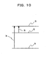
- a delay time modulated, femtosecond time-resolved scanning probe microscope apparatus in which wavelengths are selected for a plurality of ultrashort laser pulses, the delay time between such ultrashort laser pulses is varied and modulated at a fixed periodicity and a lock-in is detected with a delay time modulation frequency, it is possible to directly measure a quantity of the delay time dependent probe signal by irradiations with such a plurality of ultrashort laser pulses which vary in wavelength. According to this apparatus, it is possible to derive knowledge about a photoexcited physical phenomenon in which three or more energy levels are involved, for example, as shown in Fig. 10 .
- the present invention allows direct measurement of a probe signal component that is dependent on a delay time between ultrashort laser pulses and such measurement unaffected by a fluctuation in the intensity of ultrashort laser pulses, and prevents the probe apex from thermal expansion and shrinkage. It is thus made possible to measure a photoexcited physical phenomenon at a temporal resolution in the order of femtoseconds and at a spatial resolution in the order of angstroms. It is also made possible to directly measure a probe signal component that is dependent on a delay time between ultrashort laser pulses different in wavelength, which therefore allows acquisition of knowledge of a higher order photoexcited physical phenomenon.
- the present invention is extremely useful when used for the elucidation of a photoexcited physical phenomenon that occurs in a local area of nanoscale and in a time period in the order of femtoseconds.
Landscapes
- Physics & Mathematics (AREA)
- Spectroscopy & Molecular Physics (AREA)
- General Physics & Mathematics (AREA)
- Health & Medical Sciences (AREA)
- General Health & Medical Sciences (AREA)
- Nuclear Medicine, Radiotherapy & Molecular Imaging (AREA)
- Radiology & Medical Imaging (AREA)
- Life Sciences & Earth Sciences (AREA)
- Chemical & Material Sciences (AREA)
- Analytical Chemistry (AREA)
- Biochemistry (AREA)
- Immunology (AREA)
- Pathology (AREA)
- Investigating, Analyzing Materials By Fluorescence Or Luminescence (AREA)
- Investigating Or Analysing Materials By Optical Means (AREA)
- Microscoopes, Condenser (AREA)
Applications Claiming Priority (2)
| Application Number | Priority Date | Filing Date | Title |
|---|---|---|---|
| JP2001360047 | 2001-11-26 | ||
| EP02803925A EP1460410B1 (en) | 2001-11-26 | 2002-11-25 | Delay time modulation femtosecond time-resolved scanning probe microscope apparatus |
Related Parent Applications (1)
| Application Number | Title | Priority Date | Filing Date |
|---|---|---|---|
| EP02803925A Division EP1460410B1 (en) | 2001-11-26 | 2002-11-25 | Delay time modulation femtosecond time-resolved scanning probe microscope apparatus |
Publications (1)
| Publication Number | Publication Date |
|---|---|
| EP1967839A1 true EP1967839A1 (en) | 2008-09-10 |
Family
ID=19170940
Family Applications (2)
| Application Number | Title | Priority Date | Filing Date |
|---|---|---|---|
| EP02803925A Expired - Fee Related EP1460410B1 (en) | 2001-11-26 | 2002-11-25 | Delay time modulation femtosecond time-resolved scanning probe microscope apparatus |
| EP08011222A Withdrawn EP1967839A1 (en) | 2001-11-26 | 2002-11-25 | Delay time modulated and femtosecond time-resolved, scanning probe microscope apparatus |
Family Applications Before (1)
| Application Number | Title | Priority Date | Filing Date |
|---|---|---|---|
| EP02803925A Expired - Fee Related EP1460410B1 (en) | 2001-11-26 | 2002-11-25 | Delay time modulation femtosecond time-resolved scanning probe microscope apparatus |
Country Status (6)
| Country | Link |
|---|---|
| US (1) | US7002149B2 (da) |
| EP (2) | EP1460410B1 (da) |
| JP (1) | JP3796585B2 (da) |
| DE (1) | DE60228125D1 (da) |
| DK (1) | DK1460410T3 (da) |
| WO (1) | WO2003046519A1 (da) |
Families Citing this family (12)
| Publication number | Priority date | Publication date | Assignee | Title |
|---|---|---|---|---|
| JP2005014059A (ja) * | 2003-06-26 | 2005-01-20 | Ricoh Co Ltd | 超短パルスレーザ加工法及び加工装置並びに構造体 |
| JP4425098B2 (ja) * | 2004-09-06 | 2010-03-03 | 浜松ホトニクス株式会社 | 蛍光顕微鏡および蛍光相関分光解析装置 |
| US7420106B2 (en) * | 2005-03-18 | 2008-09-02 | The University Of Utah Research Foundation | Scanning probe characterization of surfaces |
| US7696479B2 (en) * | 2005-06-03 | 2010-04-13 | Massachusetts Institute Of Technology | Method and apparatus for frequency-converting infrared light |
| US7567876B2 (en) * | 2006-08-07 | 2009-07-28 | Vialogy Llc | Quantum resonance interferometry for detecting signals |
| JP4839481B2 (ja) * | 2006-11-29 | 2011-12-21 | 独立行政法人科学技術振興機構 | ポンププローブ測定装置及びそれを用いた走査プローブ顕微鏡装置 |
| US8064059B2 (en) * | 2008-11-04 | 2011-11-22 | Alipasha Vaziri | Optical pulse duration measurement |
| CN101806733B (zh) * | 2010-03-11 | 2011-11-09 | 中国科学院上海光学精密机械研究所 | 飞秒数字全息动态观察测量装置 |
| DE102012200858A1 (de) * | 2012-01-20 | 2013-07-25 | Freie Universität Berlin | Laserpulsformungsverfahren |
| CN111656164A (zh) * | 2018-01-19 | 2020-09-11 | 治疗诊断科技有限公司 | 扫描探头显微镜 |
| CN113655026B (zh) * | 2021-08-05 | 2024-01-23 | 中国科学院苏州生物医学工程技术研究所 | 椭半球曲面大视野高通量双光子显微镜 |
| CN114353686B (zh) * | 2021-09-10 | 2023-10-20 | 重庆交通大学 | 隧道衬砌的曲率分布智能获取方法及相关装置 |
Citations (1)
| Publication number | Priority date | Publication date | Assignee | Title |
|---|---|---|---|---|
| WO2001044863A1 (fr) | 1999-12-14 | 2001-06-21 | Japan Science And Technology Corporation | Dispositif de mise en forme de formes d'ondes d'impulsions multiplexees en longueurs d'ondes, a longueurs d'ondes variables, a bande ultra-large |
Family Cites Families (8)
| Publication number | Priority date | Publication date | Assignee | Title |
|---|---|---|---|---|
| EP0296262B1 (en) | 1987-06-22 | 1991-08-28 | International Business Machines Corporation | Method for investigating surfaces at nanometer and picosecond resolution and laser-sampled scanning tunneling microscope for performing said method |
| US4918319A (en) * | 1987-11-03 | 1990-04-17 | Puretan, Inc. | Tanning bed with closure control mechanism |
| US4980566A (en) * | 1989-08-02 | 1990-12-25 | The United States Of America As Represented By The Secretary Of Commerce | Ultrashort pulse multichannel infrared spectrometer apparatus and method for obtaining ultrafast time resolution spectral data |
| JP2743213B2 (ja) * | 1990-07-25 | 1998-04-22 | キヤノン株式会社 | 記録及び/又は再生を行なう装置および方法 |
| JP2744359B2 (ja) * | 1991-04-24 | 1998-04-28 | キヤノン株式会社 | 情報再生及び/又は情報記録装置 |
| US5416327A (en) * | 1993-10-29 | 1995-05-16 | Regents Of The University Of California | Ultrafast scanning probe microscopy |
| JP3200263B2 (ja) | 1993-11-11 | 2001-08-20 | シャープ株式会社 | 試料表面分析装置 |
| JP3145329B2 (ja) | 1997-02-03 | 2001-03-12 | 科学技術振興事業団 | 局所探査顕微鏡 |
-
2002
- 2002-11-25 DE DE60228125T patent/DE60228125D1/de not_active Expired - Lifetime
- 2002-11-25 EP EP02803925A patent/EP1460410B1/en not_active Expired - Fee Related
- 2002-11-25 US US10/496,571 patent/US7002149B2/en not_active Expired - Fee Related
- 2002-11-25 DK DK02803925T patent/DK1460410T3/da active
- 2002-11-25 EP EP08011222A patent/EP1967839A1/en not_active Withdrawn
- 2002-11-25 WO PCT/JP2002/012273 patent/WO2003046519A1/ja active IP Right Grant
- 2002-11-25 JP JP2003547911A patent/JP3796585B2/ja not_active Expired - Fee Related
Patent Citations (1)
| Publication number | Priority date | Publication date | Assignee | Title |
|---|---|---|---|---|
| WO2001044863A1 (fr) | 1999-12-14 | 2001-06-21 | Japan Science And Technology Corporation | Dispositif de mise en forme de formes d'ondes d'impulsions multiplexees en longueurs d'ondes, a longueurs d'ondes variables, a bande ultra-large |
Non-Patent Citations (6)
| Title |
|---|
| ANONYMOUS: "Time-Resolved Tunneling Microscope", IBM TECHNICAL DISCLOSURE BULLETIN, vol. 31, no. 11, 1 April 1989 (1989-04-01), New York, US, pages 350 - 352, XP000032531 * |
| FELDSTEIN M J ET AL: "Femtosecond optical spectroscopy and scanning probe microscopy", JOURNAL OF PHYSICAL CHEMISTRY ACS USA, vol. 100, no. 12, 21 March 1996 (1996-03-21), pages 4739 - 4748, XP002316523, ISSN: 0022-3654 * |
| HYOMEN-KAGAKU, SURFACE SCIENCE, vol. 20, pages 337 |
| JOURNAL OF APPLIED PHYSICS, vol. 83, no. 7, 1 April 1998 (1998-04-01), pages 3453 |
| JOURNAL OF APPLIED PHYSICS, vol. 88, no. 8, 15 October 2000 (2000-10-15), pages 4851 |
| SOLID STATE COMMUNICATIONS, vol. 6, no. 107, 1998, pages 281 |
Also Published As
| Publication number | Publication date |
|---|---|
| EP1460410A1 (en) | 2004-09-22 |
| DK1460410T3 (da) | 2008-12-08 |
| US7002149B2 (en) | 2006-02-21 |
| JPWO2003046519A1 (ja) | 2005-04-07 |
| WO2003046519A1 (en) | 2003-06-05 |
| JP3796585B2 (ja) | 2006-07-12 |
| EP1460410A4 (en) | 2005-04-06 |
| US20050035288A1 (en) | 2005-02-17 |
| EP1460410B1 (en) | 2008-08-06 |
| DE60228125D1 (de) | 2008-09-18 |
Similar Documents
| Publication | Publication Date | Title |
|---|---|---|
| EP2741072B1 (en) | Pump-probe measurement device and method | |
| EP1460410B1 (en) | Delay time modulation femtosecond time-resolved scanning probe microscope apparatus | |
| EP2090880B1 (en) | Pump probe measuring device, and scanning probe microscope apparatus using the device | |
| US6008899A (en) | Apparatus and method for optical pulse measurement | |
| US4972423A (en) | Method and apparatus for generating ultrashort light pulses | |
| JP5341488B2 (ja) | テラヘルツ波を測定するための装置及び方法 | |
| EP1662296A1 (en) | Optical control device and optical control method | |
| US20100187208A1 (en) | Laser pulse synthesis system | |
| EP3438625B1 (en) | Pulsed light waveform measurement method and waveform measurement device | |
| Osipov et al. | Nature of relaxation processes revealed by the action signals of intensity-modulated light fields | |
| JP4631704B2 (ja) | 半導体デバイスの電界分布測定方法と装置 | |
| Adachi et al. | Optical sampling four-wave-mixing experiment for exciton relaxation processes | |
| US6356381B1 (en) | Multi-wavelength cross-correlator for ultrashort radiation pulses | |
| JP2005072103A (ja) | レーザー周波数安定化装置、及びレーザー周波数安定化方法 | |
| JP7129099B2 (ja) | 走査プローブ顕微鏡、測定方法 | |
| JP4753063B2 (ja) | 光電場波形制御方法および制御装置 | |
| SU1074239A1 (ru) | Сканирующий лазерный микроскоп | |
| WO2008029187A2 (en) | Bandwidth-independent method and setup for detecting and stabilizing carrier-envelope phase drift of laser pulses by means of spectrally and spatially resolved interferometry | |
| EP4105645B1 (en) | Light detection device and light detection method | |
| Tortora et al. | Comb-like supercontinuum generation in bulk media | |
| CN116774468B (zh) | 光学脉冲输出序列的控制装置及控制方法 | |
| JP2005055652A (ja) | 可変スペクトル光発生装置 | |
| Urmancheev et al. | Photon echo area theorem for optically dense media | |
| Ozyazici et al. | An Autocorrelation Technique for Pulse Width Measurement of Ultrashort Optical Pulses. | |
| Dunn | Developing terahertz sources for characterising GaN semiconductor structures |
Legal Events
| Date | Code | Title | Description |
|---|---|---|---|
| PUAI | Public reference made under article 153(3) epc to a published international application that has entered the european phase |
Free format text: ORIGINAL CODE: 0009012 |
|
| 17P | Request for examination filed |
Effective date: 20080620 |
|
| AC | Divisional application: reference to earlier application |
Ref document number: 1460410 Country of ref document: EP Kind code of ref document: P |
|
| AK | Designated contracting states |
Kind code of ref document: A1 Designated state(s): DE DK FR GB |
|
| 17Q | First examination report despatched |
Effective date: 20081208 |
|
| AKX | Designation fees paid |
Designated state(s): DE DK FR GB |
|
| STAA | Information on the status of an ep patent application or granted ep patent |
Free format text: STATUS: THE APPLICATION IS DEEMED TO BE WITHDRAWN |
|
| 18D | Application deemed to be withdrawn |
Effective date: 20180602 |