EP1959567A2 - Vorrichtung und Verfahren zum Reduzieren einer spannungsabhängigen kapazitiven Kopplung - Google Patents
Vorrichtung und Verfahren zum Reduzieren einer spannungsabhängigen kapazitiven Kopplung Download PDFInfo
- Publication number
- EP1959567A2 EP1959567A2 EP08001060A EP08001060A EP1959567A2 EP 1959567 A2 EP1959567 A2 EP 1959567A2 EP 08001060 A EP08001060 A EP 08001060A EP 08001060 A EP08001060 A EP 08001060A EP 1959567 A2 EP1959567 A2 EP 1959567A2
- Authority
- EP
- European Patent Office
- Prior art keywords
- semiconductor substrate
- boundary layer
- layer
- doping concentration
- conductive
- Prior art date
- Legal status (The legal status is an assumption and is not a legal conclusion. Google has not performed a legal analysis and makes no representation as to the accuracy of the status listed.)
- Withdrawn
Links
Images


Classifications
-
- H—ELECTRICITY
- H03—ELECTRONIC CIRCUITRY
- H03H—IMPEDANCE NETWORKS, e.g. RESONANT CIRCUITS; RESONATORS
- H03H9/00—Networks comprising electromechanical or electro-acoustic elements; Electromechanical resonators
- H03H9/02—Details
- H03H9/02007—Details of bulk acoustic wave devices
- H03H9/02086—Means for compensation or elimination of undesirable effects
- H03H9/02125—Means for compensation or elimination of undesirable effects of parasitic elements
-
- H—ELECTRICITY
- H10—SEMICONDUCTOR DEVICES; ELECTRIC SOLID-STATE DEVICES NOT OTHERWISE PROVIDED FOR
- H10P—GENERIC PROCESSES OR APPARATUS FOR THE MANUFACTURE OR TREATMENT OF DEVICES COVERED BY CLASS H10
- H10P30/00—Ion implantation into wafers, substrates or parts of devices
- H10P30/20—Ion implantation into wafers, substrates or parts of devices into semiconductor materials, e.g. for doping
- H10P30/202—Ion implantation into wafers, substrates or parts of devices into semiconductor materials, e.g. for doping characterised by the semiconductor materials
- H10P30/204—Ion implantation into wafers, substrates or parts of devices into semiconductor materials, e.g. for doping characterised by the semiconductor materials into Group IV semiconductors
-
- H—ELECTRICITY
- H10—SEMICONDUCTOR DEVICES; ELECTRIC SOLID-STATE DEVICES NOT OTHERWISE PROVIDED FOR
- H10P—GENERIC PROCESSES OR APPARATUS FOR THE MANUFACTURE OR TREATMENT OF DEVICES COVERED BY CLASS H10
- H10P30/00—Ion implantation into wafers, substrates or parts of devices
- H10P30/20—Ion implantation into wafers, substrates or parts of devices into semiconductor materials, e.g. for doping
- H10P30/21—Ion implantation into wafers, substrates or parts of devices into semiconductor materials, e.g. for doping of electrically active species
-
- H—ELECTRICITY
- H10—SEMICONDUCTOR DEVICES; ELECTRIC SOLID-STATE DEVICES NOT OTHERWISE PROVIDED FOR
- H10P—GENERIC PROCESSES OR APPARATUS FOR THE MANUFACTURE OR TREATMENT OF DEVICES COVERED BY CLASS H10
- H10P30/00—Ion implantation into wafers, substrates or parts of devices
- H10P30/20—Ion implantation into wafers, substrates or parts of devices into semiconductor materials, e.g. for doping
- H10P30/28—Ion implantation into wafers, substrates or parts of devices into semiconductor materials, e.g. for doping characterised by an annealing step, e.g. for activation of dopants
Definitions
- the present invention relates to a device and a method for reducing a voltage dependent capacitive coupling.
- BAW filters and/or BAW resonators formed on a semiconductor base material are passive electrical RF devices usually operated in the gigahertz range.
- BAW resonators exemplarily comprise a bottom electrode and a top electrode separated by a piezoelectric layer and, when applying the resonant frequency, the result will be standing acoustic waves in the BAW resonator.
- the result will be resonance in the high-frequency band (usually in the gigahertz range). Due to the high frequency, a series of capacitive couplings which are usually undesired and are to be avoided may occur. Examples of this are capacitive couplings between individual conductive tracks or capacitive couplings relative to an electrode of the BAW filter or even via an electrically conductive substrate material.
- Capacitive couplings between pads or conductive tracks can, for example, be minimized by a suitable design of pads and conductive tracks.
- Another way is using a high-resistance semiconductor material (such as, for example, lightly doped semiconductor material) as the substrate material so that capacitive coupling between metal layers via the substrate material can be avoided due to the high electrical resistances of the substrate.
- a disadvantage resulting from using a lightly doped semiconductor material is, for example, a voltage-dependent substrate capacitance C(U) occurring between metallic patterns in the BAW filter and the substrate.
- the voltage-dependent substrate capacitance C(U) is generated by the surface effect at metal-oxide semiconductor (MOS) interfaces or boundary surfaces, as is known from MOS transistors.
- Embodiments of the present invention comprise a device with a first means for separating a conductive layer from a semiconductor substrate and a second means for reducing a voltage dependent capacitive coupling between the conductive layer and the semiconductor substrate.
- Embodiments of the present invention relate to a device for reducing a voltage dependent capacitive coupling between a conductive layer and a semiconductor substrate, the device comprising an insulating layer and the insulating layer electrically separating the conductive layer and the semiconductor substrate.
- the device comprises a boundary layer arranged between the insulating layer and the semiconductor substrate.
- the boundary layer comprises an electrically conductive material or a semiconductor material, the semiconductor material comprising a doping concentration that is higher than a doping concentration of the semiconductor substrate.
- the boundary layer comprises a lateral extension and hence is formed two-dimensionally on a surface, for example facing the insulating layer, of the semiconductor substrate with a layer thickness.
- the layer thickness of the boundary layer is selected such that a lateral area charge density corresponds at least to a breakdown charge density of the semiconductor substrate. It is, however, of advantage if the layer thickness is significant bigger, e.g. up to the 10 3 -fold thereof.
- the boundary layer can be arranged on the semiconductor substrate by forming a separate layer on the surface of the semiconductor substrate. Alternatively, the boundary layer may be arranged in the semiconductor substrate by doping the surface up to a depth corresponding to the layer thickness of the boundary layer.
- the layer thickness can be, e.g., around or less than 100 nm, around or less than 1 ⁇ m or several microns (e.g. less than 100 ⁇ m).
- the doping concentration of the boundary layer should be significantly higher than a possible doping concentration of the semiconductor substrate (e.g. by at least one order of magnitude).
- the boundary layer may be patterned such that it substantially "mirrors" the conductive layer, i.e. the boundary layer comprises a planar dimension, which corresponds substantially to a planar dimension of the conductive layer and the relative lateral position of both layers agrees to an accuracy of less than 40% or better less than 10%.
- the boundary layer is patterned such that it extends between the conductive layer and the semiconductor substrate with a tolerance of, for example, +/- 40% or better +/-10%.
- This arrangement of the boundary is of advantage, since different structures and/or other devices, which are integrated in the semiconductor substrate, remain electrically separated (thereby avoiding for example of short circuits).
- Further embodiments comprise a plurality of conductive layers and a plurality of boundary layers so that each boundary layer is associated with one conductive layer of the plurality of conductive layers.
- the conductive layer is part of a high frequency device.
- the conductive layer comprises, for example, a bottom electrode of a BAW resonator, which in addition comprises a piezoelectric layer and a further conductive layer (e.g. a top electrode) that are formed on the conductive layer.
- the BAW resonator is formed such that the conductive layer and the further conductive layer are separated by the piezoelectric layer, wherein the further conductive layer and the conductive layer may comprise a metal, such as aluminum or tungsten (or may even comprise several layers).
- the conductive layer includes a conductive track or a contact pad providing an electrical contact for a device.
- Embodiments of the present invention also include a method of reducing a voltage dependent capacitive coupling.
- the method includes the steps of providing a boundary layer comprising a conductive material or a doped semiconductor material, wherein the doping may include tempering.
- the method may comprise a structuring of the boundary layer, wherein the structuring includes, for example, using a photolithographic technique with a mask.
- the boundary layer may be produced by a heavily doped region (N ⁇ 10 20 cm -3 ) in a lightly doped semiconductor base material (N ⁇ 10 14 cm -3 ).
- a heavily doped region N ⁇ 10 20 cm -3
- a lightly doped semiconductor base material N ⁇ 10 14 cm -3
- the heavy doping concentration is located directly at an interface between the substrate wafer surface and insulator material above it (for example silicon oxide). Attention should be paid to the depth of the heavy doping concentration in the substrate wafer. This means specifically that the depth of doping being low in order to minimize the capacitive coupling between the doping zones, i.e. between the boundary layer and the semiconductor substrate.
- a lower limit of the depth can be obtained again from the lateral area charge density, which can be calculated as an integral of the doping along the doping profile into the substrate up to the depth of the doping.
- the lateral area charge density should again considerably exceed the breakdown charge of around 2*10 12 cm -2 required for silicon.
- Embodiments of the present invention thus comprise patterned heavily doped regions below the metal structures of the exemplary BAW filters and serve as suppression of the voltage-dependent capacity.
- the substrate is tempered, i.e. subjected to a suitable temperature to electrically activate the dopants.
- the subsequent layers of the BAW resonator are set up and patterned in another process flow.
- the boundary layer is produced by forming an additional semiconductor layer on the semiconductor substrate, wherein the additional semiconductor layer comprises a doping concentration, which obeys same limitations as explained before for the boundary layer.
- Embodiments of the present invention thus offer an improvement in filter characteristics of a BAW (bulk acoustic wave) filter formed on a semiconductor base material by producing locally heavily doped regions below pads, conductive tracks and resonators and, in addition, offer the advantage of efficiently suppressing voltage dependent capacitive couplings in an MOS structure, which can be really disturbing in particular in high-frequency range applications and.
- the advantage achieved by this is obtained particularly with a simple process management and thus at low cost.
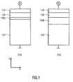
- Fig. 1 shows a cross-sectional view of an MOS structure along an xz-plane including a conductive layer 110, an insulating layer 130 and a semiconductor substrate 120.
- a voltage V 1 is applied to the conductive layer 110
- a voltage V 2 is applied to the conductive layer 110, wherein the semiconductor substrate 120 in both cases is at ground.
- a depletion zone (space charge zone) 150 develops between the insulating layer 130 and the semiconductor substrate 120, when a voltage is applied.
- Fig. 1 shows a depletion zone
- first voltage V 1 is smaller than the second voltage V 2 , and consequently a second depletion zone 150b in Fig. 1b along the z-direction is increased compared to a first depletion zone 150a in Fig. 1a .
- the depletion zones 150 thus are voltage-dependent and evolve at the MOS interface (as a consequence of the field effect).
- the insulating layer 130 and the depletion zone 150 make contributions to the capacitance C between the conductive layer 110 and the semiconductor substrate 120.
- the contributions come from the insulating layer 130 (C SiO2 ) and the depletion zones 150a, 150b (C RLZ ). Since the depletion zones 150a, 150b are more or less developed depending on an applied voltage the capacitance C is voltage-dependent. Specifically, this means that the following applies for the capacitances: C V 1 > C V 2 .
- the voltage dependent depletion zone 150 comprises a voltage dependent capacitive coupling between the conductive layer 110 und the semiconductor substrate 120. Especially if a high-frequency signal is attached to the conductive layer 110, this is a disturbing feature.
- Fig. 2 shows a cross-sectional view of a device for reducing the voltage dependent capacitive coupling between the conductive layer 110 and the semiconductor substrate 120, which are separated by the insulating layer 130.
- What is shown is a cross-sectional view along the xz-plane, wherein the z-direction is perpendicular to a layer plane (xy-plane) in which the conductive layer 110 and the insulating layer 130 are arranged on the semiconductor substrate 120.
- the insulating layer 130 and the semiconductor substrate 120 are separated from each other by a boundary layer 140.
- the boundary layer 140 comprises a doped semiconductor material having a higher doping concentration when compared to the semiconductor substrate.
- the insulating layer 130 serves as an electrical insulation of the conductive layer 110 from the semiconductor material 120 or the boundary layer 140.
- the boundary layer 140 is patterned such that its extension in the xy-plane nearly coincides with an extension of the conductive layer 110 in this plane, wherein a tolerance of +/- 40% or preferably +/- 10% may occur.
- Exemplary materials for the conductive layer 110 are aluminum and silicon oxide for the insulating layer 130.
- the doping of the surface should be of the same type as the doping of the semiconductor substrate 120. If the semiconductor substrate 120 is, for example, p-doped silicon, the boundary layer 140 should be highly p-doped silicon.
- doping materials exhibit specific advantages in the process of forming the boundary layer 140 of a specific thickness.
- a doping with Phosphorus will usually remain at the surface in the tempering process, which is performed to activate the dopants. This simplifies the process of forming the boundary layer 140 with a small thickness.
- doping with boron requires more effort in order to ensure the specific thickness. A reason for this is, that boron atoms very quickly migrate into an interior region of the semiconductor substrate 120 in the tempering process.
- Figs. 3a and 3b show cross-sectional views of a layer sequence for an embodiment of the present invention which, as is the case in Figs. 1a and 1b , comprise the conductive layer 110, the semiconductor substrate 120 and the insulating layer 130.
- the boundary layer 140 which is not present in Figs. 1a and 1b is formed in the layer sequence of Figs. 3a and 3b .
- the effect of the boundary layer 140 is that when applying a voltage V no voltage-dependent depletion zone forms in the semiconductor substrate 120, more explicitly the depletion zone is voltage-independent.
- the capacitive coupling between the conductive layer 110 and the semiconductor substrate 120 is also voltage-independent.
- a voltage V 1 is applied to the conductive layer 110 which is smaller than a voltage V 2 applied to the conductive layer 110 in Fig. 3b .
- the semiconductor substrate 120 is at ground.
- the capacitance C(V 1 ) of the layer sequence of Fig. 3a obtains contributions from a capacitance of the insulating layer (C Sio2 ) and a capacitance of the depletion zone (C RLZ (V 1 )).
- the surface doping with a high concentration as given by the boundary layer 140 provides a nearly voltage-independent depletion zone at the MOS interface. This is an important feature of the layout in Fig. 3 (in contrast to the layout in Fig. 1 ), especially if a high-frequency signal is applied to the conductive layer 110.
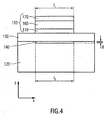
- Fig. 4 shows an embodiment in which the conductive layer 110 is a bottom electrode of a BAW resonator 155.
- the conductive layer 110 in turn is formed on an insulating layer 130, wherein the insulating layer 130 is formed on a semiconductor substrate 120 along an xy-plane (the y-direction here is perpendicular to the plane of the drawing of Fig. 4 ).
- a piezoelectric layer 160 and a further conductive layer 170 are formed on conductive layer 110, the piezoelectric layer 160 separating the conductive layer 110 and the further conductive layer 170.
- the conductive layer 110 forms a bottom electrode and the further conductive layer 170 forms a top electrode of the BAW resonator 155.
- the BAW resonator extends over a first length l 1 (an extension of the BAW resonator along the y-direction is not shown in this cross-sectional view).
- the boundary layer 140 is formed below the BAW resonator 155 (in a negative z-direction) and extends over a second length 1 2 along the x-direction.
- the lateral extension of the conductive layer 110 corresponds to the extension of the boundary layer 140, which implies that a center position of the conductive layer 110 agrees with a center position of the boundary layer 140 as well as the first length 1 1 agrees the second length 1 2 with a tolerance of +/- 30% and, preferably, +/- 10% (i.e. the boundary layer 140 comprises around the same size with no lateral shift compared to the BAW resonator).
- the boundary layer 140 comprises around the same size with no lateral shift compared to the BAW resonator.
- a length and position adjustment takes place for an extension along the y-direction, which is not shown in Fig. 4 .
- the extension of the boundary layer 140, 1 2 may be selected to be slightly greater than the first extension 1 1 to suppress capacitive coupling of the conductive layer 110 to the semiconductor substrate 120 more effectively.
- This will particularly apply for the case that neighboring devices/structures in the semiconductor substrate 120 are not influenced by the boundary layer 140 (for example, when they are in a greater lateral distance). Otherwise, the length 1 2 is chosen such, that negative interferences with the neighboring devices are minimized.
- the BAW resonator 155 comprises only an example for a RF-device (high-frequency device) and in a more general case, the conductive layer 110 is part of the RF-device and comprises, for example, an electrode for the RF-device or is connected to one.
- the boundary layer 140 comprises a layer thickness d which is generally selected to be as small as possible to suppress capacitive coupling between the boundary layer 140 and the semiconductor substrate 120.
- the layer thickness d of the boundary layer 140 which is given by the fact that an area charge density with regard to the xy-area of the boundary layer 140 corresponds to at least a breakdown charge density of the semiconductor substrate 120.
- the breakdown charge density is about 2*10 12 cm -2 .
- the lateral area charge density of the boundary layer 140 corresponds to the doping concentration.
- the minimal value of the layer thickness d thus, on one hand, depends on the doping of the boundary layer 140 and, on the other hand, on the semiconductor substrate or, more precisely, on its breakdown charge density. Summarizing, the two conditions for the layer thickness d, there is a lower threshold value given by the breakdown charge density of the semiconductor substrate 120 and an upper threshold for the layer thickness d is given by a suppression of a capacitive coupling between the boundary layer 140 and the semiconductor substrate 120.
- the boundary layer 140 is not only formed below a BAW resonator 155 but also below conductive tracks or terminal pads.
- the conductive tracks may, for example, contact the bottom electrode of the BAW resonator.
- the boundary layer 140 is patterned so that it will basically only exist below the conductive layer 110, which in the absent of the boundary layer 140 exhibits a voltage dependent capacitive coupling to the underlying semiconductor substrate 120. If the boundary layer 140 is formed by a heavily doped region of semiconductor substrate, the heavily doped region should have the same type of doping as the underlying semiconductor substrate 120 (if doped). Thus, a (parasitic) pn junction between the boundary layer 140 and the semiconductor substrate 120 is avoided.
- the boundary layer 140 can also comprise a further (highly doped) semiconductor layer, an equipotential floating layer (as for example a metal) or other material with a high enough charge density, so that that the area charge exceeds the breakdown charge, as explained above. Since metals comprise extreme high charge density, the thickness d of the boundary layer 140 can be chosen very small. Also for these alternatives, the boundary layer 140 is formed on the surface of the semiconductor substrate 120 preferably such that the extension and location of the conductive layer 110 and the boundary layer 140 correspond to each other.
Landscapes
- Physics & Mathematics (AREA)
- Acoustics & Sound (AREA)
- Piezo-Electric Or Mechanical Vibrators, Or Delay Or Filter Circuits (AREA)
- Semiconductor Integrated Circuits (AREA)
Applications Claiming Priority (1)
| Application Number | Priority Date | Filing Date | Title |
|---|---|---|---|
| US11/706,558 US8188548B2 (en) | 2007-02-15 | 2007-02-15 | Device and method for reducing a voltage dependent capacitive coupling |
Publications (2)
| Publication Number | Publication Date |
|---|---|
| EP1959567A2 true EP1959567A2 (de) | 2008-08-20 |
| EP1959567A3 EP1959567A3 (de) | 2013-07-17 |
Family
ID=39402594
Family Applications (1)
| Application Number | Title | Priority Date | Filing Date |
|---|---|---|---|
| EP08001060.6A Withdrawn EP1959567A3 (de) | 2007-02-15 | 2008-01-21 | Vorrichtung und Verfahren zum Reduzieren einer spannungsabhängigen kapazitiven Kopplung |
Country Status (2)
| Country | Link |
|---|---|
| US (1) | US8188548B2 (de) |
| EP (1) | EP1959567A3 (de) |
Families Citing this family (1)
| Publication number | Priority date | Publication date | Assignee | Title |
|---|---|---|---|---|
| WO2009113013A2 (en) * | 2008-03-14 | 2009-09-17 | Nxp B.V. | A sensor device and a method of detecting particles |
Citations (1)
| Publication number | Priority date | Publication date | Assignee | Title |
|---|---|---|---|---|
| US20050237132A1 (en) | 2004-04-20 | 2005-10-27 | Kabushiki Kaisha Toshiba | Film bulk acoustic-wave resonator and method for manufacturing the same |
Family Cites Families (6)
| Publication number | Priority date | Publication date | Assignee | Title |
|---|---|---|---|---|
| JPH10150185A (ja) * | 1996-11-20 | 1998-06-02 | Mitsubishi Electric Corp | 半導体装置及びその製造方法 |
| US6496085B2 (en) * | 2001-01-02 | 2002-12-17 | Nokia Mobile Phones Ltd | Solidly mounted multi-resonator bulk acoustic wave filter with a patterned acoustic mirror |
| FR2852165A1 (fr) * | 2003-03-06 | 2004-09-10 | St Microelectronics Sa | Procede de realisation d'un microresonateur piezolectrique accordable |
| US7332985B2 (en) * | 2003-10-30 | 2008-02-19 | Avago Technologies Wireless Ip (Singapore) Pte Ltd. | Cavity-less film bulk acoustic resonator (FBAR) devices |
| WO2007026397A1 (ja) * | 2005-08-30 | 2007-03-08 | Kyocera Corporation | 圧電共振素子及びそれを用いた圧電共振装置 |
| JP2008172713A (ja) * | 2007-01-15 | 2008-07-24 | Hitachi Media Electoronics Co Ltd | 圧電薄膜共振器および圧電薄膜共振器フィルタおよびその製造方法 |
-
2007
- 2007-02-15 US US11/706,558 patent/US8188548B2/en not_active Expired - Fee Related
-
2008
- 2008-01-21 EP EP08001060.6A patent/EP1959567A3/de not_active Withdrawn
Patent Citations (1)
| Publication number | Priority date | Publication date | Assignee | Title |
|---|---|---|---|---|
| US20050237132A1 (en) | 2004-04-20 | 2005-10-27 | Kabushiki Kaisha Toshiba | Film bulk acoustic-wave resonator and method for manufacturing the same |
Also Published As
| Publication number | Publication date |
|---|---|
| US8188548B2 (en) | 2012-05-29 |
| US20080197423A1 (en) | 2008-08-21 |
| EP1959567A3 (de) | 2013-07-17 |
Similar Documents
| Publication | Publication Date | Title |
|---|---|---|
| US8120142B2 (en) | Applying trenched transient voltage suppressor (TVS) technology for distributed low pass filters | |
| US8101494B2 (en) | Structure, design structure and method of manufacturing a structure having VIAS and high density capacitors | |
| US7989905B2 (en) | MEMS device having a movable electrode | |
| JP5209301B2 (ja) | 混合信号についての基板クロストークを低減する技術及びrf回路設計 | |
| KR102011942B1 (ko) | 고전압 레지스터 디바이스 | |
| EP2015353A1 (de) | Halbleiterbauelement und herstellungsverfahren dafür | |
| KR19980044524A (ko) | 기판 변환기술을 이용한 인덕터 소자 및 그 제조 방법 | |
| US20180269296A1 (en) | Semiconductor Device Including a Gate Contact Structure | |
| US20090283859A1 (en) | Integrated Circuit Arrangements With ESD-Resistant Capacitor and Corresponding Method of Production | |
| US8957496B2 (en) | Integrated circuit chip with discontinuous guard ring | |
| EP2544241A2 (de) | Feldeffekttransistor mit isoliertem Gate, der ein Dummy-Gate aufweist | |
| US8722475B2 (en) | Method and structure for high Q varactor | |
| EP1959567A2 (de) | Vorrichtung und Verfahren zum Reduzieren einer spannungsabhängigen kapazitiven Kopplung | |
| US7323749B2 (en) | Semiconductor device comprising an integrated circuit | |
| WO2010001352A1 (en) | Improved meander resistor | |
| JP5026257B2 (ja) | 電子装置 | |
| US7598825B2 (en) | Flap resonator, method of manufacturing a flap resonator, and integrated circuit including the flap resonator | |
| JP2014107417A (ja) | 半導体装置 | |
| US20050017362A1 (en) | Low gate resistance layout procedure for RF transistor devices | |
| US8125013B2 (en) | Structure, design structure and method of manufacturing a structure having VIAS and high density capacitors | |
| US20250220934A1 (en) | Trench Capacitor and Method for Manufacturing the Same | |
| KR101559911B1 (ko) | 금속 배선 형태의 인덕터 하부에 mim 캐패시터를 상기 배선의 폭보다 크지 않게 접목시키는 lc 회로 제조방법 | |
| US20160351710A1 (en) | Three Dimensional Monolithic LDMOS Transistor | |
| US8102010B2 (en) | Apparatus for reducing parasitic capacitance in a semiconductor device | |
| CN118043969A (zh) | 瞬态电压吸收元件 |
Legal Events
| Date | Code | Title | Description |
|---|---|---|---|
| PUAI | Public reference made under article 153(3) epc to a published international application that has entered the european phase |
Free format text: ORIGINAL CODE: 0009012 |
|
| AK | Designated contracting states |
Kind code of ref document: A2 Designated state(s): AT BE BG CH CY CZ DE DK EE ES FI FR GB GR HR HU IE IS IT LI LT LU LV MC MT NL NO PL PT RO SE SI SK TR |
|
| AX | Request for extension of the european patent |
Extension state: AL BA MK RS |
|
| PUAL | Search report despatched |
Free format text: ORIGINAL CODE: 0009013 |
|
| AK | Designated contracting states |
Kind code of ref document: A3 Designated state(s): AT BE BG CH CY CZ DE DK EE ES FI FR GB GR HR HU IE IS IT LI LT LU LV MC MT NL NO PL PT RO SE SI SK TR |
|
| AX | Request for extension of the european patent |
Extension state: AL BA MK RS |
|
| RIC1 | Information provided on ipc code assigned before grant |
Ipc: H03H 9/02 20060101AFI20130611BHEP |
|
| 17P | Request for examination filed |
Effective date: 20140116 |
|
| RBV | Designated contracting states (corrected) |
Designated state(s): AT BE BG CH CY CZ DE DK EE ES FI FR GB GR HR HU IE IS IT LI LT LU LV MC MT NL NO PL PT RO SE SI SK TR |
|
| AKX | Designation fees paid |
Designated state(s): AT BE BG CH CY CZ DE DK EE ES FI FR GB GR HR HU IE IS IT LI LT LU LV MC MT NL NO PL PT RO SE SI SK TR |
|
| STAA | Information on the status of an ep patent application or granted ep patent |
Free format text: STATUS: THE APPLICATION IS DEEMED TO BE WITHDRAWN |
|
| 18D | Application deemed to be withdrawn |
Effective date: 20170801 |