EP1959493A1 - Process for producing electronic part, process for producing heat conducting member, and method of mounting heat conducting member for electronic part - Google Patents
Process for producing electronic part, process for producing heat conducting member, and method of mounting heat conducting member for electronic part Download PDFInfo
- Publication number
- EP1959493A1 EP1959493A1 EP05814186A EP05814186A EP1959493A1 EP 1959493 A1 EP1959493 A1 EP 1959493A1 EP 05814186 A EP05814186 A EP 05814186A EP 05814186 A EP05814186 A EP 05814186A EP 1959493 A1 EP1959493 A1 EP 1959493A1
- Authority
- EP
- European Patent Office
- Prior art keywords
- bonding material
- thermosetting adhesive
- conductive member
- heat conductive
- substrate
- Prior art date
- Legal status (The legal status is an assumption and is not a legal conclusion. Google has not performed a legal analysis and makes no representation as to the accuracy of the status listed.)
- Granted
Links
Images

Classifications
-
- H—ELECTRICITY
- H10—SEMICONDUCTOR DEVICES; ELECTRIC SOLID-STATE DEVICES NOT OTHERWISE PROVIDED FOR
- H10W—GENERIC PACKAGES, INTERCONNECTIONS, CONNECTORS OR OTHER CONSTRUCTIONAL DETAILS OF DEVICES COVERED BY CLASS H10
- H10W76/00—Containers; Fillings or auxiliary members therefor; Seals
- H10W76/10—Containers or parts thereof
-
- H—ELECTRICITY
- H10—SEMICONDUCTOR DEVICES; ELECTRIC SOLID-STATE DEVICES NOT OTHERWISE PROVIDED FOR
- H10W—GENERIC PACKAGES, INTERCONNECTIONS, CONNECTORS OR OTHER CONSTRUCTIONAL DETAILS OF DEVICES COVERED BY CLASS H10
- H10W95/00—Packaging processes not covered by the other groups of this subclass
-
- H—ELECTRICITY
- H10—SEMICONDUCTOR DEVICES; ELECTRIC SOLID-STATE DEVICES NOT OTHERWISE PROVIDED FOR
- H10W—GENERIC PACKAGES, INTERCONNECTIONS, CONNECTORS OR OTHER CONSTRUCTIONAL DETAILS OF DEVICES COVERED BY CLASS H10
- H10W40/00—Arrangements for thermal protection or thermal control
- H10W40/70—Fillings or auxiliary members in containers or in encapsulations for thermal protection or control
-
- H—ELECTRICITY
- H10—SEMICONDUCTOR DEVICES; ELECTRIC SOLID-STATE DEVICES NOT OTHERWISE PROVIDED FOR
- H10W—GENERIC PACKAGES, INTERCONNECTIONS, CONNECTORS OR OTHER CONSTRUCTIONAL DETAILS OF DEVICES COVERED BY CLASS H10
- H10W76/00—Containers; Fillings or auxiliary members therefor; Seals
- H10W76/10—Containers or parts thereof
- H10W76/12—Containers or parts thereof characterised by their shape
- H10W76/15—Containers comprising an insulating or insulated base
- H10W76/153—Containers comprising an insulating or insulated base having interconnections in passages through the insulating or insulated base
-
- H—ELECTRICITY
- H10—SEMICONDUCTOR DEVICES; ELECTRIC SOLID-STATE DEVICES NOT OTHERWISE PROVIDED FOR
- H10W—GENERIC PACKAGES, INTERCONNECTIONS, CONNECTORS OR OTHER CONSTRUCTIONAL DETAILS OF DEVICES COVERED BY CLASS H10
- H10W72/00—Interconnections or connectors in packages
- H10W72/071—Connecting or disconnecting
- H10W72/072—Connecting or disconnecting of bump connectors
- H10W72/07251—Connecting or disconnecting of bump connectors characterised by changes in properties of the bump connectors during connecting
-
- H—ELECTRICITY
- H10—SEMICONDUCTOR DEVICES; ELECTRIC SOLID-STATE DEVICES NOT OTHERWISE PROVIDED FOR
- H10W—GENERIC PACKAGES, INTERCONNECTIONS, CONNECTORS OR OTHER CONSTRUCTIONAL DETAILS OF DEVICES COVERED BY CLASS H10
- H10W72/00—Interconnections or connectors in packages
- H10W72/20—Bump connectors, e.g. solder bumps or copper pillars; Dummy bumps; Thermal bumps
-
- H—ELECTRICITY
- H10—SEMICONDUCTOR DEVICES; ELECTRIC SOLID-STATE DEVICES NOT OTHERWISE PROVIDED FOR
- H10W—GENERIC PACKAGES, INTERCONNECTIONS, CONNECTORS OR OTHER CONSTRUCTIONAL DETAILS OF DEVICES COVERED BY CLASS H10
- H10W72/00—Interconnections or connectors in packages
- H10W72/851—Dispositions of multiple connectors or interconnections
- H10W72/874—On different surfaces
- H10W72/877—Bump connectors and die-attach connectors
-
- Y—GENERAL TAGGING OF NEW TECHNOLOGICAL DEVELOPMENTS; GENERAL TAGGING OF CROSS-SECTIONAL TECHNOLOGIES SPANNING OVER SEVERAL SECTIONS OF THE IPC; TECHNICAL SUBJECTS COVERED BY FORMER USPC CROSS-REFERENCE ART COLLECTIONS [XRACs] AND DIGESTS
- Y10—TECHNICAL SUBJECTS COVERED BY FORMER USPC
- Y10T—TECHNICAL SUBJECTS COVERED BY FORMER US CLASSIFICATION
- Y10T156/00—Adhesive bonding and miscellaneous chemical manufacture
- Y10T156/10—Methods of surface bonding and/or assembly therefor
- Y10T156/1089—Methods of surface bonding and/or assembly therefor of discrete laminae to single face of additional lamina
Definitions
- the present invention relates to a method of mounting a heat conductive member for an electronic component.
- An LSI (Large-Scale Integrated circuit) chip is mounted on a small-sized substrate in an LSI package, for example.
- a stiffener surrounds the LSI chip on the surface of the substrate. The stiffener contributes to enhancement of the rigidity of the substrate.
- a heat conductive member or heat spreader is fixed to the surface of the LSI chip. The stiffener is interposed between the heat spreader and the substrate.
- a solid solder material is first placed on the LSI chip in a method of making the LSI package.
- the heat spreader is superposed on the surface of the bonding material.
- the stiffener is interposed between the heat spreader and the substrate.
- a thermosetting adhesive is interposed between the heat spreader and the stiffener as well as between the substrate and the stiffener. Heat is then applied to the solder material and the thermosetting adhesive.
- the solder material and the thermosetting adhesive melt and are hardened or cured.
- the heat spreader is in this manner fixed on the surface of the LSI chip. Simultaneously, the stiffener is fixed between the heat spreader and the substrate.
- An oven is utilized to heat the LSI chip and the substrate.
- the temperature inside the oven is set higher than the melting point of the solder material and the curing temperature of the thermosetting adhesive. While the solder material melts on the LSI chip, the thermosetting adhesive melts on and below the stiffener. The heat spreader thus moves downward to get closer to the substrate.
- the thickness of the solder material in this manner depends on the weight and/or the urging force of the heat spreader. An excessive increase in the thickness of the solder material induces a deteriorated efficiency of heat transfer across the solder material. An excessive reduction in the thickness of solder material induces an unintentional detachment of the heat spreader from the LSI chip.
- a method of making an electronic component comprising: placing a bonding material on an electronic component; superposing a heat conductive member on the surface of the bonding material so as to interpose a thermosetting adhesive between the heat conductive member and a substrate; curing the thermosetting adhesive at a temperature lower than the melting point of the bonding material; and melting the bonding material after the thermosetting adhesive has cured.
- the heat conductive member is supported on the surface of the bonding material. While a distance is maintained between the heat conductive member and the substrate, the thermosetting adhesive is cured. When the bonding material melts after the thermosetting adhesive has cured, the heat conductive member is supported on the cured thermosetting adhesive. The heat conductive member is thus reliably prevented from a downward movement regardless of the melting of the bonding material. A space is in this manner maintained between the heat conductive member and the electronic component. The cured bonding material is reliably prevented from suffering from a reduction in the thickness. The thickness of the cured bonding material can accurately be controlled based on the original thickness of the bonding material.
- the method may utilize a bonding material of solid state and a thermosetting adhesive of fluid state.
- a support member may be interposed between the heat conductive member and the substrate along with the thermosetting adhesive.
- the thermosetting adhesive may endlessly surround the support member between the heat conductive member and the substrate.
- thermosetting adhesive for melting the thermosetting adhesive
- thermosetting adhesive for melting the thermosetting adhesive
- curing the thermosetting adhesive at a temperature lower than the melting point of the bonding material
- the heat conductive member is supported on the surface of the bonding material even after the thermosetting adhesive is melted. While a distance is maintained between the heat conductive member and the substrate, the thermosetting adhesive is cured. When the bonding material melts after the thermosetting adhesive has cured, the heat conductive member is supported on the cured thermosetting adhesive. The heat conductive member is thus reliably prevented from a downward movement regardless of the melting of the bonding material. A space is in this manner maintained between the heat conductive member and the electronic component. The cured bonding material is reliably prevented from suffering from a reduction in the thickness. The thickness of the cured bonding material can accurately be controlled based on the original thickness of the bonding material.
- a method of making a heat conductive member comprising: placing a bonding material on a component; superposing a heat conductive member on the surface of the bonding material so as to interpose a thermosetting adhesive between the heat conductive member and a substrate; curing the thermosetting adhesive at a temperature lower than the melting point of the bonding material; and melting the bonding material after the thermosetting adhesive has cured.
- the heat conductive member is supported on the surface of the bonding material. While a distance is maintained between the heat conductive member and the substrate, the thermosetting adhesive is cured. When the bonding material melts after the thermosetting adhesive has cured, the heat conductive member is supported on the cured thermosetting adhesive. The heat conductive member is thus reliably prevented from a downward movement regardless of the melting of the bonding material. A space is in this manner maintained between the heat conductive member and the electronic component. The cured bonding material is reliably prevented from suffering from a reduction in the thickness. The thickness of the cured bonding material can accurately be controlled based on the original thickness of the bonding material.
- a method of making a heat conductive member comprising: placing a bonding material on a component; superposing a thermosetting adhesive and a heat conductive member on a substrate at a position adjacent to the component so that the heat conductive member is opposed to the surface of the bonding material; applying heat to the thermosetting adhesive for melting the thermosetting adhesive; curing the thermosetting adhesive at a temperature lower than the melting point of the bonding material; and melting the bonding material after the thermosetting adhesive has cured.
- the heat conductive member is supported on the surface of the bonding material even after the thermosetting adhesive is melted. While a distance is maintained between the heat conductive member and the substrate, the thermosetting adhesive is cured. When the bonding material melts after the thermosetting adhesive has cured, the heat conductive member is supported on the cured thermosetting adhesive. The heat conductive member is thus reliably prevented from a downward movement regardless of the melting of the bonding material. A space is in this manner maintained between the heat conductive member and the electronic component. The cured bonding material is reliably prevented from suffering from a reduction in the thickness. The thickness of the cured bonding material can accurately be controlled based on the original thickness of the bonding material.
- a method of mounting a heat conductive member for an electronic component comprising: placing a solid bonding material on an electronic component mounted on a substrate; superposing a heat conductive member on the surface of the bonding material so that a support member and a fluid thermosetting adhesive are interposed between the heat conductive member and the substrate; maintaining a temperature equal to or higher than the curing temperature of the thermosetting adhesive and lower than the melting point of the bonding material until the thermosetting adhesive has been cured; and melting the bonding material at a temperature equal to or higher than the melting point of the bonding material after the thermosetting adhesive has cured.
- the heat conductive member is supported on the surface of the solid bonding material.
- the thickness of the bonding material is maintained.
- the bonding material melts after the thermosetting adhesive has cured the heat conductive member is supported on the cured thermosetting adhesive.
- the heat conductive member is thus reliably prevented from a downward movement regardless of the melting of the bonding material.
- a space is maintained between the heat conductive member and the electronic component.
- the fluid bonding material keeps filling a space between the heat conductive member and the electronic component. The bonding material is thus reliably prevented from a reduction in the thickness when the bonding material is cured.
- the thickness of the cured bonding material can accurately be controlled based on the original thickness of the bonding material.
- a method of mounting a heat conductive member for an electronic component comprising: placing a solid bonding material on an electronic component mounted on a substrate; superposing a support member, a solid thermosetting adhesive and a heat conductive member on the substrate at a position adjacent to the electronic component so that the heat conductive member is opposed to the surface of the bonding material; applying heat to the solid thermosetting adhesive so that the thermosetting adhesive melts to provide a fluid thermosetting adhesive; maintaining a temperature equal to or higher than the curing temperature of the fluid thermosetting adhesive and lower than the melting point of the bonding material until the fluid thermosetting adhesive has been cured; and melting the bonding material at a temperature equal to or higher than the melting point of the bonding material after the fluid thermosetting adhesive has cured.
- the heat conductive member is supported on the surface of the solid bonding material.
- the thickness of the bonding material is maintained.
- the bonding material melts after the thermosetting adhesive has cured the heat conductive member is supported on the cured thermosetting adhesive.
- the heat conductive member is thus reliably prevented from a downward movement regardless of the melting of the bonding material.
- a space is in this manner maintained between the heat conductive member and the electronic component.
- the fluid bonding material keeps filling a space between the heat conductive member and the electronic component.
- the bonding material is thus reliably prevented from a reduction in the thickness when the bonding material is cured.
- the thickness of the cured bonding material can accurately be controlled based on the original thickness of the bonding material.
- Fig. 1 schematically illustrates the structure of a printed circuit board unit 11.
- the printed circuit board unit 11 includes a printed wiring board 12 made of a resin material.
- An electronic component package, namely an LSI (Large-Scale Integrated circuit) package 13 is mounted on the surface of the printed wiring board 12.
- Terminal bumps 14 are utilized to fix the LSI package 13 to the printed wiring board 12.
- the terminal bumps 14 may be made of an electrically-conductive material such as solder, for example.
- the LSI package 13 includes a substrate 15 mounted on the front or upper surface of the printed wiring board 12.
- the substrate 15 may be made of a resin material, for example.
- An electronic component or LSI chip 16 is mounted on the front or upper surface of the substrate 15.
- Terminal bumps 17 are utilized to fix the LSI chip 16 to the substrate 15.
- the terminal bumps 17 may be made of an electrically-conductive material such as solder, for example.
- the terminal bumps 17 are sealed on the substrate 15.
- An underfill material 18 is filled in a space between the LSI chip 16 and the substrate 15.
- a ceramic substrate may be employed as the substrate 15, for example.
- the LSI package 13 includes a heat conductive member or heat spreader 21.
- the heat spreader 21 is received on the upward flat surface of the LSI chip 16.
- the heat spreader 21 may be formed in the shape of a flat plate extending outward from the outer periphery of the upward flat surface of the LSI chip 16. The heat spreader 21 thus completely covers over the upward flat surface of the LSI chip 16.
- the heat spreader 21 may be made of a heat conductive material such as copper, aluminum, aluminum carbide, silicon carbide, aluminum silicon carbide (AlSiC) , or the like.
- a bonding material 22 having heat conductivity is interposed between the LSI chip 16 and the heat spreader 21.
- the bonding material 22 extends by a constant thickness on the upward flat surface of the LSI chip 16.
- the bonding material 22 serves to couple the heat spreader 21 to the upward flat surface of the LSI chip 16.
- a low temperature solder is employed as the bonding material 22, for example. Solidification of the bonding material 22, once melted, allows the bonding material 22 to closely contact with the upward flat surface of the LSI chip 16 without any gap. Likewise, solidification of the bonding material 22, once melted, allows the bonding material 22 to closely contact with the downward flat surface of the heat spreader 21 without any gap.
- a heat radiating member or heat sink 23 is received on the heat spreader 21.
- the heat sink 23 includes a main body in the shape of a flat plate, namely a heat receiver 23a, and fins 23b standing upright in the perpendicular direction from the heat receiver 23a.
- the heat receiver 23a has a downward flat surface opposed to the upward flat surface of the heat spreader 21.
- Parallel air passages are defined between adjacent ones of the fins 23b.
- the heat sink 23 may be made of a metallic material such as aluminum, copper, or the like. Amoldingprocess may be employed to make the heat sink 23.
- a fluid having heat conductivity namely a thermal grease 24, is interposed between the upward flat surface of the heat spreader 21 and the downward flat surface of the heat sink 23.
- the thermal grease 24 includes a silicone grease and fine particles having heat conductivity, namely heat conductive filler, dispersed in the silicone grease, for example. Ceramic particles or metallic particles may be employed as the heat conductive filler, for example.
- a heat conductive sheet or a heat conductive gel may be interposed between the upward flat surface of the heat spreader 21 and the downward flat surface of the heat sink 23.
- the LSI chip 16 generates heat during its operation.
- the heat of the LSI chip 16 is transferred to the heat spreader 21 through the bonding material 22.
- the heat of the LSI chip 16 is allowed to spread over a wide range in the heat spreader 21.
- the heat is then transferred to the heat sink 23 through the thermal grease 24.
- the heat is radiated into the air from the surface of the heat sink 23 having a large surface area.
- Rise in the temperature of the LSI chip 16 is in this manner efficiently suppressed.
- the thickness of the bonding material 22 is set at the minimum permissible thickness as described later. The heat is thus efficiently transferred to the heat spreader 21 from the LSI chip 16. As long as the bonding material 22 is allowed to have the minimum permissible thickness, the LSI chip 16 is reliably prevented from an unintentional detachment from the heat spreader 21.
- a support member or stiffener 26 is fixed on the substrate 15 at a position adjacent to the LSI chip 16.
- a thermosetting adhesive 27 is interposed between the stiffener 26 and the substrate 15.
- the thermosetting adhesive 27 serves to fix the stiffener 26 to the upward surface of the substrate 15.
- the coefficient of thermal expansion of the stiffener 21 may be set to coincide with that of the substrate 15, for example.
- the stiffener 26 may be made of copper or stainless steel, for example.
- the stiffener 26 contributes to enhancement of the rigidity of the substrate 15.
- thermosetting adhesive 28 is likewise interposed between the stiffener 26 and the heat spreader 21.
- the thermosetting adhesive 28 serves to fix the heat spreader 21 to the stiffener 26.
- the weight of the heat sink 23 is thus supported on the stiffener 26.
- the LSI chip 16 is allowed to only suffer from a reduced load applied through the heat sink 23.
- the LSI chip 16 is in this manner prevented from suffering from destruction.
- the curing temperature of the thermosetting adhesives 27, 28 is set lower than the melting point of the bonding material 22 as described later.
- the melting point of the thermosetting adhesives 27, 28 may be set lower than the curing temperature of the thermosetting adhesives 27, 28.
- the melting point of the bonding material 22 is preferably set sufficiently higher than the normal temperature (the room temperature, for example).
- the melting point of the terminal bumps 14, 17 is preferably set higher than the melting point of the bonding material 22.
- the stiffener 26 surrounds the LSI chip 16 without interruption on the substrate 15.
- the stiffener 26 is interposed between the heat spreader 21 and the substrate 15 endlessly around the LSI chip 16.
- the thermosetting adhesives 27, 28 may be interposed between the stiffener 26 and the substrate 15 over the entire length of the stiffener 26.
- the substrate 15 is prepared.
- the LSI chip 16 is mounted on the substrate 15.
- the bonding material 22 of solid state is placed on the upward flat surface of the LSI chip 16.
- a low temperature solder plate having a predetermined thickness may be employed as the bonding material 22 of solid state.
- the contour of the low temperature solder plate may be formed to correspond to the contour of the upward flat surface of the LSI chip 16.
- thermosetting adhesive 27 of solid state, the stiffener 26 and the thermosetting adhesive of solid state 28 are superposed on the substrate 15 in this sequence to surround the LSI chip 16.
- a thermosetting adhesive sheet may be employed as the thermosetting adhesives 27, 28.
- the top surface of the upper thermosetting adhesive 28 is positioned higher than the upper surface of the bonding material 22. It should be noted that the top surface of the thermosetting adhesive 28 may be positioned within a plane including the upward surface of the bonding material 22.
- the heat spreader 21 is thereafter placed on the top surface of the upper thermosetting adhesive 28.
- the thermosetting adhesive 27 of solid state, the stiffener 26 and the thermosetting adhesive 28 of solid state are interposed between the heat spreader 21 and the substrate 15. The downward surface of the heat spreader 21 is opposed to the upward surface of the bonding material 22 at a predetermined distance.
- the substrate 15 is then set in an oven.
- the temperature in the oven is set at a first temperature equal to or higher than the curing temperature of the thermosetting adhesives 27, 28. It should be noted that the first temperature is set lower than the melting point of the bonding material 22. Since the melting point of the thermosetting adhesives 27, 28 is lower than the curing temperature of the thermosetting adhesives 27, 28, the thermosetting adhesives 27, 28 melt before the temperature of the oven reaches the curing temperature of the thermosetting adhesives 27, 28.
- the thermosetting adhesives 27, 28 of fluid state are designed to have a predetermined viscosity and/or surface tension, so that the thermosetting adhesives 27, 28 of fluid state are reliably held between the substrate 15 and the stiffener 26 as well as between the stiffener 26 and the heat spreader 21.
- the heat spreader 21 moves downward to get closer to the substrate 15.
- the downward surface of the heat spreader 21 is received on the upward surface of the bonding material 22.
- the weight of the heat spreader 21 is supported on the bonding material 22, the LSI chip 16, the terminal bumps 17 and the underfill material 18.
- the height of the heat spreader 21 is then maintained.
- the aforementioned thickness of the bonding material 22 is maintained.
- the first temperature is maintained in the oven for a predetermined duration.
- the predetermined duration has elapsed, the thermosetting adhesives 27, 28 are completely hardened or cured.
- the bonding material 22 is reliably prevented from melting during the elapse of the predetermined duration.
- the predetermined duration is set in a range between one or two hours approximately. It should be noted that the predetermined duration depends on the property of the thermosetting adhesives 27, 28.
- thermosetting adhesives 27, 28 When the thermosetting adhesives 27, 28 have been cured, a second temperature higher than the first temperature is set in the oven. The second temperature is set higher than the melting point of the bonding material 22. The bonding material 22 thus melts. Since the bonding material 22 of fluid state is allowed to have a predetermined viscosity and/or surface tension, the bonding material 22 of fluid state keeps filling a space between the heat spreader 21 and the LSI chip 16. The weight of the heat spreader 21 is supported on the cured thermosetting adhesives 27, 28 and the stiffener 26. The heat spreader 21 is thus reliably prevented from a downward movement. The height of the heat spreader 21 is maintained regardless of the melting of the boding material 22.
- the substrate 15 is then taken out of the oven.
- the bonding material 22 is subjected to a cooling process.
- the bonding material 22 is thus hardened or cured.
- the height of the heat spreader 21 is maintained until the bonding material 22 is cured as described above.
- the bonding material 22 is thus allowed to keep the original thickness even after the bonding material 22 has cured.
- the thickness of the cured bonding material 22 reliably reflects the original thickness of the bonding material 22 of solid state.
- the bonding material 22 of solid state has a permissible minimum thickness
- the cured bonding material 22 is allowed to keep the permissible minimum thickness. In the case where the thickness of the bonding material 22 is smaller than the permissible minimum thickness, the downward surface of the heat spreader 21 tends to suffer from an unintentional detachment from the upward flat surface of the LSI chip 16.
- the method of making the LSI package 13 allows utilization of a thermosetting adhesive of fluid state, in place of the thermosetting adhesive of solid state, interposed between the substrate 15 and the stiffener 26 as well as between the stiffener 26 and the heat spreader 21.
- the downward surface of the heat spreader 21 may be received on the upward surface of the bonding material 22 beforehand.
Landscapes
- Cooling Or The Like Of Semiconductors Or Solid State Devices (AREA)
- Encapsulation Of And Coatings For Semiconductor Or Solid State Devices (AREA)
- Electric Connection Of Electric Components To Printed Circuits (AREA)
Abstract
Description
- The present invention relates to a method of mounting a heat conductive member for an electronic component.
- An LSI (Large-Scale Integrated circuit) chip is mounted on a small-sized substrate in an LSI package, for example. A stiffener surrounds the LSI chip on the surface of the substrate. The stiffener contributes to enhancement of the rigidity of the substrate. A heat conductive member or heat spreader is fixed to the surface of the LSI chip. The stiffener is interposed between the heat spreader and the substrate.
- A solid solder material is first placed on the LSI chip in a method of making the LSI package. The heat spreader is superposed on the surface of the bonding material. The stiffener is interposed between the heat spreader and the substrate. A thermosetting adhesive is interposed between the heat spreader and the stiffener as well as between the substrate and the stiffener. Heat is then applied to the solder material and the thermosetting adhesive. The solder material and the thermosetting adhesive melt and are hardened or cured. The heat spreader is in this manner fixed on the surface of the LSI chip. Simultaneously, the stiffener is fixed between the heat spreader and the substrate.
- Publication 1:
JP Application Publication No. 8-78837 - Publication 2:
JP Application Publication No. 2002-190560 - Publication 3:
JP Application Publication No. 54-108723 - An oven is utilized to heat the LSI chip and the substrate. The temperature inside the oven is set higher than the melting point of the solder material and the curing temperature of the thermosetting adhesive. While the solder material melts on the LSI chip, the thermosetting adhesive melts on and below the stiffener. The heat spreader thus moves downward to get closer to the substrate. The thickness of the solder material in this manner depends on the weight and/or the urging force of the heat spreader. An excessive increase in the thickness of the solder material induces a deteriorated efficiency of heat transfer across the solder material. An excessive reduction in the thickness of solder material induces an unintentional detachment of the heat spreader from the LSI chip.
- It is accordingly an object of the present invention to provide a method of mounting a heat conductive member for an electronic component contributing to a reliable control of the thickness of a bonding material between an electronic component and a heat conductive member.
- According to a first aspect of the present invention, there is provided a method of making an electronic component, comprising: placing a bonding material on an electronic component; superposing a heat conductive member on the surface of the bonding material so as to interpose a thermosetting adhesive between the heat conductive member and a substrate; curing the thermosetting adhesive at a temperature lower than the melting point of the bonding material; and melting the bonding material after the thermosetting adhesive has cured.
- The heat conductive member is supported on the surface of the bonding material. While a distance is maintained between the heat conductive member and the substrate, the thermosetting adhesive is cured. When the bonding material melts after the thermosetting adhesive has cured, the heat conductive member is supported on the cured thermosetting adhesive. The heat conductive member is thus reliably prevented from a downward movement regardless of the melting of the bonding material. A space is in this manner maintained between the heat conductive member and the electronic component. The cured bonding material is reliably prevented from suffering from a reduction in the thickness. The thickness of the cured bonding material can accurately be controlled based on the original thickness of the bonding material. The method may utilize a bonding material of solid state and a thermosetting adhesive of fluid state.
- A support member may be interposed between the heat conductive member and the substrate along with the thermosetting adhesive. In this case, the thermosetting adhesive may endlessly surround the support member between the heat conductive member and the substrate.
- According to a second aspect of the present invention, there is provided a method of making an electronic component, comprising: placing a bonding material on an electronic component; superposing a thermosetting adhesive and a heat conductive member on a substrate at a position adjacent to the electronic component so that the heat conductive member is opposed to the surface of the bonding material; applying heat to the thermosetting adhesive for melting the thermosetting adhesive; curing the thermosetting adhesive at a temperature lower than the melting point of the bonding material; and melting the bonding material after the thermosetting adhesive has cured.
- The heat conductive member is supported on the surface of the bonding material even after the thermosetting adhesive is melted. While a distance is maintained between the heat conductive member and the substrate, the thermosetting adhesive is cured. When the bonding material melts after the thermosetting adhesive has cured, the heat conductive member is supported on the cured thermosetting adhesive. The heat conductive member is thus reliably prevented from a downward movement regardless of the melting of the bonding material. A space is in this manner maintained between the heat conductive member and the electronic component. The cured bonding material is reliably prevented from suffering from a reduction in the thickness. The thickness of the cured bonding material can accurately be controlled based on the original thickness of the bonding material.
- According to a third aspect of the present invention, there is provided a method of making a heat conductive member, comprising: placing a bonding material on a component; superposing a heat conductive member on the surface of the bonding material so as to interpose a thermosetting adhesive between the heat conductive member and a substrate; curing the thermosetting adhesive at a temperature lower than the melting point of the bonding material; and melting the bonding material after the thermosetting adhesive has cured.
- The heat conductive member is supported on the surface of the bonding material. While a distance is maintained between the heat conductive member and the substrate, the thermosetting adhesive is cured. When the bonding material melts after the thermosetting adhesive has cured, the heat conductive member is supported on the cured thermosetting adhesive. The heat conductive member is thus reliably prevented from a downward movement regardless of the melting of the bonding material. A space is in this manner maintained between the heat conductive member and the electronic component. The cured bonding material is reliably prevented from suffering from a reduction in the thickness. The thickness of the cured bonding material can accurately be controlled based on the original thickness of the bonding material.
- According to a fourth aspect of the present invention, there is provided a method of making a heat conductive member, comprising: placing a bonding material on a component; superposing a thermosetting adhesive and a heat conductive member on a substrate at a position adjacent to the component so that the heat conductive member is opposed to the surface of the bonding material; applying heat to the thermosetting adhesive for melting the thermosetting adhesive; curing the thermosetting adhesive at a temperature lower than the melting point of the bonding material; and melting the bonding material after the thermosetting adhesive has cured.
- The heat conductive member is supported on the surface of the bonding material even after the thermosetting adhesive is melted. While a distance is maintained between the heat conductive member and the substrate, the thermosetting adhesive is cured. When the bonding material melts after the thermosetting adhesive has cured, the heat conductive member is supported on the cured thermosetting adhesive. The heat conductive member is thus reliably prevented from a downward movement regardless of the melting of the bonding material. A space is in this manner maintained between the heat conductive member and the electronic component. The cured bonding material is reliably prevented from suffering from a reduction in the thickness. The thickness of the cured bonding material can accurately be controlled based on the original thickness of the bonding material.
- According to a fifth aspect of the present invention, there is provided a method of mounting a heat conductive member for an electronic component, comprising: placing a solid bonding material on an electronic component mounted on a substrate; superposing a heat conductive member on the surface of the bonding material so that a support member and a fluid thermosetting adhesive are interposed between the heat conductive member and the substrate; maintaining a temperature equal to or higher than the curing temperature of the thermosetting adhesive and lower than the melting point of the bonding material until the thermosetting adhesive has been cured; and melting the bonding material at a temperature equal to or higher than the melting point of the bonding material after the thermosetting adhesive has cured.
- Even when the fluid thermosetting adhesive is interposed between the heat conductive member and the substrate, the heat conductive member is supported on the surface of the solid bonding material. The thickness of the bonding material is maintained. When the bonding material melts after the thermosetting adhesive has cured, the heat conductive member is supported on the cured thermosetting adhesive. The heat conductive member is thus reliably prevented from a downward movement regardless of the melting of the bonding material. A space is maintained between the heat conductive member and the electronic component. The fluid bonding material keeps filling a space between the heat conductive member and the electronic component. The bonding material is thus reliably prevented from a reduction in the thickness when the bonding material is cured. The thickness of the cured bonding material can accurately be controlled based on the original thickness of the bonding material.
- According to a sixth aspect of the present invention, there is provided a method of mounting a heat conductive member for an electronic component, comprising: placing a solid bonding material on an electronic component mounted on a substrate; superposing a support member, a solid thermosetting adhesive and a heat conductive member on the substrate at a position adjacent to the electronic component so that the heat conductive member is opposed to the surface of the bonding material; applying heat to the solid thermosetting adhesive so that the thermosetting adhesive melts to provide a fluid thermosetting adhesive; maintaining a temperature equal to or higher than the curing temperature of the fluid thermosetting adhesive and lower than the melting point of the bonding material until the fluid thermosetting adhesive has been cured; and melting the bonding material at a temperature equal to or higher than the melting point of the bonding material after the fluid thermosetting adhesive has cured.
- Even when the fluid thermosetting adhesive is interposed between the heat conductive member and the substrate, the heat conductive member is supported on the surface of the solid bonding material. The thickness of the bonding material is maintained. When the bonding material melts after the thermosetting adhesive has cured, the heat conductive member is supported on the cured thermosetting adhesive. The heat conductive member is thus reliably prevented from a downward movement regardless of the melting of the bonding material. A space is in this manner maintained between the heat conductive member and the electronic component. The fluid bonding material keeps filling a space between the heat conductive member and the electronic component. The bonding material is thus reliably prevented from a reduction in the thickness when the bonding material is cured. The thickness of the cured bonding material can accurately be controlled based on the original thickness of the bonding material.
-
-
Fig. 1 is a side view schematically illustrating a printed circuit board unit; -
Fig. 2 is a plan view of a substrate; -
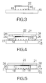
Fig. 3 is a side view of the substrate for illustrating a bonding material of solid state placed on a LSI chip; -
Fig. 4 is a side view of the substrate for illustrating thermosetting adhesives of solid state and a stiffener placed on the substrate; and -
Fig. 5 is a side view of the substrate for illustrating the thermosetting adhesives when the thermosetting adhesives melt. - Description will be made below on one embodiment of the present invention referring to the accompanying drawings.
-
Fig. 1 schematically illustrates the structure of a printedcircuit board unit 11. The printedcircuit board unit 11 includes a printedwiring board 12 made of a resin material. An electronic component package, namely an LSI (Large-Scale Integrated circuit)package 13 is mounted on the surface of the printedwiring board 12. Terminal bumps 14 are utilized to fix theLSI package 13 to the printedwiring board 12. The terminal bumps 14 may be made of an electrically-conductive material such as solder, for example. - The
LSI package 13 includes asubstrate 15 mounted on the front or upper surface of the printedwiring board 12. Thesubstrate 15 may be made of a resin material, for example. An electronic component orLSI chip 16 is mounted on the front or upper surface of thesubstrate 15. Terminal bumps 17 are utilized to fix theLSI chip 16 to thesubstrate 15. The terminal bumps 17 may be made of an electrically-conductive material such as solder, for example. The terminal bumps 17 are sealed on thesubstrate 15. Anunderfill material 18 is filled in a space between theLSI chip 16 and thesubstrate 15. A ceramic substrate may be employed as thesubstrate 15, for example. - The
LSI package 13 includes a heat conductive member orheat spreader 21. Theheat spreader 21 is received on the upward flat surface of theLSI chip 16. Theheat spreader 21 may be formed in the shape of a flat plate extending outward from the outer periphery of the upward flat surface of theLSI chip 16. Theheat spreader 21 thus completely covers over the upward flat surface of theLSI chip 16. Theheat spreader 21 may be made of a heat conductive material such as copper, aluminum, aluminum carbide, silicon carbide, aluminum silicon carbide (AlSiC) , or the like. - A
bonding material 22 having heat conductivity is interposed between theLSI chip 16 and theheat spreader 21. Thebonding material 22 extends by a constant thickness on the upward flat surface of theLSI chip 16. Thebonding material 22 serves to couple theheat spreader 21 to the upward flat surface of theLSI chip 16. A low temperature solder is employed as thebonding material 22, for example. Solidification of thebonding material 22, once melted, allows thebonding material 22 to closely contact with the upward flat surface of theLSI chip 16 without any gap. Likewise, solidification of thebonding material 22, once melted, allows thebonding material 22 to closely contact with the downward flat surface of theheat spreader 21 without any gap. - A heat radiating member or
heat sink 23 is received on theheat spreader 21. Theheat sink 23 includes a main body in the shape of a flat plate, namely aheat receiver 23a, andfins 23b standing upright in the perpendicular direction from theheat receiver 23a. Theheat receiver 23a has a downward flat surface opposed to the upward flat surface of theheat spreader 21. Parallel air passages are defined between adjacent ones of thefins 23b. Theheat sink 23 may be made of a metallic material such as aluminum, copper, or the like. Amoldingprocess may be employed to make theheat sink 23. - A fluid having heat conductivity, namely a
thermal grease 24, is interposed between the upward flat surface of theheat spreader 21 and the downward flat surface of theheat sink 23. Thethermal grease 24 includes a silicone grease and fine particles having heat conductivity, namely heat conductive filler, dispersed in the silicone grease, for example. Ceramic particles or metallic particles may be employed as the heat conductive filler, for example. Alternatively, a heat conductive sheet or a heat conductive gel may be interposed between the upward flat surface of theheat spreader 21 and the downward flat surface of theheat sink 23. - The
LSI chip 16 generates heat during its operation. The heat of theLSI chip 16 is transferred to theheat spreader 21 through thebonding material 22. The heat of theLSI chip 16 is allowed to spread over a wide range in theheat spreader 21. The heat is then transferred to theheat sink 23 through thethermal grease 24. The heat is radiated into the air from the surface of theheat sink 23 having a large surface area. Rise in the temperature of theLSI chip 16 is in this manner efficiently suppressed. In addition, the thickness of thebonding material 22 is set at the minimum permissible thickness as described later. The heat is thus efficiently transferred to theheat spreader 21 from theLSI chip 16. As long as thebonding material 22 is allowed to have the minimum permissible thickness, theLSI chip 16 is reliably prevented from an unintentional detachment from theheat spreader 21. - A support member or
stiffener 26 is fixed on thesubstrate 15 at a position adjacent to theLSI chip 16. Athermosetting adhesive 27 is interposed between thestiffener 26 and thesubstrate 15. Thethermosetting adhesive 27 serves to fix thestiffener 26 to the upward surface of thesubstrate 15. The coefficient of thermal expansion of thestiffener 21 may be set to coincide with that of thesubstrate 15, for example. In this case, thestiffener 26 may be made of copper or stainless steel, for example. Thestiffener 26 contributes to enhancement of the rigidity of thesubstrate 15. -
Athermosetting adhesive 28 is likewise interposed between thestiffener 26 and theheat spreader 21. Thethermosetting adhesive 28 serves to fix theheat spreader 21 to thestiffener 26. The weight of theheat sink 23 is thus supported on thestiffener 26. TheLSI chip 16 is allowed to only suffer from a reduced load applied through theheat sink 23. TheLSI chip 16 is in this manner prevented from suffering from destruction. The curing temperature of thethermosetting adhesives bonding material 22 as described later. The melting point of thethermosetting adhesives thermosetting adhesives bonding material 22 is preferably set sufficiently higher than the normal temperature (the room temperature, for example). The melting point of the terminal bumps 14, 17 is preferably set higher than the melting point of thebonding material 22. - As is apparent from
Fig. 2 , thestiffener 26 surrounds theLSI chip 16 without interruption on thesubstrate 15. Thestiffener 26 is interposed between theheat spreader 21 and thesubstrate 15 endlessly around theLSI chip 16. Thethermosetting adhesives stiffener 26 and thesubstrate 15 over the entire length of thestiffener 26. - Next, a detailed description will be made on a method of making the
LSI package 13. As shown inFig. 3 , for example, thesubstrate 15 is prepared. TheLSI chip 16 is mounted on thesubstrate 15. Thebonding material 22 of solid state is placed on the upward flat surface of theLSI chip 16. A low temperature solder plate having a predetermined thickness may be employed as thebonding material 22 of solid state. The contour of the low temperature solder plate may be formed to correspond to the contour of the upward flat surface of theLSI chip 16. - As shown in
Fig. 4 , thethermosetting adhesive 27 of solid state, thestiffener 26 and the thermosetting adhesive ofsolid state 28 are superposed on thesubstrate 15 in this sequence to surround theLSI chip 16. A thermosetting adhesive sheet may be employed as thethermosetting adhesives thermosetting adhesive 28 is positioned higher than the upper surface of thebonding material 22. It should be noted that the top surface of the thermosetting adhesive 28 may be positioned within a plane including the upward surface of thebonding material 22. Theheat spreader 21 is thereafter placed on the top surface of the upperthermosetting adhesive 28. Thethermosetting adhesive 27 of solid state, thestiffener 26 and thethermosetting adhesive 28 of solid state are interposed between theheat spreader 21 and thesubstrate 15. The downward surface of theheat spreader 21 is opposed to the upward surface of thebonding material 22 at a predetermined distance. - The
substrate 15 is then set in an oven. The temperature in the oven is set at a first temperature equal to or higher than the curing temperature of thethermosetting adhesives bonding material 22. Since the melting point of thethermosetting adhesives thermosetting adhesives thermosetting adhesives thermosetting adhesives thermosetting adhesives thermosetting adhesives substrate 15 and thestiffener 26 as well as between thestiffener 26 and theheat spreader 21. As shown inFig. 5 , when thethermosetting adhesives heat spreader 21 moves downward to get closer to thesubstrate 15. The downward surface of theheat spreader 21 is received on the upward surface of thebonding material 22. The weight of theheat spreader 21 is supported on thebonding material 22, theLSI chip 16, the terminal bumps 17 and theunderfill material 18. The height of theheat spreader 21 is then maintained. The aforementioned thickness of thebonding material 22 is maintained. - The first temperature is maintained in the oven for a predetermined duration. When the predetermined duration has elapsed, the
thermosetting adhesives bonding material 22 is reliably prevented from melting during the elapse of the predetermined duration. The predetermined duration is set in a range between one or two hours approximately. It should be noted that the predetermined duration depends on the property of thethermosetting adhesives - When the
thermosetting adhesives bonding material 22. Thebonding material 22 thus melts. Since thebonding material 22 of fluid state is allowed to have a predetermined viscosity and/or surface tension, thebonding material 22 of fluid state keeps filling a space between theheat spreader 21 and theLSI chip 16. The weight of theheat spreader 21 is supported on the curedthermosetting adhesives stiffener 26. Theheat spreader 21 is thus reliably prevented from a downward movement. The height of theheat spreader 21 is maintained regardless of the melting of the bodingmaterial 22. - The
substrate 15 is then taken out of the oven. Thebonding material 22 is subjected to a cooling process. Thebonding material 22 is thus hardened or cured. The height of theheat spreader 21 is maintained until thebonding material 22 is cured as described above. Thebonding material 22 is thus allowed to keep the original thickness even after thebonding material 22 has cured. The thickness of the curedbonding material 22 reliably reflects the original thickness of thebonding material 22 of solid state. When thebonding material 22 of solid state has a permissible minimum thickness, the curedbonding material 22 is allowed to keep the permissible minimum thickness. In the case where the thickness of thebonding material 22 is smaller than the permissible minimum thickness, the downward surface of theheat spreader 21 tends to suffer from an unintentional detachment from the upward flat surface of theLSI chip 16. - The method of making the
LSI package 13 allows utilization of a thermosetting adhesive of fluid state, in place of the thermosetting adhesive of solid state, interposed between thesubstrate 15 and thestiffener 26 as well as between thestiffener 26 and theheat spreader 21. In this case, the downward surface of theheat spreader 21 may be received on the upward surface of thebonding material 22 beforehand.
Claims (10)
- A method of making an electronic component, comprising:placing a bonding material on an electronic component;superposing a heat conductive member on a surface of the bonding material so as to interpose a thermosetting adhesive between the heat conductive member and a substrate;curing the thermosetting adhesive at a temperature lower than a melting point of the bonding material; andmelting the bonding material after the thermosetting adhesive has cured.
- The method according to claim 1, wherein the bonding material is solid.
- The method according to claim 1, wherein the thermosetting adhesive has fluidity.
- The method according to claim 1, wherein a support member is interposed between the heat conductive member and the substrate along with the thermosetting adhesive.
- The method according to claim 4, wherein the thermosetting adhesive surrounds the support member without interruption between the heat conductive member and the substrate.
- A method of making an electronic component, comprising:placing a bonding material on an electronic component;superposing a thermosetting adhesive and a heat conductive member on a substrate at a position adjacent to the electronic component so that the heat conductive member is opposed to a surface of the bonding material;applying heat to the thermosetting adhesive for melting the thermosetting adhesive;curing the thermosetting adhesive at a temperature lower than a melting point of the bonding material; andmelting the bonding material after the thermosetting adhesive has cured.
- A method of making a heat conductive member, comprising:placing a bonding material on a component;superposing a heat conductive member on a surface of the bonding material so as to interpose a thermosetting adhesive between the heat conductive member and a substrate;curing the thermosetting adhesive at a temperature lower than a melting point of the bonding material; andmelting the bonding material after the thermosetting adhesive has cured.
- A method of making a heat conductive member, comprising:placing a bonding material on a component;superposing a thermosetting adhesive and a heat conductive member on a substrate at a position adjacent to the component so that the heat conductive member is opposed to a surface of the bonding material;applying heat to the thermosetting adhesive for melting the thermosetting adhesive;curing the thermosetting adhesive at a temperature lower than a melting point of the bonding material; andmelting the bonding material after the thermosetting adhesive has cured.
- A method of mounting a heat conductive member for an electronic component, comprising:placing a solid bonding material on an electronic component mounted on a substrate;superposing a heat conductive member on a surface of the bonding material so that a support member and a fluid thermosetting adhesive are interposed between the heat conductive member and the substrate;maintaining a temperature equal to or higher than a curing temperature of the thermosetting adhesive and lower than a melting point of the bonding material until the thermosetting adhesive has been cured; andmelting the bonding material at a temperature equal to or higher than the melting point of the bonding material after the thermosetting adhesive has cured.
- A method of mounting a heat conductive member for an electronic component, comprising:placing a solid bonding material on an electronic component mounted on a substrate;superposing a support member, a solid thermosetting adhesive and a heat conductive member on the substrate at a position adjacent to the electronic component so that the heat conductive member is opposed to a surface of the bonding material;applying heat to the solid thermosetting adhesive so that the thermosetting adhesive melts to provide a fluid thermosetting adhesive;maintaining a temperature equal to or higher than a curing temperature of the fluid thermosetting adhesive and lower than a melting point of the bonding material until the fluid thermosetting adhesive has been cured; andmelting the bonding material at a temperature equal to or higher than the melting point of the bonding material after the fluid thermosetting adhesive has cured.
Applications Claiming Priority (1)
| Application Number | Priority Date | Filing Date | Title |
|---|---|---|---|
| PCT/JP2005/022551 WO2007066401A1 (en) | 2005-12-08 | 2005-12-08 | Process for producing electronic part, process for producing heat conducting member, and method of mounting heat conducting member for electronic part |
Publications (3)
| Publication Number | Publication Date |
|---|---|
| EP1959493A1 true EP1959493A1 (en) | 2008-08-20 |
| EP1959493A4 EP1959493A4 (en) | 2010-03-10 |
| EP1959493B1 EP1959493B1 (en) | 2012-02-08 |
Family
ID=38122554
Family Applications (1)
| Application Number | Title | Priority Date | Filing Date |
|---|---|---|---|
| EP05814186A Expired - Lifetime EP1959493B1 (en) | 2005-12-08 | 2005-12-08 | Process for producing electronic part, process for producing heat conducting member, and method of mounting heat conducting member for electronic part |
Country Status (6)
| Country | Link |
|---|---|
| US (1) | US8709197B2 (en) |
| EP (1) | EP1959493B1 (en) |
| JP (1) | JP4757880B2 (en) |
| KR (1) | KR100962100B1 (en) |
| CN (1) | CN100593238C (en) |
| WO (1) | WO2007066401A1 (en) |
Cited By (1)
| Publication number | Priority date | Publication date | Assignee | Title |
|---|---|---|---|---|
| WO2020144017A1 (en) * | 2019-01-07 | 2020-07-16 | Zf Friedrichshafen Ag | Electronic device and method for assembling an electronic device |
Families Citing this family (5)
| Publication number | Priority date | Publication date | Assignee | Title |
|---|---|---|---|---|
| KR101690820B1 (en) * | 2009-09-09 | 2016-12-28 | 미쓰비시 마테리알 가부시키가이샤 | Method for producing substrate for power module with heat sink, substrate for power module with heat sink, and power module |
| US20120188721A1 (en) * | 2011-01-21 | 2012-07-26 | Nxp B.V. | Non-metal stiffener ring for fcbga |
| US8823164B2 (en) * | 2011-10-28 | 2014-09-02 | International Business Machines Corporation | Heatsink attachment module |
| JP6512231B2 (en) * | 2017-01-27 | 2019-05-15 | トヨタ自動車株式会社 | Semiconductor device |
| CN107993995B (en) * | 2017-11-30 | 2024-01-30 | 成都信息工程大学 | A chip cooling device |
Family Cites Families (17)
| Publication number | Priority date | Publication date | Assignee | Title |
|---|---|---|---|---|
| JPS54108723A (en) | 1978-02-13 | 1979-08-25 | Kouji Isono | Enterprize condition document for management analysis |
| JPS54108273A (en) | 1978-02-14 | 1979-08-24 | Matsushita Electric Industrial Co Ltd | Method of mounting components on circuit board |
| JP2984068B2 (en) * | 1991-01-31 | 1999-11-29 | 株式会社日立製作所 | Method for manufacturing semiconductor device |
| US5219794A (en) * | 1991-03-14 | 1993-06-15 | Hitachi, Ltd. | Semiconductor integrated circuit device and method of fabricating same |
| US6021046A (en) * | 1993-06-09 | 2000-02-01 | Dallas Semiconductor Corporation | Thermal protection of electrical elements systems |
| JPH0878837A (en) | 1994-09-06 | 1996-03-22 | Matsushita Electric Ind Co Ltd | Mounting soldering method and printed circuit board with mounting solder |
| US5641713A (en) * | 1995-03-23 | 1997-06-24 | Texas Instruments Incorporated | Process for forming a room temperature seal between a base cavity and a lid using an organic sealant and a metal seal ring |
| JPH0917827A (en) * | 1995-06-29 | 1997-01-17 | Fujitsu Ltd | Semiconductor device |
| JP3219043B2 (en) | 1998-01-07 | 2001-10-15 | 日本電気株式会社 | Semiconductor device packaging method and semiconductor device |
| US6451422B1 (en) * | 1999-12-01 | 2002-09-17 | Johnson Matthey, Inc. | Thermal interface materials |
| JP2002190560A (en) | 2000-12-21 | 2002-07-05 | Nec Corp | Semiconductor device |
| KR100446290B1 (en) * | 2001-11-03 | 2004-09-01 | 삼성전자주식회사 | Semiconductor package having dam and fabricating method the same |
| JP4022758B2 (en) * | 2003-03-31 | 2007-12-19 | 株式会社デンソー | Semiconductor device |
| WO2004105129A1 (en) * | 2003-05-23 | 2004-12-02 | Fujitsu Limited | Printed circuit board unit and method of manufacturing the unit |
| US6870258B1 (en) * | 2003-06-16 | 2005-03-22 | Advanced Micro Devices | Fixture suitable for use in coupling a lid to a substrate and method |
| US7408787B2 (en) * | 2003-07-30 | 2008-08-05 | Intel Corporation | Phase change thermal interface materials including polyester resin |
| JP2006049572A (en) * | 2004-08-04 | 2006-02-16 | Toyota Motor Corp | Semiconductor device and manufacturing method thereof |
-
2005
- 2005-12-08 KR KR1020087014131A patent/KR100962100B1/en not_active Expired - Fee Related
- 2005-12-08 WO PCT/JP2005/022551 patent/WO2007066401A1/en not_active Ceased
- 2005-12-08 CN CN200580052267A patent/CN100593238C/en not_active Expired - Fee Related
- 2005-12-08 JP JP2007549001A patent/JP4757880B2/en not_active Expired - Fee Related
- 2005-12-08 EP EP05814186A patent/EP1959493B1/en not_active Expired - Lifetime
-
2008
- 2008-06-06 US US12/155,680 patent/US8709197B2/en not_active Expired - Fee Related
Cited By (1)
| Publication number | Priority date | Publication date | Assignee | Title |
|---|---|---|---|---|
| WO2020144017A1 (en) * | 2019-01-07 | 2020-07-16 | Zf Friedrichshafen Ag | Electronic device and method for assembling an electronic device |
Also Published As
| Publication number | Publication date |
|---|---|
| EP1959493B1 (en) | 2012-02-08 |
| CN100593238C (en) | 2010-03-03 |
| JP4757880B2 (en) | 2011-08-24 |
| KR100962100B1 (en) | 2010-06-09 |
| US20080295957A1 (en) | 2008-12-04 |
| US8709197B2 (en) | 2014-04-29 |
| EP1959493A4 (en) | 2010-03-10 |
| WO2007066401A1 (en) | 2007-06-14 |
| CN101326637A (en) | 2008-12-17 |
| JPWO2007066401A1 (en) | 2009-05-14 |
| KR20080073743A (en) | 2008-08-11 |
Similar Documents
| Publication | Publication Date | Title |
|---|---|---|
| US7834442B2 (en) | Electronic package method and structure with cure-melt hierarchy | |
| CN105405815B (en) | Semiconductor device and its manufacturing method | |
| TWI703681B (en) | Power overlay structure and method of making same | |
| EP2779231B1 (en) | Power overlay structure and method of making same | |
| US5811317A (en) | Process for reflow bonding a semiconductor die to a substrate and the product produced by the product | |
| US20030011997A1 (en) | Electronic assembly with solderable heat sink and methods of manufacture | |
| CN113454774A (en) | Packaged chip and manufacturing method thereof | |
| US20120098118A1 (en) | Compliant heat spreader for flip chip packaging | |
| CN102110660A (en) | Semiconductor flip chip package and method for forming semiconductor flip chip package | |
| US9721866B2 (en) | Semiconductor device having multiple bonded heat sinks | |
| US20230037617A1 (en) | Packaging structure, electronic device, and chip packaging method | |
| US8709197B2 (en) | Method of making electronic component and heat conductive member and method of mounting heat conductive member for electronic component | |
| JP4910439B2 (en) | Semiconductor device | |
| JPH11312769A (en) | Heat sink assembly for device heat dissipation | |
| US8867227B2 (en) | Electronic component | |
| CN112823416B (en) | Surface Mount Thermal Buffer | |
| JP2007066960A (en) | Semiconductor package, circuit board, and semiconductor package manufacturing method | |
| US20060273467A1 (en) | Flip chip package and method of conducting heat therefrom | |
| JP5239736B2 (en) | Electronic equipment | |
| CN221102064U (en) | Packaging structure | |
| JP2021158304A (en) | Semiconductor device and manufacturing method thereof | |
| JPH0917827A (en) | Semiconductor device | |
| JP5958136B2 (en) | Semiconductor device and manufacturing method of semiconductor device | |
| JP2003332500A (en) | Electronic circuit device | |
| KR20080052411A (en) | Semiconductor device, manufacturing method thereof, and mounting structure of semiconductor device |
Legal Events
| Date | Code | Title | Description |
|---|---|---|---|
| PUAI | Public reference made under article 153(3) epc to a published international application that has entered the european phase |
Free format text: ORIGINAL CODE: 0009012 |
|
| 17P | Request for examination filed |
Effective date: 20080702 |
|
| AK | Designated contracting states |
Kind code of ref document: A1 Designated state(s): DE FR GB |
|
| RBV | Designated contracting states (corrected) |
Designated state(s): DE FR GB |
|
| A4 | Supplementary search report drawn up and despatched |
Effective date: 20100204 |
|
| GRAP | Despatch of communication of intention to grant a patent |
Free format text: ORIGINAL CODE: EPIDOSNIGR1 |
|
| GRAS | Grant fee paid |
Free format text: ORIGINAL CODE: EPIDOSNIGR3 |
|
| GRAA | (expected) grant |
Free format text: ORIGINAL CODE: 0009210 |
|
| DAX | Request for extension of the european patent (deleted) | ||
| AK | Designated contracting states |
Kind code of ref document: B1 Designated state(s): DE FR GB |
|
| REG | Reference to a national code |
Ref country code: GB Ref legal event code: FG4D |
|
| REG | Reference to a national code |
Ref country code: DE Ref legal event code: R096 Ref document number: 602005032611 Country of ref document: DE Effective date: 20120405 |
|
| PLBE | No opposition filed within time limit |
Free format text: ORIGINAL CODE: 0009261 |
|
| STAA | Information on the status of an ep patent application or granted ep patent |
Free format text: STATUS: NO OPPOSITION FILED WITHIN TIME LIMIT |
|
| 26N | No opposition filed |
Effective date: 20121109 |
|
| REG | Reference to a national code |
Ref country code: DE Ref legal event code: R097 Ref document number: 602005032611 Country of ref document: DE Effective date: 20121109 |
|
| REG | Reference to a national code |
Ref country code: FR Ref legal event code: PLFP Year of fee payment: 11 |
|
| PGFP | Annual fee paid to national office [announced via postgrant information from national office to epo] |
Ref country code: GB Payment date: 20151202 Year of fee payment: 11 Ref country code: DE Payment date: 20151201 Year of fee payment: 11 |
|
| PGFP | Annual fee paid to national office [announced via postgrant information from national office to epo] |
Ref country code: FR Payment date: 20151110 Year of fee payment: 11 |
|
| REG | Reference to a national code |
Ref country code: DE Ref legal event code: R119 Ref document number: 602005032611 Country of ref document: DE |
|
| GBPC | Gb: european patent ceased through non-payment of renewal fee |
Effective date: 20161208 |
|
| REG | Reference to a national code |
Ref country code: FR Ref legal event code: ST Effective date: 20170831 |
|
| PG25 | Lapsed in a contracting state [announced via postgrant information from national office to epo] |
Ref country code: FR Free format text: LAPSE BECAUSE OF NON-PAYMENT OF DUE FEES Effective date: 20170102 |
|
| PG25 | Lapsed in a contracting state [announced via postgrant information from national office to epo] |
Ref country code: GB Free format text: LAPSE BECAUSE OF NON-PAYMENT OF DUE FEES Effective date: 20161208 Ref country code: DE Free format text: LAPSE BECAUSE OF NON-PAYMENT OF DUE FEES Effective date: 20170701 |