EP1956480B1 - Clock signal generation circuit and semiconductor device - Google Patents
Clock signal generation circuit and semiconductor device Download PDFInfo
- Publication number
- EP1956480B1 EP1956480B1 EP08001426A EP08001426A EP1956480B1 EP 1956480 B1 EP1956480 B1 EP 1956480B1 EP 08001426 A EP08001426 A EP 08001426A EP 08001426 A EP08001426 A EP 08001426A EP 1956480 B1 EP1956480 B1 EP 1956480B1
- Authority
- EP
- European Patent Office
- Prior art keywords
- circuit
- clock signal
- reference clock
- reset signal
- film
- Prior art date
- Legal status (The legal status is an assumption and is not a legal conclusion. Google has not performed a legal analysis and makes no representation as to the accuracy of the status listed.)
- Not-in-force
Links
Images


Classifications
-
- G—PHYSICS
- G11—INFORMATION STORAGE
- G11C—STATIC STORES
- G11C7/00—Arrangements for writing information into, or reading information out from, a digital store
- G11C7/22—Read-write [R-W] timing or clocking circuits; Read-write [R-W] control signal generators or management
-
- G—PHYSICS
- G06—COMPUTING OR CALCULATING; COUNTING
- G06F—ELECTRIC DIGITAL DATA PROCESSING
- G06F7/00—Methods or arrangements for processing data by operating upon the order or content of the data handled
- G06F7/60—Methods or arrangements for performing computations using a digital non-denominational number representation, i.e. number representation without radix; Computing devices using combinations of denominational and non-denominational quantity representations, e.g. using difunction pulse trains, STEELE computers, phase computers
- G06F7/68—Methods or arrangements for performing computations using a digital non-denominational number representation, i.e. number representation without radix; Computing devices using combinations of denominational and non-denominational quantity representations, e.g. using difunction pulse trains, STEELE computers, phase computers using pulse rate multipliers or dividers pulse rate multipliers or dividers per se
-
- G—PHYSICS
- G06—COMPUTING OR CALCULATING; COUNTING
- G06F—ELECTRIC DIGITAL DATA PROCESSING
- G06F1/00—Details not covered by groups G06F3/00 - G06F13/00 and G06F21/00
- G06F1/02—Digital function generators
- G06F1/025—Digital function generators for functions having two-valued amplitude, e.g. Walsh functions
-
- G—PHYSICS
- G06—COMPUTING OR CALCULATING; COUNTING
- G06F—ELECTRIC DIGITAL DATA PROCESSING
- G06F1/00—Details not covered by groups G06F3/00 - G06F13/00 and G06F21/00
- G06F1/04—Generating or distributing clock signals or signals derived directly therefrom
-
- G—PHYSICS
- G11—INFORMATION STORAGE
- G11C—STATIC STORES
- G11C7/00—Arrangements for writing information into, or reading information out from, a digital store
- G11C7/10—Input/output [I/O] data interface arrangements, e.g. I/O data control circuits, I/O data buffers
-
- G—PHYSICS
- G11—INFORMATION STORAGE
- G11C—STATIC STORES
- G11C7/00—Arrangements for writing information into, or reading information out from, a digital store
- G11C7/20—Memory cell initialisation circuits, e.g. when powering up or down, memory clear, latent image memory
-
- H—ELECTRICITY
- H04—ELECTRIC COMMUNICATION TECHNIQUE
- H04L—TRANSMISSION OF DIGITAL INFORMATION, e.g. TELEGRAPHIC COMMUNICATION
- H04L7/00—Arrangements for synchronising receiver with transmitter
- H04L7/02—Speed or phase control by the received code signals, the signals containing no special synchronisation information
- H04L7/033—Speed or phase control by the received code signals, the signals containing no special synchronisation information using the transitions of the received signal to control the phase of the synchronising-signal-generating means, e.g. using a phase-locked loop
Definitions
- the present invention relates to a circuit that generates a clock signal.
- the present invention relates to a semiconductor device provided with a circuit that generates such a clock signal.
- the semiconductor device can transmit and receive data without contact, for example, it can write data or read data, by transmission and reception of a communication signal by use of a wireless communication device (which can communicate wirelessly, for example, a reader/writer, a cellular phone, a personal computer, or the like).
- a wireless communication device which can communicate wirelessly, for example, a reader/writer, a cellular phone, a personal computer, or the like.
- EP 0 590 607 A1 describes a clock generation circuit comprising a first and second counter circuit, a reset signal generation circuit, a oscillator for generating a reference clock signal, and a divider circuit configured to generate an output clock signal by dividing the frequency of the reference clock signal by a division ratio, wherein the second reference clock signal has a higher frequency than the output clock signal.
- RFID technology is one of the central technologies of the ubiquitous computing era.
- RFID tags which form the basis of RFID technology have the following problems: for example, physical flexibility, high secrecy, and economical efficiency.
- an HF wireless communication CPU semiconductor device which is formed over a flexible substrate or a glass substrate and uses a wireless signal of an HF band (13.56 MHz), and the like (see Reference 1: H. Dembo et al. "RFCPUs on Glass and Plastic Substrates Fabricated by TFT Transfer Technology," IEDM Tech. Dig. Papers, pp. 1067-1069, 2005 ).
- a semiconductor device which transmits and receives data by a wireless signal requires very high performance, such as extension of communication distance, low power consumption, miniaturization of chips, and high reliability of encoding communication.
- a wireless signal of a UHF band (915 MHz) can be used. Because the wireless signal of a UHF band can be used to perform long-distance communication in principle, compared with a wireless signal of an HF band, the wireless signal of a UHF band has an advantageous effect for extension of communication distance.
- a communication signal of a UHF band there are many problems in circuit design, such as generation of a stable clock signal in the semiconductor device; therefore, it is necessary to dramatically review the design of an HF wireless communication CPU.
- a PLL circuit As for a clock signal generation circuit used to generate a clock signal, a PLL circuit is generally used in many cases.
- the PLL circuit is formed of a voltage control oscillator circuit (VCO), a loop filter circuit, a phase comparator, a divider circuit, and the like.
- VCO voltage control oscillator circuit
- a PLL circuit is mounted on a semiconductor device which transmits and receives data by a wireless signal, it is difficult to obtain a stable clock signal. For example, during a free-running period after a synchronous period is terminated, there is a case where a power supply voltage in the VCO changes in some cases. In addition, there is a case where a frequency of a clock signal does not reach a stable value during the synchronous period.
- an object of the present invention is to provide a semiconductor device which operates stably at low cost by providing a clock signal generation circuit that can supply a stable clock signal.
- the present invention provides a clock signal generation circuit comprising:
- a clock signal generation circuit which can generate a stable clock signal and which operates stably and a semiconductor device provided with the clock signal generation circuit can be provided at low cost.
- a clock signal generation circuit of the present invention will be described.
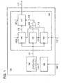
- a clock signal generation circuit (also referred to as a clock generator) 100 includes a constant voltage circuit (also referred to as a regulator) 101, a reference clock signal generation circuit 102, and a counter group 103.
- the counter group 103 includes a first counter circuit 104, a second counter circuit 105, a first divider circuit 106, a second divider circuit 107, and a reset signal generation circuit 108.
- the constant voltage circuit 101 is connected to the reference clock signal generation circuit 102.
- the reference clock signal generation circuit 102 is connected to the first counter circuit 104, the second counter circuit 105, and the first divider circuit 106.
- the first counter circuit 104 is connected to the second counter circuit 105, the first divider circuit 106, and the reset signal generation circuit 108.
- the second counter circuit 105 is connected to the reset signal generation circuit 108.
- the first divider circuit 106 is connected to the second divider circuit 107.
- the constant voltage circuit 101 generates a second power supply voltage ( VDD RO ) 110 having a constant voltage value from a first power supply voltage (VDD CG ) 109 and has a function used to supply the second power supply voltage (VDD RO ) 110 to the reference clock signal generation circuit 102.
- the reference clock signal generation circuit 102 has a function used to generate a first reference clock signal ( CLK RO ) 111 having a frequency f RO by use of the second power supply voltage 110.
- CLK RO first reference clock signal
- As the reference clock signal generation circuit 102 for example, a ring oscillator, a crystal oscillator, or the like can be used. Note that in the following description, frequencies of the first reference clock signal 111 in a synchronous (SYNC) period and an asynchronous (ASYNC) period are denoted by f ROS and f RONS , respectively.
- the first counter circuit 104 generates a first reset signal ( RST MASTER ) 113 by use of a synchronizing signal (SYNC) 112 to be effective in a period To in a synchronous period and also counts the number of rising edges of the first reference clock signal 111 using the first reset signal 113 as a reset signal.
- RST MASTER a first reset signal
- SYNC synchronizing signal
- a "signal that is to be effective” (also referred to as “to be asserted") is synonymous with a “signal or logic in an electric circuit that is to be effective (to be active)".
- the direction of current flow, whether there is a current or not, or the like is determined by control of a voltage level, and on or off is expressed according to the direction of current flow or whether there is a current; however, since this expression method is mixed and used according to aims, it is difficult to interpret. Consequently, a signal state can be expressed regardless of a voltage level by expressing the signal state based on whether a signal is effective or non-effective.
- the first divider circuit 106 divides the frequency of the first reference clock signal 111 by use of the first reset signal 113 as a reset signal and generates a second reference clock signal ( CLK SYS ) 115.
- the reset signal generation circuit 108 is formed of an OR circuit and has a function used to output a third reset signal 116 to the second divider circuit 107 when the reset signal is input from the first counter circuit 104 or the second counter circuit 105.
- T 0 is a value determined by communication standards.
- n T 0 and n SYS are integer values determined by design specifications.
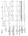
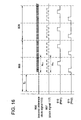
- a first signal waveform 801 corresponds to a signal waveform of the synchronizing signal 112
- a second signal waveform 802 corresponds to an enumerated value of the first counter circuit 104
- a third signal waveform 803 corresponds to an enumerated value of the second counter circuit 105
- a fourth signal waveform 804 corresponds to a signal waveform of the first reset signal 113
- a fifth signal waveform 805 corresponds to a signal waveform of the second reset signal 114
- a sixth signal waveform 806 corresponds to a signal waveform of the second reference clock signal 115
- a seventh signal waveform 807 corresponds to a signal waveform of the clock signal 117.
- a synchronous period (SYNC period) 808 the synchronizing signal 112 is to be effective in each period To, as shown by the first signal waveform 801; therefore, in the first counter circuit 104, the first reset signal 113, like the fourth signal waveform 804, is generated by use of the synchronizing signal 112.
- the synchronizing signal 112 is input to a flip-flop circuit which is operated using the first reference clock signal 111 so that a signal which is synchronized with the first reference clock signal 111 is generated.
- the first counter circuit 104 counts the number of rising edges of the first reference clock signal 111 using the first reset signal 113 as a reset signal. Enumerated values (count values) correspond to form a pattern like the second signal waveform 802. Note that counting is continued until the next time that the synchronizing signal 112 is effective, and an enumerated value n T 0 at this point is supplied to the second counter circuit 105 and the first divider circuit 106.
- an asynchronous period (ASYNC period) 809 because the synchronizing signal 112 is in an ineffective state, the first counter circuit 104 continues counting. In addition, since the first reset signal 113 is not generated, the enumerated value n T 0 is not updated.
- the second counter circuit 105 determines whether the enumerated value n T 0 which has been counted by the first counter circuit 104 is a normal value or not, and in the case where it is determined to be a normal value, counting of rising edges of the first reference clock signal 111 is started.
- counting is performed up to the enumerated value n T 0 which has been counted by the first counter circuit 104 in a period To just before the period when counting is performed by the second counter circuit 105 is to start; whenever counting is performed up to a value of n T 0 , the second reset signal 114 that looks like the fifth signal waveform 805 is generated, an enumerated value is reset, and counting is resumed. That is, a counter value of the second counter circuit 105 is set to look like the third signal waveform 803.
- determination of whether the enumerated value n T 0 has a normal value or not refers to whether an enumerated value, for example, the enumerated value n T 0 , is normal is determined by whether the enumerated value lies within the range which is decided in advance by a specification. In addition, determination is performed at the time when the enumerated value n T 0 is updated.
- INT is a function used to denote only an integer which is calculated in such a way that a value of n T 0 divided by n SYS is truncated at the decimal point.
- n SYS which is a design parameter is desirably set as the n-th (n is a natural number) power of two.
- n SYS is set as the n-th power of two
- a high-order bit other than a low n bit of the enumerated value n T 0 can be set as a division ratio.
- the chip area of the clock signal generation circuit 100 can be reduced. Note that the signal waveform of the second reference clock signal 115 corresponds to the sixth signal waveform 806.
- determination of whether the enumerated value n T 0 has a normal value or not refers to whether an enumerated value, for example, the enumerated value n T0 , is normal is determined by whether the enumerated value lies within the range which is decided in advance by a specification. In addition, determination is performed at the time when the enumerated value n T 0 is updated.
- the reset signal generation circuit 108 outputs an input reset signal as the third reset signal 116 to the second divider circuit 107 when the first reset signal generated in the first counter circuit or the second reset signal generated in the second counter circuit is input.
- the second divider circuit 107 divides the frequency of the second reference clock signal 115 by using the third reset signal 116 as a reset signal and generates n PH pulses until the next period in which the third reset signal 116 is effective.
- n PH is a design parameter.
- the third reset signal 116 is effective, the frequency of the second reference clock signal 115 begins to be divided by a division ratio set in advance to generate the clock signal 117.
- the number of pulses of the clock signal 117 is counted, and when the number of pulses reaches n PH, generation of the clock signal 117 is stopped.
- the next time that the third reset signal 116 is effective generation of the clock signal 117 is resumed.
- the signal waveform of the clock signal 117 corresponds to the seventh signal waveform 807.
- a dividing operation in the second divider circuit 107 starts frequency dividing by using the first reset signal 113 as the third reset signal 116, as shown by the second reference clock signal 115 of the signal waveform 806 and the clock signal 117 of the signal waveform 807 in FIG. 8 ; however, in the case where the second reset signal 114 is set as the third reset signal 116, frequency dividing is started by using the second reset signal 114 as the third reset signal 116.
- each of the first counter circuit 104, the second counter circuit 105, the first divider circuit 106, and the second divider circuit 107 is formed of a flip-flop circuit and at least one of a latch circuit, a NOT circuit, an AND circuit, an OR circuit, a NAND circuit, and a NOR circuit so that each operation of counting or frequency dividing can be performed in the clock signal generation circuit 100.
- a signal having n PH pulses can be generated in each period To. That is, the clock signal 117 which has an average frequency of 1/ n PH T 0 can be generated.
- frequency accuracy is caused by an error introduced into the equation due to the quantization of To, namely, a quantization error which is a "remainder" term by counting To by use of the counted number of rising edges n T 0 of the first reference clock signal 111.
- the quantization error is proportional to the inverse of n T0 . Accordingly, by increasing n T 0 , namely, by increasing the frequency of the first reference clock signal 111, the quantization error can be reduced comparatively. That is, it is found that frequency accuracy can be easily increased.
- frequency variation is caused by a difference in frequencies of the first reference clock signal 111 in the synchronous period and the asynchronous period. Because of a relationship between To and T 0NS , a relationship where [(1-1/ n T0 ) ⁇ ( f RONS / f ROS )] ⁇ ( f PHNS / f PHS ) ⁇ [(1+1/ n T0 ) ⁇ ( f RONS / f ROS )] is obtained quantitatively. That is, by increasing the number of pulses n T 0 , namely, by increasing the frequency of the first reference clock signal 111, a change in frequency can be reduced comparatively. In the clock signal generation circuit of the present invention, when the second power supply voltage 110 which is supplied to the reference clock signal generation circuit 102 is supplied from the constant voltage circuit 101, a change in frequency of the first reference clock signal 111 can be reduced.
- the clock signal generation circuit provided with a plurality of counter circuits and a plurality of divider circuits, a clock signal with high frequency accuracy and very low frequency variation can be generated.
- a semiconductor device which can realize a stable operation even with wireless communication at the UHF band, for example, can be provided at low cost.
- a structure of the semiconductor device of this embodiment is shown in FIG 3 .
- a semiconductor device 300 includes an RF circuit 301, a clock signal generation circuit 302, a logic circuit 303, and an antenna 317 in an antenna portion 318. Note that, although not shown in FIG 3 , the semiconductor device 300 transmits and receives a wireless signal to and from an external circuit such as a wireless communication device via the antenna 317.
- the RF circuit 301 includes a power supply circuit 304, a demodulation circuit 305, and a modulation circuit 306.
- the clock signal generation circuit 302 includes a constant voltage circuit 307, a ring oscillator 308, and a counter group 309.
- the logic circuit 303 includes a controller 313, a CPU (also referred to as a central processing unit) 310, a ROM (read only memory) 311, and a RAM (random access memory) 312.
- the controller 313 includes a CPU interface 314, an RF interface 315, and a memory controller 316.
- the power supply circuit 304 is formed of a rectifier circuit and a storage capacitor and has a function used to supply a first power supply voltage to another circuit.
- the demodulation circuit 305 is formed of a rectifier circuit and an LPF (low-pass filter) and has a function used to extract a command or data from a communication signal.
- the modulation circuit 306 has a function used to modulate transmission data, and modulated data is transmitted as a transmitted signal from the antenna 317.
- the semiconductor device 300 receives a received signal which is transmitted from an external communication device.
- the received signal is demodulated by the demodulation circuit 305 and then input to the RF interface 315 in the controller 313.
- the received signal which is input to the RF interface 315 is processed arithmetically by the CPU 310 through the CPU interface 314.
- access to the ROM 311 and the RAM 312 is performed through the memory controller 316.
- Transmission data is generated after arithmetic processing is performed by the CPU 310 and data in the ROM 311 and the RAM 312 is input and output, the transmission data is modulated in the modulation circuit 306, and a transmitted signal is transmitted from the antenna 317 to the communication device.
- the clock signal generation circuit 100 of the invention shown in FIG 1 can be applied to the clock signal generation circuit 302 in this embodiment mode.
- the constant voltage circuit 101, the reference clock signal generation circuit 102, and the counter group 103 correspond to the constant voltage circuit 307, the ring oscillator 308, and the counter group 309, respectively.
- the semiconductor device provided with the clock signal generation circuit of the present invention can realize a stable operation, and a semiconductor device which can realize a stable operation even with wireless communication that uses the UHF band, for example, can be provided at low cost.
- a method for manufacturing a semiconductor device described in the above embodiment will be described.
- example 1 a structure in which a semiconductor device including an antenna circuit is provided over the same substrate will be described.
- an insulating film 1902 is formed over one surface of a substrate 1901, and a peeling layer 1903 is formed over the substrate 1901 with the insulating film 1902 interposed therebetween, and then an insulating film 1904 functioning as a base film and a semiconductor film 1905 (e.g., a film containing amorphous silicon) are formed thereover.
- a semiconductor film 1905 e.g., a film containing amorphous silicon
- the substrate used for the substrate 1901 is selected from a glass substrate, a quartz substrate, a ceramic substrate, a metal substrate (e.g., a stainless steel substrate), a semiconductor substrate such as an Si substrate, or the like.
- a plastic substrate made of polyethylene terephthalate (PET), polyethylene naphthalate (PEN), polyether sulfone (PES), acrylic, or the like can be selected.
- the peeling layer 1903 is provided over the entire surface of the substrate 1901 with the insulating film 1902 interposed therebetween, the peeling layer can also be selectively provided by a photolithography method after being provided over the entire surface of the substrate 1901.
- the insulating films 1902 and 1904 are formed using a material such as silicon oxide, silicon nitride, silicon oxynitride (SiO x N y , where x > y > 0), or silicon nitride oxide (SiN x O y , where x > y > 0) by a CVD method, a sputtering method, or the like.
- a silicon nitride oxide film may be formed as a first insulating film and a silicon oxynitride film may be formed as a second insulating film.
- a silicon nitride film may be formed as a first insulating film and a silicon oxide film may be formed as a second insulating film.
- the insulating film 1902 functions as a blocking layer which prevents an impurity element contained in the substrate 1901 from being mixed into the peeling layer 1903 or elements formed thereover.
- the insulating film 1904 functions as a blocking layer which prevents an impurity element contained in the substrate 1901 or the peeling layer 1903 from being mixed into elements formed over the insulating film 1904.
- an impurity element such as an alkali metal element such as Na or an alkaline earth metal element, contained in the substrate 1901 can be prevented from adversely affecting the element formed over the substrate 1901, and an impurity element contained in the peeling layer 1903 can be prevented from adversely affecting the element formed over the peeling layer 1903.
- the insulating films 1902 and 1904 may be omitted.
- the peeling layer 1903 may be formed using a metal film, a stacked structure of a metal film and a metal oxide film, or the like.
- a metal film either a single layer or stacked layers are formed using an element selected from tungsten, molybdenum, titanium, tantalum, niobium, nickel, cobalt, zirconium, zinc, ruthenium, rhodium, palladium, osmium, and iridium, or an alloy material or a compound material containing the element as its main component.
- such materials can be formed by a sputtering method, various CVD methods such as a plasma CVD method, or the like.
- a stacked structure of a metal film and a metal oxide film can be obtained by the steps of forming the above-described metal film and applying plasma treatment thereto under an oxygen atmosphere or an N 2 O atmosphere or applying heat treatment thereto under an oxygen atmosphere or an N 2 O atmosphere, and thereby forming oxide or oxynitride of the metal film on the metal film.
- a metal oxide film made of tungsten oxide can be formed on the surface of the tungsten film by applying plasma treatment to the tungsten film.
- the tungsten oxide can be represented by WO x where x is in the range of 2 to 3.
- tungsten oxide there are cases where x is 2 (WO 2 ), x is 2.5 (W 2 O 5 ) x is 2.75 (W 4 O 11 x is 3 (WO 3 ), and the like.
- a metal film e.g., tungsten
- an insulating film formed of silicon oxide or the like may be formed over the metal film by a sputtering method, and also metal oxide (e.g., tungsten oxide over tungsten) may be formed over the metal film.
- the above-described high-density plasma treatment may be applied as the plasma treatment, for example.
- metal nitride or metal oxynitride may also be formed.
- plasma treatment or heat treatment may be applied to the metal film under a nitrogen atmosphere or under an atmosphere containing nitrogen and oxygen.
- the semiconductor film 1905 is formed to a thickness of greater than or equal to 25 nm and less than or equal to 200 nm (preferably, greater than or equal to 30 nm and less than or equal to 150 nm) by a sputtering method, an LPCVD method, a plasma CVD method, or the like.
- the amorphous semiconductor film 1905 is crystallized by laser beam irradiation.
- the crystallization of the amorphous semiconductor film 1905 may also be conducted by a method combining the laser crystallization with a thermal crystallization method using RTA or an annealing furnace or with a thermal crystallization method using a metal element that promotes the crystallization, or the like.
- the crystallized semiconductor film is etched into desired shapes, whereby crystalline semiconductor films 1905a, 1905b, 1905c, 1905d, 1905e, and 1905f are formed.
- a gate insulating film 1906 is formed so as to cover the semiconductor films 1905a to 1905f.
- the gate insulating film 1906 is formed using a material such as silicon oxide, silicon nitride, silicon oxynitride (SiO x N y , where x > y > 0), or silicon nitride oxide (SiN x O y , where x > y > 0) by a CVD method, a sputtering method, or the like.
- a material such as silicon oxide, silicon nitride, silicon oxynitride (SiO x N y , where x > y > 0), or silicon nitride oxide (SiN x O y , where x > y > 0) by a CVD method, a sputtering method, or the like.
- a silicon oxynitride film as a first insulating film and a silicon nitride oxide film as a second insulating film.
- an amorphous semiconductor film with a thickness of greater than or equal to 50 nm and less than or equal to 60 nm is formed by a plasma CVD method.
- a solution containing nickel which is a metal element used to promote crystallization is made to be retained on the amorphous semiconductor film, which is followed by dehydrogenation treatment (at 500°C for one hour) and thermal crystallization treatment (at 550°C for four hours). In this way, a crystalline semiconductor film is formed.
- the crystalline semiconductor film is irradiated with a laser beam by a photolithography method and etched so that the crystalline semiconductor films 1905a to 1905f are formed.
- crystallization of the amorphous semiconductor film may be conducted using laser beam irradiation only, without performance of thermal crystallization which uses a metal element that promotes crystallization.
- a laser oscillator used for crystallization either a continuous wave laser (a CW laser) or a pulsed laser can be used.
- a laser that can be used here there are gas lasers such as an Ar laser, a Kr laser, and an excimer laser; a laser in which single-crystalline YAG, YVO 4 , forsterite (Mg 2 SiO 4 ), YAlO 3 , or GdVO 4 or polycrystalline (ceramic) YAG, Y 2 O 3 , YVO 4 , YAlO 3 , or GdVO 4 is doped with one or more laser media selected from among Nd, Yb, Cr, Ti, Ho, Er, Tm, and Ta as dopant; a glass laser; a ruby laser; an alexandrite laser; a Ti:sapphire laser; a copper vapor laser; and a metal vapor laser.
- crystals with a large grain size can be obtained.
- the second harmonic (532 nm) or the third harmonic (355 nm) of an Nd:YVO 4 laser (the fundamental wave of 1064 nm) can be used.
- a laser power density of about greater than or equal to 0.01 MW/cm 2 and less than or equal to 100 MW/cm 2 (preferably, greater than or equal to 0.1 MW/cm 2 and less than or equal to 10 MW/cm 2 ) is required, and irradiation is conducted with a scanning rate of about greater than or equal to 10 cm/sec and less than or equal to 2000 cm/sec.
- the gate insulating film 1906 may be formed by oxidization or nitridation of the surfaces of the semiconductor films 1905a to 1905f by the above-described high-density plasma treatment.
- plasma treatment with a mixed gas of a noble gas such as He, Ar, Kr, or Xe, and oxygen, nitrogen oxide, ammonia, nitrogen, or hydrogen is used.
- a mixed gas of a noble gas such as He, Ar, Kr, or Xe
- oxygen, nitrogen oxide, ammonia, nitrogen, or hydrogen is used.
- plasma When plasma is excited by the introduction of microwaves, plasma with a low electron temperature and a high electron density can be generated.
- oxygen radicals which may include OH radicals
- nitrogen radicals which are generated by the high-density plasma, the surfaces of the semiconductor films can be oxidized or nitrided.
- an insulating film only formed by high-density plasma treatment may be used, or a stacked layer which is obtained by depositing an insulating film formed of at least one of silicon oxide, silicon oxynitride, and silicon nitride on the insulating film by a CVD method using plasma or thermal reaction may be used. In either case, the amount of variation in characteristics of transistors which each include an insulating film formed by high-density plasma treatment as part or all of its gate insulating film can be reduced.
- the semiconductor films 1905a to 1905f which are obtained by irradiation of a semiconductor film with a continuous wave laser beam or a laser beam oscillated with a repetition rate of 10 MHz or more and scanning of the semiconductor film in one direction to crystallize the semiconductor film, have a characteristic in that their crystals grows in the beam scanning direction.
- a transistor is arranged so that its channel length direction (direction in which carriers move when a channel formation region is formed) is aligned with the scanning direction, and the above-described gate insulating film 1906 is combined with the semiconductor film, so that a thin film transistor (TFT) with high electron field-effect mobility and few variations in characteristics can be obtained.
- TFT thin film transistor
- first conductive film and a second conductive film are stacked over the gate insulating film 1906.
- the first conductive film is formed to have a thickness of greater than or equal to 20 nm and less than or equal to 100 nm by a CVD method, a sputtering method, or the like.
- the second conductive film is formed to have a thickness of greater than or equal to 100 nm and less than or equal to 400 nm.
- the first conductive film and the second conductive film are each formed of an element selected from among tantalum, tungsten, titanium, molybdenum, aluminum, copper, chromium, niobium, and the like, or an alloy material or a compound material containing the element as its main component.
- the first conductive film and the second conductive film are formed of a semiconductor material typified by polycrystalline silicon doped with an impurity element such as phosphorus.
- a tantalum nitride film and a tungsten film As examples of combinations of the first conductive film and the second conductive film, a tantalum nitride film and a tungsten film; a tungsten nitride film and a tungsten film; a molybdenum nitride film and a molybdenum film; and the like can be given.
- Tungsten and tantalum nitride have high heat resistance. Therefore, after forming the first conductive film and the second conductive film, thermal treatment can be applied thereto for the purpose of heat activation.
- gate electrodes 1907 are formed above the semiconductor films 1905a to 1905f.
- a stacked structure of a first conductive film 1907a and a second conductive film 1907b is shown as an example of the gate electrode 1907.
- the semiconductor films 1905a to 1905f are doped at a low concentration with an impurity element which imparts n-type conductivity, using the gate electrodes 1907 as masks, by an ion doping method or an ion implantation method. Then, a resist mask is selectively formed by a photolithography method, and any of the semiconductor films 1905a to 1905f are doped at high concentration with an element which imparts p-type conductivity.
- an impurity element which imparts n-type conductivity phosphorus, arsenic, or the like can be used.
- As an element which imparts p-type conductivity boron, aluminum, gallium, or the like can be used.
- phosphorus is used as an impurity element which imparts n-type conductivity and is selectively introduced into the semiconductor films 1905a to 1905f so that phosphorus is contained at concentrations of greater than or equal to 1 x 10 15 /cm 3 and less than or equal to 1 ⁇ 10 19 /cm 3 .
- n-type impurity regions 1908 are formed.
- boron is used as an element which imparts p-type conductivity and is selectively introduced into the semiconductor films 1905c and 1905e so as to be contained at concentrations of greater than or equal to 1 ⁇ 10 19 /cm 3 and less than or equal to 1 ⁇ 10 20 /cm 3 .
- p-type impurity regions 1909 are formed.
- an insulating film is formed so as to cover the gate insulating film 1906 and the gate electrodes 1907.
- the insulating film is formed to be either a single layer or a stacked layer of at least one of a film containing an inorganic material such as silicon, silicon oxide, or silicon nitride or a film containing an organic material such as an organic resin by a plasma CVD method, a sputtering method, or the like.
- the insulating film is selectively etched by anisotropic etching mainly in the perpendicular direction so that insulating films 1910 (also referred to as sidewalls) which are in contact with the side surfaces of the gate electrodes 1907 are formed.
- the insulating films 1910 are used as doping masks for forming LDD (lightly doped drain) regions.
- the semiconductor films 1905a, 1905b, 1905d, and 1905f are doped with an impurity element which imparts n-type conductivity at high concentration, using the resist mask formed by a photolithography method, the gate electrodes 1907, and the insulating films 1910 as masks.
- n-type impurity regions 1911 are formed.
- phosphorus (P) is used as an impurity element which imparts n-type conductivity, and is selectively introduced into the semiconductor films 1905a, 1905b, 1905d, and 1905f so as to be contained at concentrations of greater than or equal to 1 ⁇ 10 19 /cm 3 and less than or equal to 1 ⁇ 10 20 /cm 3 .
- the n-type impurity regions 1911 with a higher concentration of impurity than that of the impurity regions 1908 are formed.
- n-channel thin film transistors 1900a, 1900b, 1900d, and 1900f, and p-channel thin film transistors 1900c and 1900e are formed.
- n-channel thin film transistor 1900a a channel formation region is formed in a region of the semiconductor film 1905a which overlaps with the gate electrode 1907; the impurity region 1911 which forms a source or drain region is formed in a region of the semiconductor film 1905a which does not overlap with the gate electrode 1907 and the insulating film 1910; and a low concentration impurity region (LDD region) is formed in a region which overlaps with the insulating film 1910 and between the channel formation region and the impurity region 1911.
- channel formation regions, low concentration impurity regions, and the impurity regions 1911 are formed in the n-channel thin film transistors 1900b, 1900d, and 1900f.
- a channel formation region is formed in a region of the semiconductor film 1905c which overlaps with the gate electrode 1907, and the impurity region 1909 which forms a source or drain region is formed in a region which does not overlap with the gate electrode 1907.
- a channel formation region and the impurity region 1909 are formed in the p-channel thin film transistor 1900e.
- LDD regions are not formed in the p-channel thin film transistors 1900c and 1900e, LDD regions may be provided in the p-channel thin film transistors or a structure without LDD regions may be applied to the n-channel thin film transistors.
- an insulating film with a single layer or stacked layers is formed so as to cover the semiconductor films 1905a, 1905b, 1905c, 1905d, 1905e, and 1905f, the gate electrodes 1907, and the like. Then, a conductive film 1913 electrically connected to the impurity regions 1909 and 1911 which form the source and drain regions of the thin film transistors 1900a to 1900f is formed over the insulating film.
- the insulating film is formed either in a single layer or in stacked layers, using at least one of an inorganic material such as silicon oxide or silicon nitride, an organic material such as polyimide, polyamide, benzocyclobutene, acrylic, or epoxy, a siloxane material, or the like by a CVD method, a sputtering method, an SOG method, a droplet discharging method, a screen printing method, or the like.
- the insulating film is formed to have two layers such that a first insulating film 1912a is formed of a silicon nitride oxide film and a second insulating film 1912b is formed of a silicon oxynitride film.
- the conductive film 1913 can form the source and drain electrodes of the semiconductor films 1905a to 1905f.
- heat treatment is preferably applied for recovery of the crystallinity of the semiconductor films, activation of the impurity element which has been added into the semiconductor films, or hydrogenation of the semiconductor films.
- thermal annealing, laser annealing, RTA, or the like is preferably applied.
- the conductive film 1913 is formed of either a single layer or a stacked layer of an element selected from among aluminum, tungsten, titanium, tantalum, molybdenum, nickel, platinum, copper, gold, silver, manganese, neodymium, carbon, and silicon, or an alloy material or a compound material containing the element as its main component by a CVD method, a sputtering method, or the like.
- An alloy material containing aluminum as its main component corresponds to, for example, a material which contains aluminum as its main component and also contains nickel, or a material which contains aluminum as its main component and also contains nickel and one or both of carbon and silicon.
- the conductive film 1913 is preferably formed to have a stacked structure of a barrier film, an aluminum-silicon (Al-Si) film, and a barrier film or a stacked structure of a barrier film, an aluminum silicon (Al-Si) film, a titanium nitride film, and a barrier film.
- the "barrier film” corresponds to a thin film formed of titanium, titanium nitride, molybdenum, or molybdenum nitride.
- Aluminum and aluminum silicon are the most suitable material for forming the conductive film 1913 because they have low resistance value and are inexpensive. When barrier layers are provided in the top layer and the bottom layer, generation of hillocks of aluminum or aluminum silicon can be prevented.
- the natural oxide film can be chemically reduced, and a favorable contact between the conductive film 1913 and the crystalline semiconductor film can be obtained.
- an insulating film 1914 is formed so as to cover the conductive film 1913, and conductive films 1915a and 1915b electrically connected to the conductive film 1913 which forms the source electrode or the drain electrode of each of the semiconductor films 1905a and 1905f are formed over the insulating film 1914.
- conductive films 1916a and 1916b electrically connected to the conductive film 1913 which forms the source electrode or the drain electrode of each of the semiconductor films 1905b and 1905e are formed.
- the conductive films 1915a and 1915b and the conductive films 1916a and 1916b may be formed using the same material at the same time.
- the conductive films 1915a and 1915b and the conductive films 1916a and 1916b may be formed using any of the above-described materials which can be used for the conductive film 1913.
- conductve films 1917a and 1917b functioning as antennas are formed so as to be electrically connected to the conductive films 1916a and 1916b, respectively.
- the insulating film 1914 can be formed of either a single layer or a stacked structure of an insulating film containing oxygen or nitrogen such as silicon oxide (SiO x ), silicon nitride (SiN x ), silicon oxynitride (SiO x N y , where x > y > 0), or silicon nitride oxide (SiN x O y , where x > y > 0); a film containing carbon such as DLC (diamond-like carbon); an organic material such as epoxy, polyimide, polyamide, polyvinyl phenol, benzocyclobutene, or acrylic; a siloxane material containing a siloxane resin; or the like by a CVD method, a sputtering method, or the like.
- silicon oxide SiO x
- SiN x silicon nitride
- SiO x N y silicon oxynitride
- SiN x O y silicon n
- a siloxane material corresponds to a material that has a bond of Si-O-Si.
- Siloxane has a skeleton structure with a bond of silicon and oxygen.
- an organic group containing at least hydrogen e.g., an alkyl group or aromatic hydrocarbon
- a fluoro group may be used as the substituent.
- both a fluoro group and an organic group containing at least hydrogen may be used as the substituent.
- the conductive films 1917a and 1917b can be formed of a conductive material by a CVD method, a sputtering method, a printing method such as screen printing or gravure printing, a droplet discharging method, a dispensing method, a plating method, or the like.
- the conductive films 1917a and 1917b are formed of a single layer or a stacked structure of an element selected from among aluminum, titanium, silver, copper, gold, platinum, nickel, palladium, tantalum, and molybdenum or an alloy material or a compound material containing the element as its main component.
- the antenna can be provided by selective printing of a conductive paste in which conductive particles with a grain diameter of several nanometers to several tens of micrometers are dissolved or dispersed in an organic resin.
- the conductive particles can be at least one of metal particles selected from among silver, gold, copper, nickel, platinum, palladium, tantalum, molybdenum, and titanium; fine particles of silver halide; and dispersive nanoparticles.
- the organic resin included in the conductive paste can be one or more of organic resins which function as a binder, a solvent, a dispersing agent, or a coating material for the metal particles.
- an organic resin such as an epoxy resin and a silicone resin can be given as examples.
- baking is preferably performed after the conductive paste is applied.
- fine particles e.g., particles with a grain diameter of greater than or equal to 1 nm and less than or equal to 100 nm
- the conductive paste is baked and hardened at temperatures in the range of greater than or equal to 150°C and less than or equal to 300°C to obtain the conductive film.
- fine particles containing solder or lead-free solder as the main component. In that case, fine particles with a grain diameter of 20 ⁇ m or less are preferably used. Solder and lead-free solder have the advantage of being low in cost.
- an insulating film 1918 is formed so as to cover the conductive films 1917a and 1917b
- layers including the thin film transistors 1900a to 1900f, the conductive films 1917a and 1917b, and the like are separated from the substrate 1901.
- the element formation layer 1919 can be separated from the substrate 1901 using physical force.
- the peeling layer 1903 may be selectively removed by introduction of an etchant into the openings before the element formation layer 1919 is separated from the substrate 1901.
- a gas or a liquid containing halogen fluoride or a halogen compound is used as the etchant.
- chlorine trifluoride (CIF 3 ) is used as the gas containing halogen fluoride
- the element formation layer 1919 can be separated from the substrate 1901.
- the whole peeling layer 1903 is not removed but part thereof may be left behind. Accordingly, the amount of etchant used can be reduced and process time for removing the peeling layer can be shortened.
- the element formation layer 1919 can be maintained over the substrate 1901.
- cost reduction can be achieved.
- the insulating film 1918 can be formed of either a single layer or a stacked structure of an insulating film containing oxygen or nitrogen such as silicon oxide (SiO x ), silicon nitride (SiN x ), silicon oxynitride (SiO x N y , where x > y > 0), or silicon nitride oxide (SiN x O y , where x > y > 0); a film containing carbon such as DLC (diamond-like carbon); an organic material such as epoxy, polyimide, polyamide, polyvinyl phenol, benzocyclobutene, or acrylic; a siloxane material containing a siloxane resin; or the like by a CVD method, a sputtering method, or the like.
- silicon oxide SiO x
- SiN x silicon nitride
- SiO x N y silicon oxynitride
- SiN x O y silicon n
- a first sheet material 1920 is attached to one surface of the element formation layer 1919 (the surface where the insulating film 1918 is exposed), and then the element formation layer 1919 is separated from the substrate 1901.
- a second sheet material 1921 is attached to the other surface of the element formation layer 1919 (the surface exposed by peeling), followed by one or both of heat treatment and pressurization treatment.
- the first sheet material 1920 and the second sheet material 1921 hot-melt films and the like can be used.
- an antistatic film a film on which antistatic treatment for preventing static electricity or the like has been applied
- an antistatic film a film in which an antistatic material is dispersed in a resin, a film to which an antistatic material is attached, and the like
- the film provided with an antistatic material can be a film with an antistatic material provided over one of its surfaces, or a film with an antistatic material provided over each of its surfaces.
- the film with an antistatic material provided over one of its surfaces may be attached to the layer so that the antistatic material is placed on the inner side of the film or the outer side of the film.
- the antistatic material may be provided over the entire surface of the film, or over a part of the film.
- a metal, indium tin oxide (ITO), or a surfactant such as an amphoteric surfactant, a cationic surfactant, or a nonionic surfactant can be used.
- a resin material which contains a cross-linked copolymer having a carboxyl group and a quaternary ammonium base on its side chain, or the like can be used as an antistatic material. Such a material is attached, mixed, or applied to a film, so that an antistatic film can be formed. By sealing with the antistatic film, the semiconductor element can be prevented from adverse effects such as external static electricity when being dealt with as a commercial product.
- the element formation layer 1919 may be formed over the substrate 1901 and used as a semiconductor device with no provision of the peeling layer 1903.
- SOI silicon on insulator
- a single crystal semiconductor film may be used as a semiconductor film, and the length of a process of crystallization of a semiconductor film can be shortened.
- an element isolation insulating film 2301 for electrically isolating a semiconductor element is formed of an insulating film over a semiconductor substrate 2300. Formation of the element isolation insulating film 2301 makes it possible to electrically isolate a region for forming a transistor (element formation region 2302) from an element formation region 2303.
- any one of a single crystal silicon substrate which has n-type or p-type conductivity, a compound semiconductor substrate (a GaAs substrate, an InP substrate, a GaN substrate, an SiC substrate, a sapphire substrate, a ZnSe substrate, or the like), and an SOI (silicon on insulator) substrate formed using a bonding method or a SIMOX (separation by implanted oxygen) method can be used.
- a selective oxidation method LOCOS (local oxidation of silicon) method
- a trench isolation method or the like
- example 2 an example in which a single crystal silicon substrate which has n-type conductivity is used as the semiconductor substrate 2300 and a p-well 2304 is formed in the element formation region 2303 is shown.
- the p-well 2304 formed in the element formation region 2303 of the semiconductor substrate 2300 can be formed by selective introduction of an impurity element which imparts p-type conductivity into the element formation region 2303.
- an impurity element which imparts p-type conductivity boron (B), aluminum (Al), gallium (Ga), or the like can be used.
- an n-well may be formed in the element formation region 2302 by selective introduction of an impurity element which imparts n-type conductivity.
- an impurity element is not introduced into the element formation region 2302 because the semiconductor substrate which has n-type conductivity is used as the semiconductor substrate 2300 in example 2.
- an n-well may be formed in the element formation region 2302 by introduction of an impurity element which imparts n-type conductivity.
- the impurity element which imparts n-type conductivity phosphorus, arsenic, or the like can be used.
- insulating films 2305 and 2306 are formed so as to cover the element formation regions 2302 and 2303, respectively.
- the insulating films 2305 and 2306 may be formed of silicon oxide films formed in the element formation regions 2302 and 2303 by thermal oxidization of the semiconductor substrate 2300.
- each of the insulating films 2305 and 2306 may be formed as a stacked layer of a silicon oxide film and a silicon oxynitride film by forming the silicon oxide film by thermal oxidation and then nitriding a surface of the silicon oxide film by nitridation treatment.
- the insulating films 2305 and 2306 may be formed using plasma treatment as described above.
- silicon oxide films or silicon nitride films to be used as the insulating films 2305 and 2306 can be formed in the element formation regions 2302 and 2303.
- a conductive film is formed so as to cover the insulating films 2305 and 2306.
- a conductive film 2307 and a conductive film 2308 are sequentially stacked as the conductive film is shown.
- the conductive film may be formed as a single layer of a conductive film or as a stacked structure in which three or more conductive films are stacked.
- the conductive film 2307 and the conductive film 2308 can be formed of tantalum, tungsten, titanium, molybdenum, aluminum, copper, chromium, niobium, or the like, a film formed of an alloy containing any of the above metals as its main component, or a film formed of a compound containing any of the above metals.
- a semiconductor material typified by polycrystalline silicon doped with an impurity element which imparts conductivity, such as phosphorus may be used.
- the conductive film 2307 is formed using tantalum nitride
- the conductive film 2308 is formed using tungsten.
- a gate electrode 2309 and a gate electrode 2310 are formed over the insulating films 2305 and 2306.
- a mask 2311 is selectively formed using a resist so as to cover the element formation region 2302, and an impurity element is introduced into the element formation region 2303. Since the gate electrode 2310 as well as the mask 2311 function as masks, by introduction of the impurity element, impurity regions 2312 functioning as source or drain regions and a channel formation region 2313 are formed in the p-well 2304.
- the impurity element an impurity element which imparts n-type conductivity or an impurity element which imparts p-type conductivity is used.
- the impurity element which imparts n-type conductivity phosphorus, arsenic, or the like can be used.
- As the impurity element which imparts p-type conductivity boron, aluminum, gallium, or the like can be used. In example 2, phosphorus (P) is used as the impurity element.
- a mask 2314 is selectively formed using a resist so as to cover the element formation region 2303 as shown in FIG. 13C , and an impurity element is introduced into the element formation region 2302. Since the gate electrode 2309 as well as the mask 2314 function as masks, by introduction of the impurity element, impurity regions 2315 functioning as source or drain regions and a channel formation region 2316 are formed in the element formation region 2302 of the semiconductor substrate 2300.
- the impurity element an impurity element which imparts n-type conductivity or an impurity element which imparts p-type conductivity is used.
- the impurity element which imparts n-type conductivity phosphorus, arsenic, or the like can be used.
- the impurity element which imparts p-type conductivity boron, aluminum, gallium, or the like can be used.
- an impurity element which imparts conductivity which is different from that of the impurity element introduced into the element formation region 2303 in FIG. 13C (for example, boron) is introduced.
- an insulating film 2317 is formed so as to cover the insulating films 2305 and 2306 and the gate electrodes 2309 and 2310, and then contact holes are formed in the insulating film 2317 so that the impurity regions 2312 and 2315 are partially exposed. Then, conductive films 2318 connected to the impurity regions 2312 and 2315 through the contact holes are formed.
- the conductive films 2318 can be formed by a CVD method, a sputtering method, or the like.
- the insulating film 2317 can be formed using an inorganic material, an organic material, or a mixed material of an inorganic material and an organic material.
- a film containing silicon oxide, silicon oxynitride, silicon nitride oxide, carbon typified by DLC (diamond-like carbon), acrylic, epoxy, polyimide, polyamide, polyvinylphenol, benzocyclobutene, or the like can be used.
- the insulating film 2317 can be formed by a CVD method, a sputtering method, a droplet discharging method, a printing method, or the like, depending on the material of the insulating film 2317.
- a transistor used for the semiconductor device comprising the present invention is not limited to a structure described in example 2.
- an inversely-staggered structure may be employed.
- an interlayer film 2324 is formed. Then, the interlayer film 2324 is etched to form a contact hole so that the conductive film 2318 is partially exposed.
- the interlayer film 2324 is not limited to being a resin and may be any other film such as a CVD oxidation film; however, it is desirable that the interlayer film 2324 be a resin in terms of planarity.
- a contact hole may be formed using a photosensitive resin and by exposure to light without etching. After that, a wiring 2325 in contact with the conductive film 2318 through the contact hole is formed over the interlayer film 2324.
- a conductive film 2326 functioning as an antenna is formed so as to be in contact with the wiring 2325.
- the conductive film 2326 can be formed using a metal such as silver, gold, copper, palladium, chromium, platinum, molybdenum, titanium, tantalum, tungsten, aluminum, iron, cobalt, zinc, tin, or nickel.
- a film formed of an alloy containing any of the above metals as its main component or a film formed of a compound containing any of the above metals may be used instead of a film formed of any of the above metals.
- the conductive film 2326 can be formed as a single layer of the above film or a stacked layer of the above plurality of films.
- the conductive film 2326 can be formed by a CVD method, a sputtering method, a printing method such as screen printing or gravure printing, a droplet discharging method, a dispenser method, a plating method, a photolithography method, an evaporation method, or the like.
- an antenna and a semiconductor element are formed over one substrate
- an antenna which is separately formed may be electrically connected to an integrated circuit.
- the antenna and the integrated circuit can be electrically connected to each other after being pressure-bonded with an anisotropic conductive film (ACF), anisotropic conductive paste (ACP), or the like.
- ACF anisotropic conductive film
- ACP anisotropic conductive paste
- a conductive adhesive such as a silver paste, a copper paste, or a carbon paste; solder joint; or the like can be used for the connection.
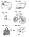
- a semiconductor device can be used broadly, it may be used by being mounted in products such as, bills, coins, securities, bearer bonds, certificates (driver's licenses, resident cards, or the like, see FIG 15A ), containers for wrapping objects (wrapping paper, bottles, or the like, see FIG 15C ), recording media (DVDs, video tapes, or the like, see FIG 15B ), vehicles (bicycles or the like, see FIG 15D ), products such as personal belongings (bags, glasses, or the like), foods, plants, animals, human bodies, clothes, commodities, or electronic devices (a liquid crystal display device, an EL display device, a television device, or a cellular phone), or objects such as shipping tags of products (see FIGS. 15E and 15F ).
- products such as, bills, coins, securities, bearer bonds, certificates (driver's licenses, resident cards, or the like, see FIG 15A ), containers for wrapping objects (wrapping paper, bottles, or the like, see FIG 15C ), recording media (DVD
- a semiconductor device 3000 comprising the present invention is mounted on a printed substrate, attached to a surface, or incorporated to be fixed in an object.
- the semiconductor device is incorporated in paper of a book or an organic resin of a package to be fixed in each object.
- the semiconductor device 3000 comprising the present invention a small size, a thin shape, and lightweight are achieved and an attractive design of the object itself is not damaged even after being fixed in the object.
- the semiconductor device 3000 comprising the present invention being provided in bills, coins, securities, bearer bonds, certificates, or the like, a certification function can be obtained and forgery thereof can be prevented by the use of the certification function being made.
- the semiconductor device 3000 comprising the present invention being provided in containers for wrapping objects, recording media, personal belongings, foods, clothes, commodities, electronic devices, or the like, a system such as an inspection system can be performed efficiently.
- a system such as an inspection system can be performed efficiently.
- the level of security against theft or the like can be raised when the semiconductor device comprising the present invention is attached to the vehicle.
- a CPU (hereinafter referred to as a wireless communication CPU) having a wireless communication function which is formed as an example of a semiconductor device comprising the present invention will be described.
- a wireless communication CPU (hereinafter referred to as a UHF wireless communication CPU) using a wireless signal of a UHF band (915 MHz) will be described.
- a communication standard of the UHF wireless communication CPU is partially based on Auto-ID Center Class I Region 1 (North America).
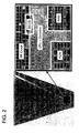
- FIG 2 A photograph of a plastic UHF wireless communication CPU is shown in FIG 2 .
- a V-shaped dipole antenna is used for an antenna and formed externally. Note that, as for a circuit structure of the plastic UHF wireless communication CPU in this embodiment, the description of the block diagram of the circuit structure of Embodiment with reference to figure shown in FIG 3 is referenced here.
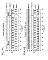
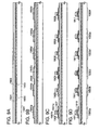
- FIGS. 4A and 4B main signal waveform data of the clock signal generation circuit in the wireless communication CPU of this embodiment is shown in FIGS. 4A and 4B .
- the clock signal (PH) 117 is made up of PH1 and PH2 which are dual-phase non-overlap clocks with a duty ratio of 25%.
- FIG 4A shows signal waveforms of a SYNC period
- FIG. 4B shows signal waveforms of an ASYNC period.
- respective PH1s in FIGS. 4A and 4B are compared, they match each other very well, and when respective PH2s in FIGS. 4A and 4B are compared, they match each other very well. Accordingly, it is found that a clock signal to be generated in the clock signal generation circuit included in the semiconductor device comprising the present invention has an excellent level of stability.
- the CPU 310 in the UHF wireless communication CPU of this embodiment is a CPU of 8-bit CISC architecture.
- the number of clocks per instruction (CPI) could be improved, arithmetic performance was improved by about four times, and a circuit scale was reduced by about 25%. Therefore, while low power consumption could be achieved by setting a clock frequency to about one third (1.12 MHz), arithmetic performance could be improved by about 1.5 times.
- an address area of a control register is physically arranged in the RAM so that a circuit scale of the controller 313 could be reduced by about 30%, compared with the HF wireless communication CPU. Therefore, power consumption could be greatly reduced.
- the ROM 311 in the wireless communication CPU of this embodiment is a mask ROM having a capacity of 4 kB and stores a program, an ID number, or the like.
- low power consumption can be achieved by subdividing a bit line which is precharged at the time of reading.
- the RAM 312 is an SRAM having a capacity of 512 bytes and used as a control register as well as a working area of the CPU 310.
- low power consumption can be achieved by forming a structure in which a memory portion is divided into 16 subblocks and only one subblock is operated at the time of reading/writing.
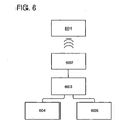
- the measuring system includes a semiconductor device 601, an antenna 602, a circulator 603, a spectrum analyzer 604, and a function generator 605.
- This measurement is performed in such a way that a transmitted signal is generated in the function generator 605 and transmitted as a wireless signal from the antenna 602 via the circulator 603.
- a transmitted signal from the semiconductor device 601 is received by the antenna 602 and input to the spectrum analyzer 604 via the circulator 603.
- the measurement results shown in FIG. 5 are results of a response signal waveform of the CPU having the UHF wireless function formed over a glass substrate which are measured by a spectrum analyzer.
- a communication distance when an antenna output is 30 dBm is 43 cm.
- power consumption by the chip when an internally generated power supply voltage is 1.5 V is 0.54 mW. This is about one seventh of the HF wireless communication CPU, and as a result, it can be said that low power consumption can be achieved.
- a first result 700 is a power consumption of 4.1 mW at the time when a power supply voltage is 1.8 V in the HF wireless communication CPU
- a second result 710 is a power consumption of 0.81 mW at the time when a power supply voltage is 1.8 V in the UHF wireless communication CPU.
- power consumption 701 of the CPU, power consumption 702 of the controller, power consumption 703 of the ROM, and power consumption 704 of the RAM are shown by a bar graph.
- power consumption 711 of the CPU, power consumption 712 of the controller, power consumption 713 of the ROM, power consumption 714 of the RAM, power consumption 715 of the clock signal generation circuit, and power consumption 716 of the constant voltage circuit are shown by a bar graph. Note that the measurement of power consumption is performed in such a way that power consumption of the wireless communication CPU which is formed over a glass substrate is measured and the power consumption in each block is calculated using a ratio by simulation. As shown in FIG 7 , power consumption of the UHF wireless communication CPU is reduced to about one fifth of the power consumption of the HF wireless communication CPU.
- the UHF wireless communication CPU can operate at lower voltage, and a power consumption of 0.54 mW, which is very low, is realized at the minimum operating voltage of 1.5 V As a result, it is found that low power consumption can be realized using the design method used in this embodiment.
- the UHF wireless communication CPU of the present embodiment by use of the clock signal generation circuit, generation of a clock signal having a stable frequency, which is unrelated to variations in the characteristics of TFTs, could be realized.
- operation efficiency of the CPU was improved and low power consumption was realized by control of the active areas of the memories (ROM: read only memory and RAM: random access memory).
- ROM read only memory
- RAM random access memory
- an increase in capacity of the memories was realized while a reduction in chip area was realized.
- a function of resistance to side channel attacks or the like could be implemented by software, and an encoding function could be reinforced.
- a semiconductor device provided with the clock signal generation circuit of the present invention can generate a stable clock signal, and even when wireless communication is employed at the UHF band or the like, for example, a semiconductor device which can realize a stable operation can be provided at low cost.
Landscapes
- Engineering & Computer Science (AREA)
- Theoretical Computer Science (AREA)
- Physics & Mathematics (AREA)
- General Physics & Mathematics (AREA)
- General Engineering & Computer Science (AREA)
- Mathematical Optimization (AREA)
- Computing Systems (AREA)
- Mathematical Analysis (AREA)
- Computational Mathematics (AREA)
- Mathematical Physics (AREA)
- Pure & Applied Mathematics (AREA)
- Computer Networks & Wireless Communication (AREA)
- Signal Processing (AREA)
- Semiconductor Integrated Circuits (AREA)
- Manipulation Of Pulses (AREA)
- Electronic Switches (AREA)
- Stabilization Of Oscillater, Synchronisation, Frequency Synthesizers (AREA)
- Thin Film Transistor (AREA)
Applications Claiming Priority (1)
| Application Number | Priority Date | Filing Date | Title |
|---|---|---|---|
| JP2007029287 | 2007-02-08 |
Publications (2)
| Publication Number | Publication Date |
|---|---|
| EP1956480A1 EP1956480A1 (en) | 2008-08-13 |
| EP1956480B1 true EP1956480B1 (en) | 2012-04-18 |
Family
ID=39401148
Family Applications (1)
| Application Number | Title | Priority Date | Filing Date |
|---|---|---|---|
| EP08001426A Not-in-force EP1956480B1 (en) | 2007-02-08 | 2008-01-25 | Clock signal generation circuit and semiconductor device |
Country Status (4)
| Country | Link |
|---|---|
| US (1) | US7639058B2 (enExample) |
| EP (1) | EP1956480B1 (enExample) |
| JP (1) | JP5204504B2 (enExample) |
| KR (1) | KR101428787B1 (enExample) |
Families Citing this family (20)
| Publication number | Priority date | Publication date | Assignee | Title |
|---|---|---|---|---|
| GB2463074B (en) * | 2008-09-02 | 2010-12-22 | Ip Access Ltd | Communication unit and method for selective frequency synchronisation in a cellular communication network |
| US8386829B2 (en) * | 2009-06-17 | 2013-02-26 | Macronix International Co., Ltd. | Automatic internal trimming calibration method to compensate process variation |
| US20110285421A1 (en) * | 2010-05-24 | 2011-11-24 | Alexander Roger Deas | Synchronous logic system secured against side-channel attack |
| US8427194B2 (en) * | 2010-05-24 | 2013-04-23 | Alexander Roger Deas | Logic system with resistance to side-channel attack by exhibiting a closed clock-data eye diagram |
| KR101162259B1 (ko) * | 2010-12-03 | 2012-07-04 | 에스케이하이닉스 주식회사 | 반도체 집적회로 및 그의 구동 방법 |
| US10191466B2 (en) | 2015-01-28 | 2019-01-29 | Lam Research Corporation | Systems and methods for synchronizing execution of recipe sets |
| US9509318B2 (en) * | 2015-03-13 | 2016-11-29 | Qualcomm Incorporated | Apparatuses, methods, and systems for glitch-free clock switching |
| US10930205B2 (en) | 2016-05-19 | 2021-02-23 | Semiconductor Energy Laboratory Co., Ltd. | Display system and moving object |
| US10867577B2 (en) | 2016-12-23 | 2020-12-15 | Semiconductor Energy Laboratory Co., Ltd. | Display device including data conversion circuit |
| JP6828482B2 (ja) * | 2017-02-08 | 2021-02-10 | オムロン株式会社 | 制御システム、およびパルス出力装置 |
| US10200192B2 (en) | 2017-04-19 | 2019-02-05 | Seagate Technology Llc | Secure execution environment clock frequency hopping |
| US10459477B2 (en) | 2017-04-19 | 2019-10-29 | Seagate Technology Llc | Computing system with power variation attack countermeasures |
| US10270586B2 (en) | 2017-04-25 | 2019-04-23 | Seagate Technology Llc | Random time generated interrupts in a cryptographic hardware pipeline circuit |
| US10771236B2 (en) | 2017-05-03 | 2020-09-08 | Seagate Technology Llc | Defending against a side-channel information attack in a data storage device |
| US10511433B2 (en) | 2017-05-03 | 2019-12-17 | Seagate Technology Llc | Timing attack protection in a cryptographic processing system |
| US11308239B2 (en) | 2018-03-30 | 2022-04-19 | Seagate Technology Llc | Jitter attack protection circuit |
| US10785016B2 (en) | 2018-07-25 | 2020-09-22 | Silicon Laboratories, Inc. | Countermeasure for power injection security attack |
| CN114631145A (zh) | 2019-11-11 | 2022-06-14 | 株式会社半导体能源研究所 | 信息处理装置及信息处理装置的工作方法 |
| US11057001B2 (en) | 2020-06-14 | 2021-07-06 | Intel Corporation | Apparatus, system, and method of distributing a reset signal to a plurality of PHY chains |
| US11762993B2 (en) * | 2021-04-12 | 2023-09-19 | Nxp B.V. | Securing cryptographic operations from side channel attacks using a chaotic oscillator |
Family Cites Families (15)
| Publication number | Priority date | Publication date | Assignee | Title |
|---|---|---|---|---|
| JPH01112819A (ja) * | 1987-10-26 | 1989-05-01 | Fujitsu Ltd | クロック生成回路の動作補償方式 |
| JPH04281617A (ja) * | 1991-03-08 | 1992-10-07 | Victor Co Of Japan Ltd | 基準クロック発生回路 |
| US5155748A (en) * | 1991-04-04 | 1992-10-13 | Zenith Electronics Corporation | Programmable multi-source IR detector |
| JP3181396B2 (ja) | 1992-09-29 | 2001-07-03 | 沖電気工業株式会社 | クロック発生回路 |
| JPH07154243A (ja) * | 1993-11-29 | 1995-06-16 | Mitsubishi Electric Corp | 電子式時計装置ならびに補正値決定装置および方法 |
| US6343364B1 (en) * | 2000-07-13 | 2002-01-29 | Schlumberger Malco Inc. | Method and device for local clock generation using universal serial bus downstream received signals DP and DM |
| JP2002305443A (ja) | 2001-04-06 | 2002-10-18 | Texas Instr Japan Ltd | タイマー回路 |
| JP2003198874A (ja) * | 2001-12-26 | 2003-07-11 | Nec Corp | システムクロック生成回路 |
| US6928127B2 (en) * | 2003-03-11 | 2005-08-09 | Atheros Communications, Inc. | Frequency synthesizer with prescaler |
| US7282937B2 (en) | 2003-12-31 | 2007-10-16 | Intel Corporation | On-chip frequency degradation compensation |
| EP1911160B1 (en) * | 2005-04-27 | 2013-05-29 | Semiconductor Energy Laboratory Co., Ltd. | Pll circuit and semiconductor device having the same |
| JP4823597B2 (ja) | 2005-07-25 | 2011-11-24 | オリンパスメディカルシステムズ株式会社 | 医療用制御装置 |
| EP1748344A3 (en) | 2005-07-29 | 2015-12-16 | Semiconductor Energy Laboratory Co., Ltd. | Semiconductor device |
| EP1873959A3 (en) * | 2006-06-30 | 2012-07-25 | Semiconductor Energy Laboratory Co., Ltd. | Clock synchronization circuit and semiconductor device provided therewith |
| KR101381359B1 (ko) | 2006-08-31 | 2014-04-04 | 가부시키가이샤 한도오따이 에네루기 켄큐쇼 | 클록 생성 회로 및 이 클록 생성 회로를 구비한 반도체장치 |
-
2008
- 2008-01-22 KR KR1020080006679A patent/KR101428787B1/ko not_active Expired - Fee Related
- 2008-01-25 EP EP08001426A patent/EP1956480B1/en not_active Not-in-force
- 2008-01-29 US US12/021,843 patent/US7639058B2/en not_active Expired - Fee Related
- 2008-02-05 JP JP2008025212A patent/JP5204504B2/ja not_active Expired - Fee Related
Also Published As
| Publication number | Publication date |
|---|---|
| EP1956480A1 (en) | 2008-08-13 |
| US20080211561A1 (en) | 2008-09-04 |
| JP5204504B2 (ja) | 2013-06-05 |
| KR20080074730A (ko) | 2008-08-13 |
| KR101428787B1 (ko) | 2014-08-08 |
| JP2008219877A (ja) | 2008-09-18 |
| US7639058B2 (en) | 2009-12-29 |
Similar Documents
| Publication | Publication Date | Title |
|---|---|---|
| EP1956480B1 (en) | Clock signal generation circuit and semiconductor device | |
| EP1986070B1 (en) | Clock signal generation circuit and semiconductor device | |
| US8510588B2 (en) | Clock generation circuit and semiconductor device including the same | |
| EP1873688B1 (en) | Semiconductor device | |
| KR101373532B1 (ko) | 반도체장치 및 상기 반도체장치를 구비하는 전자 장치 | |
| US7663447B2 (en) | Oscillator circuit having a stable output signal resistant to power supply voltage fluctuation | |
| EP1986325B1 (en) | Semiconductor device and driving method thereof | |
| US8374303B2 (en) | Clock synchronization circuit and semiconductor device provided therewith | |
| US8036604B2 (en) | Transmitting and receiving circuit and semiconductor device including the same | |
| JP5063256B2 (ja) | クロック生成回路、クロック生成回路が有するカウンター回路、及び半導体装置 | |
| JP5348859B2 (ja) | 受信回路及び半導体装置 | |
| HK1125504A (en) | Clock signal generation circuit and semiconductor device |
Legal Events
| Date | Code | Title | Description |
|---|---|---|---|
| PUAI | Public reference made under article 153(3) epc to a published international application that has entered the european phase |
Free format text: ORIGINAL CODE: 0009012 |
|
| AK | Designated contracting states |
Kind code of ref document: A1 Designated state(s): AT BE BG CH CY CZ DE DK EE ES FI FR GB GR HR HU IE IS IT LI LT LU LV MC MT NL NO PL PT RO SE SI SK TR |
|
| AX | Request for extension of the european patent |
Extension state: AL BA MK RS |
|
| 17P | Request for examination filed |
Effective date: 20081201 |
|
| 17Q | First examination report despatched |
Effective date: 20090116 |
|
| AKX | Designation fees paid |
Designated state(s): DE FI FR GB NL |
|
| GRAP | Despatch of communication of intention to grant a patent |
Free format text: ORIGINAL CODE: EPIDOSNIGR1 |
|
| RIC1 | Information provided on ipc code assigned before grant |
Ipc: H04L 7/033 20060101ALI20110825BHEP Ipc: G06F 1/04 20060101ALI20110825BHEP Ipc: G06F 1/025 20060101ALI20110825BHEP Ipc: H03K 23/68 20060101ALI20110825BHEP Ipc: H04L 7/08 20060101ALI20110825BHEP Ipc: G06F 1/08 20060101ALI20110825BHEP Ipc: G06F 7/68 20060101AFI20110825BHEP |
|
| GRAS | Grant fee paid |
Free format text: ORIGINAL CODE: EPIDOSNIGR3 |
|
| GRAA | (expected) grant |
Free format text: ORIGINAL CODE: 0009210 |
|
| AK | Designated contracting states |
Kind code of ref document: B1 Designated state(s): DE FI FR GB NL |
|
| REG | Reference to a national code |
Ref country code: GB Ref legal event code: FG4D |
|
| REG | Reference to a national code |
Ref country code: DE Ref legal event code: R096 Ref document number: 602008014837 Country of ref document: DE Effective date: 20120614 |
|
| REG | Reference to a national code |
Ref country code: NL Ref legal event code: VDEP Effective date: 20120418 |
|
| PG25 | Lapsed in a contracting state [announced via postgrant information from national office to epo] |
Ref country code: FI Free format text: LAPSE BECAUSE OF FAILURE TO SUBMIT A TRANSLATION OF THE DESCRIPTION OR TO PAY THE FEE WITHIN THE PRESCRIBED TIME-LIMIT Effective date: 20120418 |
|
| PG25 | Lapsed in a contracting state [announced via postgrant information from national office to epo] |
Ref country code: NL Free format text: LAPSE BECAUSE OF FAILURE TO SUBMIT A TRANSLATION OF THE DESCRIPTION OR TO PAY THE FEE WITHIN THE PRESCRIBED TIME-LIMIT Effective date: 20120418 |
|
| PLBE | No opposition filed within time limit |
Free format text: ORIGINAL CODE: 0009261 |
|
| STAA | Information on the status of an ep patent application or granted ep patent |
Free format text: STATUS: NO OPPOSITION FILED WITHIN TIME LIMIT |
|
| 26N | No opposition filed |
Effective date: 20130121 |
|
| PGFP | Annual fee paid to national office [announced via postgrant information from national office to epo] |
Ref country code: FR Payment date: 20130204 Year of fee payment: 6 Ref country code: GB Payment date: 20130123 Year of fee payment: 6 |
|
| REG | Reference to a national code |
Ref country code: DE Ref legal event code: R097 Ref document number: 602008014837 Country of ref document: DE Effective date: 20130121 |
|
| GBPC | Gb: european patent ceased through non-payment of renewal fee |
Effective date: 20140125 |
|
| REG | Reference to a national code |
Ref country code: FR Ref legal event code: ST Effective date: 20140930 |
|
| PG25 | Lapsed in a contracting state [announced via postgrant information from national office to epo] |
Ref country code: GB Free format text: LAPSE BECAUSE OF NON-PAYMENT OF DUE FEES Effective date: 20140125 Ref country code: FR Free format text: LAPSE BECAUSE OF NON-PAYMENT OF DUE FEES Effective date: 20140131 |
|
| PGFP | Annual fee paid to national office [announced via postgrant information from national office to epo] |
Ref country code: DE Payment date: 20200114 Year of fee payment: 13 |
|
| REG | Reference to a national code |
Ref country code: DE Ref legal event code: R119 Ref document number: 602008014837 Country of ref document: DE |
|
| PG25 | Lapsed in a contracting state [announced via postgrant information from national office to epo] |
Ref country code: DE Free format text: LAPSE BECAUSE OF NON-PAYMENT OF DUE FEES Effective date: 20210803 |