EP1956360B2 - Vorrichtung zur Beobachtung eine Probe und ein Verfahren zur Bereitstellung einer solchen - Google Patents
Vorrichtung zur Beobachtung eine Probe und ein Verfahren zur Bereitstellung einer solchen Download PDFInfo
- Publication number
- EP1956360B2 EP1956360B2 EP06833640.3A EP06833640A EP1956360B2 EP 1956360 B2 EP1956360 B2 EP 1956360B2 EP 06833640 A EP06833640 A EP 06833640A EP 1956360 B2 EP1956360 B2 EP 1956360B2
- Authority
- EP
- European Patent Office
- Prior art keywords
- image
- optical system
- specimen
- forming optical
- imaging
- Prior art date
- Legal status (The legal status is an assumption and is not a legal conclusion. Google has not performed a legal analysis and makes no representation as to the accuracy of the status listed.)
- Ceased
Links
- 238000000034 method Methods 0.000 title claims description 11
- 238000005286 illumination Methods 0.000 claims description 54
- 230000003287 optical effect Effects 0.000 claims description 38
- 238000003384 imaging method Methods 0.000 claims description 23
- 239000004973 liquid crystal related substance Substances 0.000 claims description 10
- 238000009826 distribution Methods 0.000 claims description 7
- 230000000873 masking effect Effects 0.000 claims description 5
- 230000001419 dependent effect Effects 0.000 claims description 2
- 239000011295 pitch Substances 0.000 description 10
- 230000004048 modification Effects 0.000 description 3
- 238000012986 modification Methods 0.000 description 3
- 210000001747 pupil Anatomy 0.000 description 3
- 238000010586 diagram Methods 0.000 description 2
- 239000011521 glass Substances 0.000 description 1
- 230000003760 hair shine Effects 0.000 description 1
- 230000010363 phase shift Effects 0.000 description 1
- 239000012780 transparent material Substances 0.000 description 1
Images


Classifications
-
- G—PHYSICS
- G01—MEASURING; TESTING
- G01N—INVESTIGATING OR ANALYSING MATERIALS BY DETERMINING THEIR CHEMICAL OR PHYSICAL PROPERTIES
- G01N21/00—Investigating or analysing materials by the use of optical means, i.e. using sub-millimetre waves, infrared, visible or ultraviolet light
- G01N21/17—Systems in which incident light is modified in accordance with the properties of the material investigated
-
- G—PHYSICS
- G02—OPTICS
- G02B—OPTICAL ELEMENTS, SYSTEMS OR APPARATUS
- G02B21/00—Microscopes
- G02B21/0004—Microscopes specially adapted for specific applications
-
- G—PHYSICS
- G01—MEASURING; TESTING
- G01N—INVESTIGATING OR ANALYSING MATERIALS BY DETERMINING THEIR CHEMICAL OR PHYSICAL PROPERTIES
- G01N21/00—Investigating or analysing materials by the use of optical means, i.e. using sub-millimetre waves, infrared, visible or ultraviolet light
- G01N21/17—Systems in which incident light is modified in accordance with the properties of the material investigated
- G01N21/47—Scattering, i.e. diffuse reflection
- G01N21/4738—Diffuse reflection, e.g. also for testing fluids, fibrous materials
-
- G—PHYSICS
- G01—MEASURING; TESTING
- G01N—INVESTIGATING OR ANALYSING MATERIALS BY DETERMINING THEIR CHEMICAL OR PHYSICAL PROPERTIES
- G01N21/00—Investigating or analysing materials by the use of optical means, i.e. using sub-millimetre waves, infrared, visible or ultraviolet light
- G01N21/17—Systems in which incident light is modified in accordance with the properties of the material investigated
- G01N21/47—Scattering, i.e. diffuse reflection
- G01N21/4788—Diffraction
-
- G—PHYSICS
- G02—OPTICS
- G02B—OPTICAL ELEMENTS, SYSTEMS OR APPARATUS
- G02B21/00—Microscopes
- G02B21/06—Means for illuminating specimens
-
- G—PHYSICS
- G02—OPTICS
- G02B—OPTICAL ELEMENTS, SYSTEMS OR APPARATUS
- G02B21/00—Microscopes
- G02B21/06—Means for illuminating specimens
- G02B21/08—Condensers
- G02B21/12—Condensers affording bright-field illumination
- G02B21/125—Condensers affording bright-field illumination affording both dark- and bright-field illumination
-
- G—PHYSICS
- G02—OPTICS
- G02B—OPTICAL ELEMENTS, SYSTEMS OR APPARATUS
- G02B21/00—Microscopes
- G02B21/06—Means for illuminating specimens
- G02B21/08—Condensers
- G02B21/14—Condensers affording illumination for phase-contrast observation
-
- G—PHYSICS
- G01—MEASURING; TESTING
- G01N—INVESTIGATING OR ANALYSING MATERIALS BY DETERMINING THEIR CHEMICAL OR PHYSICAL PROPERTIES
- G01N21/00—Investigating or analysing materials by the use of optical means, i.e. using sub-millimetre waves, infrared, visible or ultraviolet light
- G01N21/17—Systems in which incident light is modified in accordance with the properties of the material investigated
- G01N21/47—Scattering, i.e. diffuse reflection
- G01N21/4738—Diffuse reflection, e.g. also for testing fluids, fibrous materials
- G01N2021/4764—Special kinds of physical applications
- G01N2021/4773—Partly or totally translucent samples
-
- G—PHYSICS
- G01—MEASURING; TESTING
- G01N—INVESTIGATING OR ANALYSING MATERIALS BY DETERMINING THEIR CHEMICAL OR PHYSICAL PROPERTIES
- G01N21/00—Investigating or analysing materials by the use of optical means, i.e. using sub-millimetre waves, infrared, visible or ultraviolet light
- G01N21/84—Systems specially adapted for particular applications
- G01N21/88—Investigating the presence of flaws or contamination
- G01N21/8806—Specially adapted optical and illumination features
- G01N2021/8822—Dark field detection
-
- G—PHYSICS
- G02—OPTICS
- G02B—OPTICAL ELEMENTS, SYSTEMS OR APPARATUS
- G02B21/00—Microscopes
- G02B21/36—Microscopes arranged for photographic purposes or projection purposes or digital imaging or video purposes including associated control and data processing arrangements
Definitions
- the present invention relates to an observing apparatus for observing a transparent specimen.
- Non-patent Documents 1 and 2 To observe a transparent specimen such as cells in a culture container, the phase contrast observation (refer to Non-patent Documents 1 and 2, for example) which can visualize its refractive index distribution is used suitably.
- a microscope or some other optical system To observe a transparent specimen which cannot be observed with naked eyes, a microscope or some other optical system is necessary even if the observation is intended to check the entire specimen roughly.
- NON-patent Document 1 Hiroshi Komatsu, "Fundamentals and Applications of Optical Microscopes (3)," Applied Physics, Vol. 60, No. 19, pp. 1,032-1,034, 1991
- NON-patent Document 2 Hiroshi Komatsu, “Fundamentals and Applications of Optical Microscopes (4)," Applied Physics, Vol. 60, No. 11, pp. 1,136-1,138, 1991
- phase contrast microscopes having such a wide field of view as to enable observation of the entire area of a culture container at one time. If one attempted to realize such a phase contrast microscope, it would be extremely costly because a very large image-forming optical system for phase contrast observation and a very large zonal illuminating optical system are necessary.
- dark-field observation To observe the entire specimen only roughly, one option is to perform dark-field observation instead of phase contrast observation.
- dark-field observation faint diffraction light (scattered light) generated by refractive index bounds in a specimen is detected and an observation image is formed by using only the diffraction light.
- the illumination angle is increased and an observation image can only be formed from very faint diffraction light that is emitted from a specimen at large angles. Therefore, the brightness of the observation image is far too low. Furthermore, where the illumination angle is large, there may occur a case that strong light generated by the edge, bottom, or the like of a culture container enters the image-forming optical system and obstructs the observation.
- An object of the present invention is therefore to provide an observing apparatus suitable to observe a transparent specimen with a wide field of view.
- JP 2002311335 relates to a grating illumination microscope with an illumination optical system and a one-dimensional grating for illuminating a specimen.
- the invention realizes an observing apparatus suitable to observe a transparent specimen with a wide field of view.
- This embodiment is an embodiment of an observing apparatus.
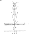
- Fig. 1 shows the entire configuration of this observing apparatus.
- this observing apparatus is equipped with a transmission-type liquid crystal panel 14 having a backlight, a stage (table for a specimen) 13, an image-forming optical system 12, an imaging sensor 11, a controller 15 for the transmission-type liquid crystal panel, a computer 16, a display 17, etc.
- a transparent observation object 10 is placed on the stage 13.
- the observation object 10 is a transparent culture container (e.g., a petri dish of 35 mm in diameter) containing unstained cells.
- the transmission-type liquid crystal panel 14 illuminates approximately the entire area of the observation object 10. So as not to interrupt illumination light, the portion of the stage 13 on which the observation object 10 is placed is made of a transparent material such as glass or is made hollow.
- the image-forming optical system 12 has a sufficiently wide field of view, and light emitted from approximately the entire area of the observation object 10 is collected by the image-forming optical system 12 and image-formed on the imaging plane of the imaging sensor 11.
- the image sensor 11 picks up an image (brightness distribution) on the imaging plane according to an instruction from the computer 16.
- the image is taken in by the computer 16 and displayed on the display 17 after being subjected to image processing.
- the computer 16 can store an image that has or has not been subjected to image processing.
- an image that has not been subjected to image processing can be displayed on the display 17.
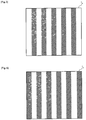
- the controller 15 displays, on the transmission-type liquid crystal panel 14, a pattern in which bright areas and dark areas are arranged alternately.
- this pattern is a striped pattern.
- a striped surface illumination pattern is formed on the transmission-type liquid crystal panel 14.
- the pitch P of contrasting of this surface illumination pattern is sufficiently longer than the size (10 to 15 ⁇ m) of a phase object (cells) as a subject of observation, and the distance d between the surface illumination pattern and the observation object 10 is properly so long that the surface illumination pattern is out of the depth of field of the image-forming optical system 12.
- the relationship between the pitch P and the distance d is set so as to satisfy the following three conditions.
- the display pattern on the transmission-type liquid crystal panel 14 may be either a binary pattern or a grayscale pattern.
- Fig. 2 is a conceptual diagram illustrating the operation of an optical system part of this observing apparatus.
- Fig. 2 conceptually shows the optical system part of this observing apparatus.
- Light beams LB and LC that are emitted from two respective bright areas 14B and 14C that are adjacent to the dark area 14A shine on the partial area 10A. No light beam coming from the dark area 14A shines on the partial area 10A. Therefore, the partial area 10A is illuminated obliquely by the light beams LB and LC.
- an image of the dark area 14A and an image (hereinafter referred to as "observation image") of the outline of a phase object existing in the partial area 10A are formed in superimposition in an area 11A on the imaging sensor 11 that is conjugate with the partial area 10A. That is, a dark-field image of the partial area 10A is formed.
- the angle that is subtended at the partial area 10A by the two bright areas 14B and 14C is sufficiently small. Therefore, the angles at which the area 10A is illuminated with the light beams LB and LC are also sufficiently small.
- the observation image of the partial area 10A is generated by the high-intensity diffraction lights Lb and Lc that are emitted at small angles. Therefore, the observation image of the partial area 10A is sufficiently bright.
- an image I 1 acquired by the imaging sensor 11 is such that an observation image is superimposed on a striped dark background.
- the boundaries between the bright portions and the dark portions of the surface illumination pattern image are drawn as sharp lines, they are blurred actually.
- a user can easily observe the observation object 10 by displaying the image I 1 on the display 17 by the computer 16.
- the image I 1 includes only the observation image of the areas that account for about a half of the total area of the observation object 10 (i.e., only the observation image of the areas that are squarely opposed to the dark areas). Furthermore, the contrast of the observation image is low because the background of the observation image is not a complete dark background and has a sinusoidal brightness distribution.
- the computer 16 of this observing apparatus executes the following process to allow an approximately entire area of the observation object 10 to be observed with high contrast.
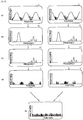
- Step 1 Displays a striped surface illumination pattern (duty ratio: 50%) on the transmission-type liquid crystal panel 14 and acquires an image I 1 as shown in Fig. 3 in this state.
- Step 2 Shifts the phase of contrasting of the surface illumination pattern by ⁇ and acquires an image I 2 as shown in Fig. 4 in this state.
- the image I 2 includes an observation image of different areas from the image I 1 does.
- Fig. 5(a) conceptually shows brightness distributions of the images I 1 and I 2 in the direction of the pitch of contrasting.
- Step 3 As shown in Figs. 5(a) and 5(b) , performs spatial Fourier transform on the images I 1 and I 2 individually and thereby obtains data D 1 representing spatial frequency components of the image h and data D 2 representing spatial frequency components of the image I 2 .
- the large peak on the low frequency side is a component of the surface illumination pattern image and plural small peaks on the high frequency side are components of the observation image.
- Step 4 As shown in Figs. 5(b) and 5(c) , removes the component of the surface illumination pattern image from each of the data D 1 and D 2 and thereby obtains data D 1 ' and D 2 '.
- Step 5 As shown in Figs. 5(c) and 5(d) , performs inverse Fourier transform on the data D 1 ' and D 2 ' individually and thereby obtains images I 1 ' and I 2 '.
- Each of the images I 1 ' and I 2 ' includes only the observation image, that is, it does not include the surface illumination pattern image.
- Step 6 As shown in Figs. 5(d) and 5(e) , combines the images I 1 ' and I 2 ' together and thereby obtains a single image I.
- the image I is displayed on the display 17.
- the image I includes an observation image of an approximately entire area of the observation object 10 and its background is black. Therefore, a user can observe the approximately entire area of the observation object 10 with high contrast as a dark-field image.
- Step 1 Displays a striped surface illumination pattern (duty ratio: 50%) on the transmission-type liquid crystal panel 14 and acquires an image I 1 as shown in Fig. 6(a) in this state.
- Step 2 Shifts the phase of contrasting of the surface illumination pattern by 2 ⁇ /3 and acquires an image I 2 as shown in Fig. 6(b) in this state.
- Step 3 Shifts the phase of contrasting of the surface illumination pattern further by 2 ⁇ /3 and acquires an image I 3 as shown in Fig. 6(c) in this state.
- Step 4 Obtains a single image I as shown in Fig. 6(d) by substituting the images I 1 , I 2 , and I 3 into the following calculation formula (1) on a pixel-by-pixel basis.
- I I 1 ⁇ I 2 2 + I 2 ⁇ I 3 2 + I 3 ⁇ I 1 2
- the image I includes an observation image of an approximately entire area of the observation object 10 and its background is uniform in brightness.
- the computer 16 removes, from the image I, the component (0th component) whose spatial frequency is zero.
- the computer 16 displays a resulting image on the display 17.
- the resulting image includes an observation image of an approximately entire area of the observation object 10 and its background is black. Therefore, a user can observe the approximately entire area of the observation object 10 with high contrast as a dark-field image.
- Fig. 7 illustrates the conditions 1, 2, and 3.
- reference symbol 11a denotes an imaging plane of the imaging sensor 11
- symbol 10a denotes a focal plane (i.e., observation plane) of the image-forming optical system 12
- symbol 14a denotes a plane on which a surface illumination pattern is formed (i.e., light source plane).
- the angle that is subtended at a point on the observation plane 10a by a dark area 14A and a bright area 14C is represented by ⁇ .
- the angle ⁇ corresponds to the incident angle of two light beams LC and LB which shine on the observation plane 10a.
- Characters NA represent the object-side numerical aperture of the image-forming optical system 12, and approximation is possible by regarding it as sufficiently small.
- Inequality (9) is a condition formula corresponding to the condition 1.
- NA' is the image-side numerical aperture of the image-forming optical system 12.
- Inequality (12) is obtained by substituting Equation (10) into Inequality (11): P d ⁇ 2 ⁇ NA ′
- Inequality (12) is a condition formula corresponding to the condition 2.
- magnification M of the image-forming optical system 12 and the light source wavelength ⁇ need to satisfy Inequality (13): P ⁇ M ⁇ ⁇ 2 ⁇ NA
- Inequality (16) is a condition formula corresponding to the condition 3.
- each embodiment employs the controller and the transmission-type liquid crystal panel having a backlight to generate a surface illumination pattern
- other devices may be used as long as they can generate a similar surface illumination pattern.
- many small light sources such as LEDs are prepared and arranged densely in array form, whereby a surface illumination pattern which emits light with an approximately uniform intensity distribution is formed.
- a masking member having striped apertures is disposed on the surface illumination pattern.
- a striped surface illumination pattern is formed.
- the phase of contrasting of the surface illumination pattern can be shifted by shifting the masking member in the direction of the pitch of contrasting.
- plural masking members having different aperture patterns may be prepared and switched.
- the pitch of contrasting of the surface illumination pattern is fixed, the pitch may be varied according to the size of a phase object (cells) as a subject of observation. This makes it possible to properly observe phase objects (cells) having various sizes.
- the duty ratio of contrasting of the surface illumination pattern may be varied according to the refractive index of a phase object (cells) as a subject of observation.
- the proportion of dark areas may be increased (e.g., to 70% or 80%) to decrease the number of times of image acquisition accordingly. This is because an observation image in the same image occupies a larger area when the proportion of dark areas is high.
- the refractive index of a phase object (cells) is small, it is possible to decrease the proportion of dark areas (e.g., to 30%) and increase the number of times of image acquisition accordingly.
- the bright/dark pattern of the surface illumination pattern is a striped pattern
- other patterns may be employed in which bright areas and dark areas are arranged alternately.
- a checkered pattern as shown in Fig. 8 may be employed.
- a concentric pattern as shown in Fig. 9 may also be employed. In either case, the phase of contrasting can be shifted by varying the pattern in such a direction that the bright areas and the dark areas are reversed (in the radial direction in the case of the concentric pattern).
- the employment of the striped pattern ( Fig. 1 ) or the checkered pattern ( Fig. 8 ) is preferable because it simplifies the phase shift processing and the image processing.
Landscapes
- Physics & Mathematics (AREA)
- Chemical & Material Sciences (AREA)
- Analytical Chemistry (AREA)
- General Physics & Mathematics (AREA)
- Optics & Photonics (AREA)
- Life Sciences & Earth Sciences (AREA)
- Health & Medical Sciences (AREA)
- Biochemistry (AREA)
- General Health & Medical Sciences (AREA)
- Immunology (AREA)
- Pathology (AREA)
- Microscoopes, Condenser (AREA)
- Investigating Or Analysing Materials By Optical Means (AREA)
Claims (13)
- Beobachtungsvorrichtung, die Folgendes umfasst:eine Beleuchtungseinheit (14), umfassend ein Beleuchtungsmuster, das sich an einer Beleuchtungsfläche befindet, und in dem helle Bereiche und dunkle Bereiche abwechselnd angeordnet sind;ein bildbildendes optisches System (12), das ein Bild des Lichts bildet, das eine direkt von der Beleuchtungseinheit beleuchtete Probe auf einer objektseitigen Beobachtungsebene (10a) des bildbildenden optischen Systems durchläuft; undeine Abbildungseinheit (11), umfassend eine Abbildungsfläche (1 la) zum Abbilden der Probe, wodurch die Abbildungsfläche in Bezug auf das bildbildende optische System (12) zu der Beobachtungsebene konjugiert ist,
wobei eine Teilung des Kontrastierens des Beleuchtungsmusters veränderbar ist. - Beobachtungsvorrichtung nach Anspruch 1, wobei:
ein Abstand "d" zwischen der Beleuchtungsfläche und der objektseitigen Beobachtungsebene (10a) des bildbildenden optischen Systems (12), eine Teilung "P" zwischen den hellen Bereichen oder zwischen den dunklen Bereichen der Beleuchtungsfläche, NA, welche eine objektseitige numerische Apertur des bildbildenden optischen Systems ist, NA', welche eine bildseitige numerische Apertur des bildbildenden optischen Systems ist, eine Wellenlänge "λ" des Lichts von der Beleuchtungsfläche und ein Abstand "a" zwischen einer bildseitigen Hauptebene des bildbildenden optischen Systems und der Abbildungsfläche (11a) mindestens eine der drei untenstehenden Bedingungen erfüllen: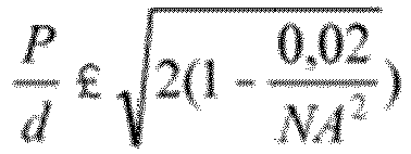


- Beobachtungsvorrichtung nach Anspruch 1 oder Anspruch 2, wobei die Beleuchtungseinheit Folgendes umfasst:eine Flächenbeleuchtungseinheit (14), die Licht mit einer ungefähr gleichmäßigen Intensitätsverteilung ausstrahlt; undeine Abdeckmaske, die auf der Flächenbeleuchtungseinheit angeordnet ist, und in der Aperturbereiche und Abdeckbereiche abwechselnd angeordnet sind.
- Beobachtungsvorrichtung nach einem der Ansprüche 1 bis 3, wobei die Beleuchtungseinheit (14) einen räumlichen Flüssigkristall-Lichtmodulator umfasst.
- Beobachtungsvorrichtung nach einem der Ansprüche 1 bis 4, weiter umfassend eine Bildverarbeitungseinheit (16), die eine Komponente eines Bilds der Beleuchtungsfläche aus dem von der Abbildungseinheit (11) erfassten Bild der Probe entfernt.
- Beobachtungsvorrichtung nach einem der Ansprüche 1 bis 5, weiter umfassend eine Einheit (15), die eine Phase des Kontrastierens des Beleuchtungsmusters verändert.
- Beobachtungsvorrichtung nach einem der Ansprüche 1 bis 6, weiter umfassend eine Einheit (15), die eine Teilung des Kontrastierens des Beleuchtungsmusters verändert.
- Beobachtungsvorrichtung nach einem der Ansprüche 1 bis 7, weiter umfassend eine Einheit (15), die ein Tastverhältnis des Kontrastierens des Beleuchtungsmusters verändert.
- Beobachtungsvorrichtung nach Anspruch 2 oder einem der von Anspruch 2 abhängigen Ansprüche 3 bis 8, umfassend eine Probe, die auf der objektseitigen Beobachtungsebene (10a) des bildbildenden optischen Systems angeordnet ist, wodurch der Abstand "d" der Abstand zwischen der Beleuchtungsfläche und der Probe ist.
- Verfahren zum Bereitstellen einer Beobachtungsvorrichtung zum Beobachten einer Probe, umfassend das Bereitstellen von:einer Beleuchtungseinheit (14), umfassend ein Beleuchtungsmuster, das sich an einer Beleuchtungsfläche befindet, und in dem helle Bereiche und dunkle Bereiche abwechselnd angeordnet sind;einem bildbildenden optischen System (12), das ein Bild des Lichts bildet, das eine direkt von der Beleuchtungseinheit beleuchtete Probe auf einer objektseitigen Beobachtungsebene (10a) des bildbildenden optischen Systems (12) durchläuft; undeiner Abbildungseinheit (11), umfassend eine Abbildungsfläche (11a) zum Abbilden der Probe, wodurch die Abbildungsfläche in Bezug auf das bildbildende optische System (12) zu der Beobachtungsebene konjugiert ist,
wobei die Teilung des Kontrastierens des Beleuchtungsmusters veränderbar ist. - Verfahren nach Anspruch 10, weiter umfassend das Bereitstellen einer Probe auf der Beobachtungsebene.
- Verfahren nach Anspruch 10 oder Anspruch 11, weiter umfassend das Bereitstellen einer Vorrichtung nach einem der Ansprüche 1 bis 9.
- Verfahren nach einem der Ansprüche 10 bis 12, weiter umfassend das Beleuchten und das Abbilden der Probe.
Applications Claiming Priority (2)
| Application Number | Priority Date | Filing Date | Title |
|---|---|---|---|
| JP2005345418 | 2005-11-30 | ||
| PCT/JP2006/323837 WO2007063909A1 (ja) | 2005-11-30 | 2006-11-29 | 観察装置 |
Publications (4)
| Publication Number | Publication Date |
|---|---|
| EP1956360A1 EP1956360A1 (de) | 2008-08-13 |
| EP1956360A4 EP1956360A4 (de) | 2013-02-20 |
| EP1956360B1 EP1956360B1 (de) | 2018-01-24 |
| EP1956360B2 true EP1956360B2 (de) | 2020-12-02 |
Family
ID=38092242
Family Applications (1)
| Application Number | Title | Priority Date | Filing Date |
|---|---|---|---|
| EP06833640.3A Ceased EP1956360B2 (de) | 2005-11-30 | 2006-11-29 | Vorrichtung zur Beobachtung eine Probe und ein Verfahren zur Bereitstellung einer solchen |
Country Status (5)
| Country | Link |
|---|---|
| US (1) | US8400710B2 (de) |
| EP (1) | EP1956360B2 (de) |
| KR (1) | KR20080075123A (de) |
| CN (1) | CN101305275B (de) |
| WO (1) | WO2007063909A1 (de) |
Families Citing this family (17)
| Publication number | Priority date | Publication date | Assignee | Title |
|---|---|---|---|---|
| GB0906449D0 (en) * | 2009-04-15 | 2009-05-20 | Phase Focus Ltd | Improvements in imaging |
| CN101770070B (zh) * | 2009-12-31 | 2016-09-07 | 上海杰远环保科技有限公司 | 观测微型对象的探测仪及操作方法 |
| US9743020B2 (en) | 2010-03-23 | 2017-08-22 | California Institute Of Technology | Super resolution optofluidic microscopes for 2D and 3D imaging |
| US9643184B2 (en) | 2010-10-26 | 2017-05-09 | California Institute Of Technology | e-Petri dishes, devices, and systems having a light detector for sampling a sequence of sub-pixel shifted projection images |
| US9569664B2 (en) | 2010-10-26 | 2017-02-14 | California Institute Of Technology | Methods for rapid distinction between debris and growing cells |
| CN103154662A (zh) * | 2010-10-26 | 2013-06-12 | 加州理工学院 | 扫描投影无透镜显微镜系统 |
| CN103534627A (zh) | 2011-03-03 | 2014-01-22 | 加州理工学院 | 光导像素 |
| JP5955356B2 (ja) * | 2014-08-01 | 2016-07-20 | 株式会社豊田中央研究所 | 照明装置 |
| CN105158888B (zh) * | 2015-09-29 | 2020-09-11 | 南京理工大学 | 基于lcd液晶面板的可编程显微镜聚光镜装置及其成像方法 |
| KR102368587B1 (ko) * | 2015-10-21 | 2022-03-02 | 삼성전자주식회사 | 검사 장치, 그를 포함하는 반도체 소자의 제조 시스템, 및 반도체 소자의 제조 방법 |
| JP6320436B2 (ja) * | 2016-01-15 | 2018-05-09 | 株式会社Screenホールディングス | 撮像装置および撮像方法 |
| CN107203034B (zh) * | 2016-03-18 | 2021-02-26 | 松下知识产权经营株式会社 | 图像生成装置、图像生成方法以及记录介质 |
| US10607316B2 (en) * | 2016-07-22 | 2020-03-31 | Panasonic Intellectual Property Management Co., Ltd. | Image generating apparatus and image generating method |
| CN110023950B (zh) | 2016-10-28 | 2023-08-08 | 拜克门寇尔特公司 | 物质准备评估系统 |
| JP7026333B2 (ja) | 2017-03-01 | 2022-02-28 | パナソニックIpマネジメント株式会社 | 画像生成装置及び画像生成方法 |
| CN111338071A (zh) * | 2020-03-27 | 2020-06-26 | 肯维捷斯(武汉)科技有限公司 | 一种显微成像系统 |
| EP3958036B1 (de) * | 2020-08-20 | 2025-01-15 | Carl Zeiss Microscopy GmbH | Verfahren und vorrichtung zum erzeugen eines übersichtskontrastbildes eines probenträgers in einem mikroskop |
Citations (12)
| Publication number | Priority date | Publication date | Assignee | Title |
|---|---|---|---|---|
| US5617203A (en) † | 1993-10-01 | 1997-04-01 | Hamamatsu Photonics K.K. | Optical detector employing an optically-addressed spatial light modulator |
| US6239909B1 (en) † | 1997-12-25 | 2001-05-29 | Olympus Optical Co. Ltd. | Image-forming method and image-forming apparatus |
| US6243197B1 (en) † | 1996-10-25 | 2001-06-05 | Leica Mikroskopie Und Systeme Gmbh | Lighting device for a microscope |
| WO2002012945A2 (de) † | 2000-08-08 | 2002-02-14 | Carl Zeiss Jena Gmbh | Anordnung zur erhöhung der tiefendiskriminierung optisch abbildender system |
| JP2002189174A (ja) † | 2000-12-20 | 2002-07-05 | Olympus Optical Co Ltd | 顕微鏡用照明装置 |
| US20020125435A1 (en) † | 2001-01-19 | 2002-09-12 | Cofer Darren D. | Method and apparatus for detecting objects |
| JP2002311335A (ja) † | 2001-04-12 | 2002-10-23 | Nikon Corp | 格子照明顕微鏡 |
| WO2002102128A1 (de) † | 2001-06-12 | 2002-12-19 | Siemens Aktiengesellschaft | Optische sensorvorrichtung |
| DE20203462U1 (de) † | 2002-03-04 | 2003-07-10 | febit ag, 68167 Mannheim | Einrichtung zur Belichtung eines insbesondere optofluidischen Reaktionsträgers |
| US6633338B1 (en) † | 1999-04-27 | 2003-10-14 | Gsi Lumonics, Inc. | Programmable illuminator for vision system |
| DE10250568A1 (de) † | 2002-10-28 | 2004-05-13 | Carl Zeiss Jena Gmbh | Verfahren zur Verbesserung der Tiefendiskriminierung optisch abbildender Systeme |
| US20040105575A1 (en) † | 2001-10-18 | 2004-06-03 | Ganz Brian L. | Computer controllable LED light source for device for inspecting microscopic objects |
Family Cites Families (17)
| Publication number | Priority date | Publication date | Assignee | Title |
|---|---|---|---|---|
| US2105671A (en) * | 1935-03-23 | 1938-01-18 | Leitz Ernst Gmbh | Microscope |
| US5548441A (en) * | 1991-04-19 | 1996-08-20 | Edge Scientific Instrument Corp. | Illumination system and method for a high definition light microscope |
| EP0562133B1 (de) * | 1992-03-23 | 1998-02-25 | Erland Torbjörn Sandström | Verfahren und Vorrichtung zur Erzeugung eines Bildes |
| US5751475A (en) * | 1993-12-17 | 1998-05-12 | Olympus Optical Co., Ltd. | Phase contrast microscope |
| US5673144A (en) * | 1994-09-14 | 1997-09-30 | International Business Machines, Corporation | Oblique viewing microscope system |
| JPH11337828A (ja) | 1998-05-28 | 1999-12-10 | Kisutemu Kk | 水中顕微鏡 |
| KR100443143B1 (ko) * | 2000-03-06 | 2004-08-04 | 올림푸스 가부시키가이샤 | 섹셔닝상 관찰장치에 적용되는 패턴형성부재 및 그것을이용한 섹셔닝상 관찰장치 |
| JP2002182008A (ja) | 2000-10-04 | 2002-06-26 | Sharp Corp | 光学レンズシステム、画像表示装置、マイクロレンズアレイ、液晶表示素子および投影型液晶表示装置 |
| JP2003075725A (ja) * | 2001-09-04 | 2003-03-12 | Olympus Optical Co Ltd | 透過照明装置 |
| JP4844862B2 (ja) * | 2001-09-14 | 2011-12-28 | 株式会社ニコン | 格子照明顕微鏡 |
| JPWO2004036284A1 (ja) * | 2002-09-30 | 2006-02-16 | 独立行政法人科学技術振興機構 | 共焦点顕微鏡、共焦点顕微鏡を用いた蛍光測定方法及び偏光測定方法 |
| DE10257521B4 (de) * | 2002-12-10 | 2017-03-30 | Leica Microsystems Cms Gmbh | Auflichtmikroskop |
| JP2004309702A (ja) * | 2003-04-04 | 2004-11-04 | Olympus Corp | 顕微鏡 |
| US7471435B2 (en) * | 2004-02-24 | 2008-12-30 | Modavis Robert A | Apodization technique for enhanced resolution of images |
| JP2006171025A (ja) | 2004-12-10 | 2006-06-29 | Olympus Corp | 照明装置 |
| JP4538633B2 (ja) | 2005-03-29 | 2010-09-08 | 国立大学法人浜松医科大学 | Dlp式スリット光走査顕微鏡 |
| US7345754B1 (en) * | 2005-09-16 | 2008-03-18 | Kla-Tencor Technologies Corp. | Fourier filters and wafer inspection systems |
-
2006
- 2006-11-29 US US12/085,197 patent/US8400710B2/en not_active Expired - Fee Related
- 2006-11-29 KR KR1020087012332A patent/KR20080075123A/ko not_active Withdrawn
- 2006-11-29 WO PCT/JP2006/323837 patent/WO2007063909A1/ja not_active Ceased
- 2006-11-29 EP EP06833640.3A patent/EP1956360B2/de not_active Ceased
- 2006-11-29 CN CN2006800422524A patent/CN101305275B/zh not_active Expired - Fee Related
Patent Citations (12)
| Publication number | Priority date | Publication date | Assignee | Title |
|---|---|---|---|---|
| US5617203A (en) † | 1993-10-01 | 1997-04-01 | Hamamatsu Photonics K.K. | Optical detector employing an optically-addressed spatial light modulator |
| US6243197B1 (en) † | 1996-10-25 | 2001-06-05 | Leica Mikroskopie Und Systeme Gmbh | Lighting device for a microscope |
| US6239909B1 (en) † | 1997-12-25 | 2001-05-29 | Olympus Optical Co. Ltd. | Image-forming method and image-forming apparatus |
| US6633338B1 (en) † | 1999-04-27 | 2003-10-14 | Gsi Lumonics, Inc. | Programmable illuminator for vision system |
| WO2002012945A2 (de) † | 2000-08-08 | 2002-02-14 | Carl Zeiss Jena Gmbh | Anordnung zur erhöhung der tiefendiskriminierung optisch abbildender system |
| JP2002189174A (ja) † | 2000-12-20 | 2002-07-05 | Olympus Optical Co Ltd | 顕微鏡用照明装置 |
| US20020125435A1 (en) † | 2001-01-19 | 2002-09-12 | Cofer Darren D. | Method and apparatus for detecting objects |
| JP2002311335A (ja) † | 2001-04-12 | 2002-10-23 | Nikon Corp | 格子照明顕微鏡 |
| WO2002102128A1 (de) † | 2001-06-12 | 2002-12-19 | Siemens Aktiengesellschaft | Optische sensorvorrichtung |
| US20040105575A1 (en) † | 2001-10-18 | 2004-06-03 | Ganz Brian L. | Computer controllable LED light source for device for inspecting microscopic objects |
| DE20203462U1 (de) † | 2002-03-04 | 2003-07-10 | febit ag, 68167 Mannheim | Einrichtung zur Belichtung eines insbesondere optofluidischen Reaktionsträgers |
| DE10250568A1 (de) † | 2002-10-28 | 2004-05-13 | Carl Zeiss Jena Gmbh | Verfahren zur Verbesserung der Tiefendiskriminierung optisch abbildender Systeme |
Non-Patent Citations (2)
| Title |
|---|
| M.A.A. NEIL ET AL.: "METHOD OF OBTAINING OPTICAL SECTIONING BY USING STRUCTURED LIGHT IN A CONVENTIONAL MICROSCOPE", OPTICS LETTERS, vol. 22, no. 24, 15 December 1997 (1997-12-15), pages 1905 - 1907 † |
| Maschinelle Übersetzung von D10 † |
Also Published As
| Publication number | Publication date |
|---|---|
| EP1956360A1 (de) | 2008-08-13 |
| EP1956360B1 (de) | 2018-01-24 |
| US8400710B2 (en) | 2013-03-19 |
| WO2007063909A1 (ja) | 2007-06-07 |
| EP1956360A4 (de) | 2013-02-20 |
| CN101305275B (zh) | 2010-08-18 |
| KR20080075123A (ko) | 2008-08-14 |
| US20090273829A1 (en) | 2009-11-05 |
| CN101305275A (zh) | 2008-11-12 |
Similar Documents
| Publication | Publication Date | Title |
|---|---|---|
| EP1956360B2 (de) | Vorrichtung zur Beobachtung eine Probe und ein Verfahren zur Bereitstellung einer solchen | |
| JP6062858B2 (ja) | 光学測定方法および光学測定装置 | |
| Li et al. | Efficient quantitative phase microscopy using programmable annular LED illumination | |
| Fahrbach et al. | A line scanned light-sheet microscope with phase shaped self-reconstructing beams | |
| US6239909B1 (en) | Image-forming method and image-forming apparatus | |
| US9599805B2 (en) | Optical imaging system using structured illumination | |
| DE69901516T2 (de) | Vorrichtung zur abtastung einer wellenfront | |
| EP3255414A1 (de) | 3d-brechungsindex-tomographie und strukturiertes beleuchtungsmikroskopiesystem mit verwendung von wellenfrontformer und verfahren dafür | |
| EP3712596A1 (de) | Verfahren zur erzeugung eines quantitativen phasenbildes, vorrichtung zur erzeugung eines quantitativen phasenbildes und programm | |
| EP2919055A1 (de) | Lichtbestrahlungsvorrichtung | |
| US20180088305A1 (en) | Converter, illuminator, and light sheet fluorescence microscope | |
| US20150212308A1 (en) | Optical Measurement Method and Device | |
| JP2001075009A (ja) | 光学装置及び顕微鏡 | |
| EP1865355A1 (de) | Bilderzeugungsverfahren und mikroskopeinrichtung | |
| Papagiakoumou et al. | Temporal focusing with spatially modulated excitation | |
| US7872798B2 (en) | Microscopic apparatus and observing method | |
| US12501177B2 (en) | Method and system of polarization microscopy imaging | |
| Zheng et al. | Optical scatter imaging with a digital micromirror device | |
| KR102725396B1 (ko) | 푸리에 타이초그래픽 기반 광학 이미징 시스템 및 그 방법 | |
| CN111239081A (zh) | 基于环形阵列光源照明的超分辨率全内反射显微成像装置及方法 | |
| JP2007178426A (ja) | 観察装置 | |
| Doblas et al. | Tunable-frequency three-dimensional structured illumination microscopy with reduced data-acquisition | |
| Szoplik et al. | Phase-change visualization in two-dimensional phase objects with a semiderivative real filter | |
| Ordóñez et al. | SSIM-driven compression for single-pixel microscopy | |
| Wilson et al. | Optically Sectioned images in widefield fluorescence microscopy |
Legal Events
| Date | Code | Title | Description |
|---|---|---|---|
| PUAI | Public reference made under article 153(3) epc to a published international application that has entered the european phase |
Free format text: ORIGINAL CODE: 0009012 |
|
| 17P | Request for examination filed |
Effective date: 20080430 |
|
| AK | Designated contracting states |
Kind code of ref document: A1 Designated state(s): DE GB |
|
| RBV | Designated contracting states (corrected) |
Designated state(s): DE GB |
|
| RAP1 | Party data changed (applicant data changed or rights of an application transferred) |
Owner name: NIKON CORPORATION |
|
| DAX | Request for extension of the european patent (deleted) | ||
| A4 | Supplementary search report drawn up and despatched |
Effective date: 20130117 |
|
| RIC1 | Information provided on ipc code assigned before grant |
Ipc: G01N 21/47 20060101ALI20130111BHEP Ipc: G01N 21/17 20060101AFI20130111BHEP Ipc: G02B 21/06 20060101ALI20130111BHEP |
|
| 17Q | First examination report despatched |
Effective date: 20131104 |
|
| RAP1 | Party data changed (applicant data changed or rights of an application transferred) |
Owner name: NIKON CORPORATION |
|
| GRAP | Despatch of communication of intention to grant a patent |
Free format text: ORIGINAL CODE: EPIDOSNIGR1 |
|
| RIC1 | Information provided on ipc code assigned before grant |
Ipc: G01N 21/47 20060101ALI20151202BHEP Ipc: G02B 21/14 20060101ALI20151202BHEP Ipc: G02B 21/12 20060101ALI20151202BHEP Ipc: G02B 21/06 20060101ALI20151202BHEP Ipc: G02B 21/00 20060101ALI20151202BHEP Ipc: G01N 21/17 20060101AFI20151202BHEP |
|
| RIC1 | Information provided on ipc code assigned before grant |
Ipc: G02B 21/36 20060101ALN20151208BHEP Ipc: G02B 21/12 20060101ALI20151208BHEP Ipc: G02B 21/14 20060101ALI20151208BHEP Ipc: G01N 21/88 20060101ALN20151208BHEP Ipc: G01N 21/17 20060101AFI20151208BHEP Ipc: G02B 21/06 20060101ALI20151208BHEP Ipc: G01N 21/47 20060101ALI20151208BHEP Ipc: G02B 21/00 20060101ALI20151208BHEP |
|
| INTG | Intention to grant announced |
Effective date: 20160105 |
|
| INTC | Intention to grant announced (deleted) | ||
| STAA | Information on the status of an ep patent application or granted ep patent |
Free format text: STATUS: GRANT OF PATENT IS INTENDED |
|
| GRAP | Despatch of communication of intention to grant a patent |
Free format text: ORIGINAL CODE: EPIDOSNIGR1 |
|
| RIC1 | Information provided on ipc code assigned before grant |
Ipc: G02B 21/12 20060101ALI20170616BHEP Ipc: G02B 21/14 20060101ALI20170616BHEP Ipc: G01N 21/88 20060101ALN20170616BHEP Ipc: G01N 21/17 20060101AFI20170616BHEP Ipc: G02B 21/00 20060101ALI20170616BHEP Ipc: G01N 21/47 20060101ALI20170616BHEP Ipc: G02B 21/06 20060101ALI20170616BHEP Ipc: G02B 21/36 20060101ALN20170616BHEP |
|
| INTG | Intention to grant announced |
Effective date: 20170706 |
|
| GRAS | Grant fee paid |
Free format text: ORIGINAL CODE: EPIDOSNIGR3 |
|
| GRAJ | Information related to disapproval of communication of intention to grant by the applicant or resumption of examination proceedings by the epo deleted |
Free format text: ORIGINAL CODE: EPIDOSDIGR1 |
|
| GRAL | Information related to payment of fee for publishing/printing deleted |
Free format text: ORIGINAL CODE: EPIDOSDIGR3 |
|
| STAA | Information on the status of an ep patent application or granted ep patent |
Free format text: STATUS: EXAMINATION IS IN PROGRESS |
|
| GRAR | Information related to intention to grant a patent recorded |
Free format text: ORIGINAL CODE: EPIDOSNIGR71 |
|
| STAA | Information on the status of an ep patent application or granted ep patent |
Free format text: STATUS: GRANT OF PATENT IS INTENDED |
|
| GRAA | (expected) grant |
Free format text: ORIGINAL CODE: 0009210 |
|
| STAA | Information on the status of an ep patent application or granted ep patent |
Free format text: STATUS: THE PATENT HAS BEEN GRANTED |
|
| INTC | Intention to grant announced (deleted) | ||
| RIC1 | Information provided on ipc code assigned before grant |
Ipc: G02B 21/00 20060101ALI20171205BHEP Ipc: G02B 21/36 20060101ALN20171205BHEP Ipc: G01N 21/47 20060101ALI20171205BHEP Ipc: G02B 21/06 20060101ALI20171205BHEP Ipc: G02B 21/12 20060101ALI20171205BHEP Ipc: G02B 21/14 20060101ALI20171205BHEP Ipc: G01N 21/17 20060101AFI20171205BHEP Ipc: G01N 21/88 20060101ALN20171205BHEP |
|
| RIC1 | Information provided on ipc code assigned before grant |
Ipc: G02B 21/14 20060101ALI20171208BHEP Ipc: G01N 21/17 20060101AFI20171208BHEP Ipc: G02B 21/06 20060101ALI20171208BHEP Ipc: G01N 21/47 20060101ALI20171208BHEP Ipc: G02B 21/36 20060101ALN20171208BHEP Ipc: G02B 21/12 20060101ALI20171208BHEP Ipc: G02B 21/00 20060101ALI20171208BHEP Ipc: G01N 21/88 20060101ALN20171208BHEP |
|
| AK | Designated contracting states |
Kind code of ref document: B1 Designated state(s): DE GB |
|
| INTG | Intention to grant announced |
Effective date: 20171215 |
|
| REG | Reference to a national code |
Ref country code: GB Ref legal event code: FG4D |
|
| REG | Reference to a national code |
Ref country code: DE Ref legal event code: R096 Ref document number: 602006054624 Country of ref document: DE |
|
| REG | Reference to a national code |
Ref country code: DE Ref legal event code: R026 Ref document number: 602006054624 Country of ref document: DE |
|
| PLBI | Opposition filed |
Free format text: ORIGINAL CODE: 0009260 |
|
| PLAX | Notice of opposition and request to file observation + time limit sent |
Free format text: ORIGINAL CODE: EPIDOSNOBS2 |
|
| 26 | Opposition filed |
Opponent name: CARL ZEISS MICROSCOPY GMBH Effective date: 20181024 |
|
| REG | Reference to a national code |
Ref country code: DE Ref legal event code: R082 Ref document number: 602006054624 Country of ref document: DE Representative=s name: HOFFMANN EITLE PATENT- UND RECHTSANWAELTE PART, DE |
|
| PLBB | Reply of patent proprietor to notice(s) of opposition received |
Free format text: ORIGINAL CODE: EPIDOSNOBS3 |
|
| GBPC | Gb: european patent ceased through non-payment of renewal fee |
Effective date: 20181129 |
|
| PG25 | Lapsed in a contracting state [announced via postgrant information from national office to epo] |
Ref country code: GB Free format text: LAPSE BECAUSE OF NON-PAYMENT OF DUE FEES Effective date: 20181129 |
|
| PUAH | Patent maintained in amended form |
Free format text: ORIGINAL CODE: 0009272 |
|
| STAA | Information on the status of an ep patent application or granted ep patent |
Free format text: STATUS: PATENT MAINTAINED AS AMENDED |
|
| 27A | Patent maintained in amended form |
Effective date: 20201202 |
|
| AK | Designated contracting states |
Kind code of ref document: B2 Designated state(s): DE GB |
|
| REG | Reference to a national code |
Ref country code: DE Ref legal event code: R102 Ref document number: 602006054624 Country of ref document: DE |
|
| PGFP | Annual fee paid to national office [announced via postgrant information from national office to epo] |
Ref country code: DE Payment date: 20201118 Year of fee payment: 15 |
|
| REG | Reference to a national code |
Ref country code: DE Ref legal event code: R119 Ref document number: 602006054624 Country of ref document: DE |
|
| PG25 | Lapsed in a contracting state [announced via postgrant information from national office to epo] |
Ref country code: DE Free format text: LAPSE BECAUSE OF NON-PAYMENT OF DUE FEES Effective date: 20220601 |