EP1950805A1 - Electronic element, package having same, and electronic device - Google Patents
Electronic element, package having same, and electronic device Download PDFInfo
- Publication number
- EP1950805A1 EP1950805A1 EP05806818A EP05806818A EP1950805A1 EP 1950805 A1 EP1950805 A1 EP 1950805A1 EP 05806818 A EP05806818 A EP 05806818A EP 05806818 A EP05806818 A EP 05806818A EP 1950805 A1 EP1950805 A1 EP 1950805A1
- Authority
- EP
- European Patent Office
- Prior art keywords
- circuit element
- heat radiation
- heat
- wire
- electronic device
- Prior art date
- Legal status (The legal status is an assumption and is not a legal conclusion. Google has not performed a legal analysis and makes no representation as to the accuracy of the status listed.)
- Withdrawn
Links
Images


Classifications
-
- H—ELECTRICITY
- H10—SEMICONDUCTOR DEVICES; ELECTRIC SOLID-STATE DEVICES NOT OTHERWISE PROVIDED FOR
- H10W—GENERIC PACKAGES, INTERCONNECTIONS, CONNECTORS OR OTHER CONSTRUCTIONAL DETAILS OF DEVICES COVERED BY CLASS H10
- H10W90/00—Package configurations
- H10W90/701—Package configurations characterised by the relative positions of pads or connectors relative to package parts
-
- H—ELECTRICITY
- H10—SEMICONDUCTOR DEVICES; ELECTRIC SOLID-STATE DEVICES NOT OTHERWISE PROVIDED FOR
- H10W—GENERIC PACKAGES, INTERCONNECTIONS, CONNECTORS OR OTHER CONSTRUCTIONAL DETAILS OF DEVICES COVERED BY CLASS H10
- H10W40/00—Arrangements for thermal protection or thermal control
- H10W40/20—Arrangements for cooling
- H10W40/22—Arrangements for cooling characterised by their shape, e.g. having conical or cylindrical projections
- H10W40/226—Arrangements for cooling characterised by their shape, e.g. having conical or cylindrical projections characterised by projecting parts, e.g. fins to increase surface area
- H10W40/228—Arrangements for cooling characterised by their shape, e.g. having conical or cylindrical projections characterised by projecting parts, e.g. fins to increase surface area the projecting parts being wire-shaped or pin-shaped
-
- H—ELECTRICITY
- H10—SEMICONDUCTOR DEVICES; ELECTRIC SOLID-STATE DEVICES NOT OTHERWISE PROVIDED FOR
- H10W—GENERIC PACKAGES, INTERCONNECTIONS, CONNECTORS OR OTHER CONSTRUCTIONAL DETAILS OF DEVICES COVERED BY CLASS H10
- H10W70/00—Package substrates; Interposers; Redistribution layers [RDL]
- H10W70/60—Insulating or insulated package substrates; Interposers; Redistribution layers
- H10W70/67—Insulating or insulated package substrates; Interposers; Redistribution layers characterised by their insulating layers or insulating parts
- H10W70/68—Shapes or dispositions thereof
- H10W70/685—Shapes or dispositions thereof comprising multiple insulating layers
-
- H—ELECTRICITY
- H10—SEMICONDUCTOR DEVICES; ELECTRIC SOLID-STATE DEVICES NOT OTHERWISE PROVIDED FOR
- H10W—GENERIC PACKAGES, INTERCONNECTIONS, CONNECTORS OR OTHER CONSTRUCTIONAL DETAILS OF DEVICES COVERED BY CLASS H10
- H10W72/00—Interconnections or connectors in packages
- H10W72/50—Bond wires
- H10W72/551—Materials of bond wires
- H10W72/552—Materials of bond wires comprising metals or metalloids, e.g. silver
-
- H—ELECTRICITY
- H10—SEMICONDUCTOR DEVICES; ELECTRIC SOLID-STATE DEVICES NOT OTHERWISE PROVIDED FOR
- H10W—GENERIC PACKAGES, INTERCONNECTIONS, CONNECTORS OR OTHER CONSTRUCTIONAL DETAILS OF DEVICES COVERED BY CLASS H10
- H10W72/00—Interconnections or connectors in packages
- H10W72/50—Bond wires
- H10W72/551—Materials of bond wires
- H10W72/552—Materials of bond wires comprising metals or metalloids, e.g. silver
- H10W72/5524—Materials of bond wires comprising metals or metalloids, e.g. silver comprising aluminium [Al]
-
- H—ELECTRICITY
- H10—SEMICONDUCTOR DEVICES; ELECTRIC SOLID-STATE DEVICES NOT OTHERWISE PROVIDED FOR
- H10W—GENERIC PACKAGES, INTERCONNECTIONS, CONNECTORS OR OTHER CONSTRUCTIONAL DETAILS OF DEVICES COVERED BY CLASS H10
- H10W72/00—Interconnections or connectors in packages
- H10W72/50—Bond wires
- H10W72/551—Materials of bond wires
- H10W72/552—Materials of bond wires comprising metals or metalloids, e.g. silver
- H10W72/5525—Materials of bond wires comprising metals or metalloids, e.g. silver comprising copper [Cu]
-
- H—ELECTRICITY
- H10—SEMICONDUCTOR DEVICES; ELECTRIC SOLID-STATE DEVICES NOT OTHERWISE PROVIDED FOR
- H10W—GENERIC PACKAGES, INTERCONNECTIONS, CONNECTORS OR OTHER CONSTRUCTIONAL DETAILS OF DEVICES COVERED BY CLASS H10
- H10W74/00—Encapsulations, e.g. protective coatings
-
- H—ELECTRICITY
- H10—SEMICONDUCTOR DEVICES; ELECTRIC SOLID-STATE DEVICES NOT OTHERWISE PROVIDED FOR
- H10W—GENERIC PACKAGES, INTERCONNECTIONS, CONNECTORS OR OTHER CONSTRUCTIONAL DETAILS OF DEVICES COVERED BY CLASS H10
- H10W90/00—Package configurations
- H10W90/701—Package configurations characterised by the relative positions of pads or connectors relative to package parts
- H10W90/751—Package configurations characterised by the relative positions of pads or connectors relative to package parts of bond wires
- H10W90/754—Package configurations characterised by the relative positions of pads or connectors relative to package parts of bond wires between a chip and a stacked insulating package substrate, interposer or RDL
Definitions
- the present invention relates generally to an electronic apparatus that houses a circuit element, such as an LSI, and more particularly to a heat radiation structure for the circuit element that generates heat when it is operating.
- the present invention is suitable, for example, for heat radiations for LSI chips in a wide variety of packages, such as a ball grid array (“BGA”), a land grid array (“LGA”), and a pin grid array (“PGA”).
- BGA ball grid array
- LGA land grid array
- PGA pin grid array
- the BGA package is one type of a package that is soldered to a printed board (also referred to as a "system board” or a “motherboard"), and is mounted with an IC or an LSI that generally serves as a CPU.
- the BGA package realizes a narrow pitch and multiple pins (many leads), and provides a sophisticated electronic apparatus through a higher density package.
- a cooling device called a heat sink is thermally connected to the CPU via a heat spreader.
- the heat sink includes cooling fins, stands close to the CPU, and radiates heat from the CPU through natural cooling.
- FIG. 7 shows a schematic section of a conventional LSI chip 10 housed in a package.
- the LSI chip 10 includes transistors 12, each of which serves as an exoergic circuit element, and is mounted on a corresponding one of connectors 14 on a substrate 11.
- the connector 14 is connected to one or more signal wires (including a power supply wire) 16.
- Each signal wire 16 is connected to a corresponding one of bumps 18.
- the bump 18 is connected to an external board, and the transistor 12 is electrically connected to the external board via the signal wires 16 and the bumps 18.
- the substrate 11 contacts a heat spreader (not shown) via a top surface of the package.
- the conventional LSI chip 10 radiates heat only from the substrate 11's surface side, as shown in FIG. 8 , and does not radiate the heat from the bumps 18 side.
- Patent Documents 1-3 Other prior art relating to the heat radiation include, for example, Patent Documents 1-3:
- the heating value has recently increased with a higher operational frequency of the transistor and higher density mounting.
- the temperature of a CMOS transistor rises, the mobility of electrons (holes) in a channel lowers and the performance of the CMOS transistor degrades.
- the substrate is too thick to improve the heat radiation efficiency.
- the heat radiation by the self-heating substrate is insufficient.
- a Low-k interlayer film material such as SiLK, which is used to reduce the wiring parasitic capacity, contains air bubbles in its inside, and exhibits poor heat conductions. As a result, as shown in FIG. 8 , the heat exhausts near the transistor become insufficient.
- an electronic device include a circuit element that transmits a signal to an external board and receives the signal from the external board, a signal wire that connects the external board to the circuit element, and a heat radiation wire that thermally contacts the circuit element, and radiates heat from the circuit element.
- This electronic device uses the heat radiation wire to protect the circuit element from thermal damages, and to maintain the electric characteristic. Therefore, this electronic device can use of a Low-k interlayer film material, and a higher operational frequency.
- the heat radiation wire may be electrically insulated from the circuit element. Thereby, the heat radiate wire can prevent degradations of the electric characteristic of the circuit element.
- the electronic device may further include a bump that is connectible to the external board, wherein the heat radiation wire is thermally connected to the bump.
- the bump serves as a thermal exhaust port.
- the electronic device may further include plural bumps that are connectible to the external board, wherein the signal wire and the heat radiation wire are connected to different bumps among the plural bumps. Use of different bumps prevents degradations of the electric characteristic of the circuit element. Use of the bump that is inherently provided on the chip does not increase the number of components, and maintains the size of the chip.
- the heat radiation wire may be made of a metallic material having a high thermal conductivity, such as cupper and aluminum.
- the same machine can form both the signal wires and the heat radiation wires as dummy wires.
- the heat radiation wire may have the same diameter as that of the signal wire. It is conceivable to make a diameter of the heat radiation wire greater than that of the signal wire so as to enhance the heat radiation efficiency, but this configuration would increase the size of the chip. However, the present invention allows the diameter of the heat radiation wire to be greater than the signal wire, when the large size of the chip is permissible or when the enhanced heat radiation efficiency is highly required.
- the heat radiation wire may have a part that is spaced from the circuit element and extends parallel to a surface of the circuit element. Spacing from the circuit element can prevent the heat radiation wire from deteriorating the electric characteristic of the circuit element.
- a parallel arrangement to the surface of the circuit element rather than a perpendicular arrangement to the surface of the circuit element enables the heat radiation wire to uniformly receive the heat from the circuit element in a direction in which the heat radiation wire extends.
- the electronic device may further include a dispersion member that is connected to the heat radiation wire, and disperses heat from the heat radiation wire.
- the dispersion member is, for example, a meshed member.
- the dispersion member can make the heat radiation efficiency uniform in the chip plane.
- the mesh structure permits the signal wires to pass through it, and a plate may be used instead of the mesh in an area that has no signal wires.
- the dispersion member may be formed in a wiring layer farthest from the circuit element among wiring layers of the signal wire. Thereby, the heat radiation efficiency in the final layer can be made uniform in the electronic device plane.
- the heat exhaust port for the heat radiation wire is not limited to the bump.
- an electronic device may further include a substrate that is mounted with the circuit element, and radiates heat from the circuit element, and a heat conductor that perforates the substrate, and is connected to the heat radiation wire.
- the heat radiation wire may extend perpendicular to a lamination direction of the signal wire, and expose to outside.
- a circuit package includes an electronic device that includes a circuit element, and a heat radiation wire that thermally contacts and radiates heat from the circuit element, a substrate that is mounted with the circuit element, and electrically connected to the circuit element, and a pin provided onto the substrate and electrically connected to an external board.
- This circuit package can exhibit the operation of the above circuit device.
- the circuit package may further include a heat conductor that is thermally connected to the electronic device, and leads the heat that is generated from the electronic device to the outside.
- the heat conductor effectuates the heat exhausts.
- the heat conductor may use natural cooling, such as a heat sink, or compulsory cooling, such as a heat pipe and a cooling fan.
- An electronic apparatus includes an electronic circuit that includes a circuit element, a heat radiation wire that radiates heat generated from the circuit element, and a signal wire that is electrically connected to the circuit element, and a circuit board mounted with and electrically connected to the electronic circuit.
- This circuit package can exhibit the operation of the above circuit device.
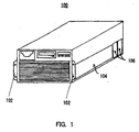
- FIG. 1 is a schematic perspective view of the electronic apparatus 100.
- the electronic device 100 is implemented as a rack-mount type UNIX server.
- the electronic device 100 is screwed on a rack (not shown) by a pair of attachment parts 102, and mounted with a printed board 110 shown in FIGS. 2A-2C in a housing 104.
- the housing 104 has a fan module 106, in which a built-in cooling fan rotates to generate the airflow and compulsorily cools a built-in heat sink.
- the printed board 110 includes a package (electronic component) 120, plural block plates (not shown), into which a memory card is to be inserted, and one or more connectors (not shown) for use with external units, such as a hard disc drive (“HDD”) and a LAN.
- the package 120 can use any one of a BGA, an LGA, and a PGA.
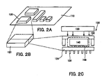
- FIG. 2A is a schematic perspective view of the printed board 110 mounted with the package 120 (which is a CPU package in an example) configured to house an LSI chip of this embodiment.
- FIG. 2B is a schematic perspective view of the package 120.
- FIG. 2C is a schematic sectional view of the package 120 taken along a dotted line shown in FIG. 2B .
- the package 120 houses the LSI chip 140. While the package 120 of this embodiment is a single chip type that is mounted with one LSI chip 140, but the present invention does not exclude a multi-chip type package.
- the package 120 has a substrate 124, on which the LSI chip 140 is mounted. Electrodes connectable to bumps of the LSI chip 140 are formed on a top surface of the substrate 124 as illustrated, and the bump and the electrode are electrically connected to each other. Since the substrate may have a dummy electrode that does not contribute to an electric connection, all the bumps and electrodes do not have to be electrically connected to each other. Plural input/output (I/O) pins 126 connectable to the printed board 110 are formed on a bottom surface of the substrate as illustrated.
- I/O input/output
- the package 120 contacts a heat spreader 130 through a top surface 122 of the package 120 as shown in FIG. 2C .
- the heat generated from the LSI chip 130 transmits to the heat spreader 130 via the package's top surface 122.
- the heat spreader 130 serves to transmit the heat from the LSI chip 130 to a heat sink (not shown), and is made of a material having high thermal conductivity, such as AIN and Cu.
- a thermal grease or thermal sheet having a high thermal conductivity may be filled in between the heat spreader and the LSI chip 130.
- a member such as a stiffener, may be interposed.
- the heat sink (not shown) has a base and many cooling fins.
- the base is a plate composed of a material having a high thermal conductivity, such as aluminum, copper, aluminum nitride, artificial diamond, and plastic, and joined with the heat spreader 130.
- the heat sink is manufactured by sheet metal working, aluminum die casting, or other processes, and if it is made of plastic, it may be formed, for example, by injection molding.
- the cooling fin has an arbitrary shape, such as a plate shape and a pin shape, to maintain a heat radiation area. An arrangement of the fins and the number of fins are arbitrary and each fin is made of a material having a high thermal conductivity.
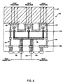
- FIG. 3 is a schematic enlarged sectional view of the LSI chip 140.
- the LSI chip 140 includes plural transistors 142, each of which is mounted on a corresponding one of connectors 143 on a substrate 141.
- signal wires are formed by multilayered wires.
- Each connector 143 is connected to one or more signal wires 144 including a power supply wire, and each signal wire 144 is connected to a bump 148 that serves as an LSI I/O terminal.
- the signal wire 144 is made of a metallic wire that constitutes a network that connects inputs and outputs of the transistor 142.
- the bumps 148 are connected to an external board via wires of the package 120, and the transistor 142 is electrically connected to the external board via the signal wires 144 and the bumps 148.
- the substrate 141 that serves as an LSI substrate contacts the heat spreader 130 via the top surface of the package 120 as illustrated.
- the LSI chip 140 further includes one or more heat radiation wire or dummy wires 146 that serve as heat radiation wires.
- the heat radiation wire 146 is made by an approach similar to the signal wire 144.
- the heat radiation wires 146 constitute a dedicated thermal conduction network independent of the electric transistor network.
- the heat radiation wires 146 are at least partially provided between wiring layers 145a and 145b of the signal wire 144, are electrically insulated from the transistor 142, and radiate heat from the transistor 142.
- the wiring layer 145a is the lowermost wiring layer nearest the transistor, the wiring layer 145b is the uppermost layer, and there can be plural wiring layers between them. Since the heat radiation wire 146 is provided in the wiring layer, the heat radiation efficiency is higher than that of the heat radiation structure that radiates the heat outside the LSI chip as in Japanese Patent Applications Nos. 2002-11902 , 2000-323525 , and 2003-17494 .
- the transistor 142 is insulated from the heat radiation wires 146.
- the heat radiation wire 146 is made of a metallic line, the transistor 142 is spaced from the heat radiation wire 146.
- the heat radiation wire 146 is an insulator, both can contact each other.
- the heat radiation wires 146 provided between the wiring layers 145a and 145b radiate heat from the transistors 142. Since the LSI chip has a new heat emission path as shown by an oblique arrow in FIG. 5 , the heat radiation efficiency is higher than that of the conventional LSI chip shown in FIG. 8 . This configuration can therefore protect the transistors 142 from thermal damages, and maintain their electric characteristics.
- the LSI chip 140 can use a Law-k interlayer film material and a higher operational frequency.
- the signal wires 144 and the heat radiation wires 146 are connected to different bumps 148.
- the bumps 148 serve as heat exhaust port. Use of the bumps 148 that are inherently provided in the LSI chip 140 can prevent the increased number of components and maintain the size of the chip 140.
- the heat radiation wire 146 is made of a metallic material having a high thermal conductivity, such as cupper and aluminum.
- the heat radiation wire 146 is made of the same material as that of the signal wire 144, the same machine can form both the signal wires 144 and the heat radiation wires 146 as dummy wires.
- the heat radiation wire 146 may be made of a dedicated material different from the signal wire 144.
- the heat radiation wire 146 may have the same diameter as that of the signal wire 146. It is conceivable to make a diameter of the heat radiation wire 146 greater than that of the signal wire 144 so as to enhance the heat radiation efficiency, but this configuration would increase the size of the chip 140. However, the present invention allows the diameter of the heat radiation wire 146 to be greater than the signal wire 144, when the large size of the chip 140 is permissible or when the enhanced heat radiation efficiency is highly required.
- the heat exhaust port of the heat radiation wire 146 is not limited to the bump 148.
- the heat radiation wire 146 may further include a heat radiation wire 146a that is connected to a heat conducting member 141a that perforates the substrate 141, as shown in FIG. 4 . Thereby, the heat from the heat radiation wire 146 is transmitted to the heat spreader 130.
- the heat conductor 141a is made of the above material having the high thermal conductivity.
- the heat radiation wire 146 may extend perpendicular to a lamination direction of the signal wires 144 and expose to the outside, like a heat radiation wire 146b.
- the package 110 may further include a member configured to radiate heat from the taken-out part of the heat radiation wire.
- the heat radiation member may use natural cooling, such as a heat sink, or compulsory cooling, such as a heat pipe and a cooling fan.
- the heat radiation wire 146 may have a meshed member 147 in the uppermost wiring layer 145b or a wiring layer near the uppermost wiring layer 145b.
- FIG. 6A is a schematic enlarged perspective view of the meshed member 147.
- the meshed member 147 has an effect of uniformly dispersing the locally generated heat in the LSI chip 140. As long as the heat dispersion effect is maintained, the mesh shape is not necessarily required.
- the heat radiation wire 146 includes a part 146c that is spaced from the transistor 142, and extends parallel to the surface of the transistor 142. Spacing from the transistor 142 can prevent the heat radiation wire 146 from deteriorating the electric characteristic of the transistor 142.
- a parallel arrangement to the surface of the transistor 142 rather than a perpendicular arrangement to the surface of the transistor 142 enables the heat radiation wire 146 to uniformly receive the heat from the transistor 142 in a direction in which the heat radiation wire 146c extends.
- the heat radiation wire 146c in the uppermost wiring layer 145a above the transistor absorbs the heat generated around the transistor 142, and transmits the heat to the uppermost wiring layer 145b.
- a connecting line 146d from the uppermost wiring layer 145a to the meshed member 147 can be sufficiently made with a minimum critical dimension of the technology to be used.
- a thickness of the upper mesh depends upon a mask design rule concerning connections with the bumps 148.
- the part 146c when the part 146c has a plate 146e parallel to the surface of the transistor 142, the part 146c can uniformly receive the heat from the whole surface of the transistor 142.
- the mesh structure permits the signal wires to pass through it, and a plate may be used instead of the mesh in an area that has no signal wires.
- the present invention is not limited to these embodiments and various variations and modifications may be made without departing from the scope of the present invention.
- the electronic apparatus of the present invention is not limited to the rack-mount type server, but is applicable to a bookshelf type.
- the electronic apparatus of the present invention is not limited to a server, but is applicable to a personal computer, a network device, a cellular phone, a PDA, and another peripheral.
- the present invention is applicable to an exoergic circuit element that does not serve as a CPU, such as a chipset.
- the present invention can provide an electronic device having better heat radiation efficiency, a package having the same, and an electronic apparatus.
- the present invention further discloses the following items:
Landscapes
- Cooling Or The Like Of Semiconductors Or Solid State Devices (AREA)
Abstract
Description
- The present invention relates generally to an electronic apparatus that houses a circuit element, such as an LSI, and more particularly to a heat radiation structure for the circuit element that generates heat when it is operating. The present invention is suitable, for example, for heat radiations for LSI chips in a wide variety of packages, such as a ball grid array ("BGA"), a land grid array ("LGA"), and a pin grid array ("PGA").
- Along with recently widespread, small and sophisticated electronic apparatuses, a supply of an electronic apparatus that realizes high density mounting is increasingly demanded. In order to meet this demand, a BGA package is conventionally proposed. In general, the BGA package is one type of a package that is soldered to a printed board (also referred to as a "system board" or a "motherboard"), and is mounted with an IC or an LSI that generally serves as a CPU. The BGA package realizes a narrow pitch and multiple pins (many leads), and provides a sophisticated electronic apparatus through a higher density package.
- As the CPU's performance improves, the heating value of the CPU increases and, in order to thermally protect the CPU, a cooling device called a heat sink is thermally connected to the CPU via a heat spreader. The heat sink includes cooling fins, stands close to the CPU, and radiates heat from the CPU through natural cooling.
-
FIG. 7 shows a schematic section of aconventional LSI chip 10 housed in a package. TheLSI chip 10 includestransistors 12, each of which serves as an exoergic circuit element, and is mounted on a corresponding one ofconnectors 14 on asubstrate 11. Theconnector 14 is connected to one or more signal wires (including a power supply wire) 16. Eachsignal wire 16 is connected to a corresponding one ofbumps 18. Thebump 18 is connected to an external board, and thetransistor 12 is electrically connected to the external board via thesignal wires 16 and thebumps 18. Thesubstrate 11 contacts a heat spreader (not shown) via a top surface of the package. Thus, theconventional LSI chip 10 radiates heat only from thesubstrate 11's surface side, as shown inFIG. 8 , and does not radiate the heat from thebumps 18 side. - Other prior art relating to the heat radiation include, for example, Patent Documents 1-3:
- Patent Document 1: Japanese Patent Application No.
2002-11902 - Patent Document 2: Japanese Patent Application No.
2000-323525 - Patent Document 3: Japanese Patent Application No.
2003-17494 - The heating value has recently increased with a higher operational frequency of the transistor and higher density mounting. In general, as the temperature of a CMOS transistor rises, the mobility of electrons (holes) in a channel lowers and the performance of the CMOS transistor degrades. On the other hand, the substrate is too thick to improve the heat radiation efficiency. In particular, in the SOI technology, the heat radiation by the self-heating substrate is insufficient. In addition, a Low-k interlayer film material, such as SiLK, which is used to reduce the wiring parasitic capacity, contains air bubbles in its inside, and exhibits poor heat conductions. As a result, as shown in
FIG. 8 , the heat exhausts near the transistor become insufficient. - Accordingly, it is an illustrative object of the present invention to provide an electronic device having better heat radiation efficiency, a package having the same, and an electronic apparatus.
- According to one aspect of the present invention an electronic device include a circuit element that transmits a signal to an external board and receives the signal from the external board, a signal wire that connects the external board to the circuit element, and a heat radiation wire that thermally contacts the circuit element, and radiates heat from the circuit element. This electronic device uses the heat radiation wire to protect the circuit element from thermal damages, and to maintain the electric characteristic. Therefore, this electronic device can use of a Low-k interlayer film material, and a higher operational frequency. The heat radiation wire may be electrically insulated from the circuit element. Thereby, the heat radiate wire can prevent degradations of the electric characteristic of the circuit element.
- The electronic device may further include a bump that is connectible to the external board, wherein the heat radiation wire is thermally connected to the bump. In this case, the bump serves as a thermal exhaust port. The electronic device may further include plural bumps that are connectible to the external board, wherein the signal wire and the heat radiation wire are connected to different bumps among the plural bumps. Use of different bumps prevents degradations of the electric characteristic of the circuit element. Use of the bump that is inherently provided on the chip does not increase the number of components, and maintains the size of the chip.
- The heat radiation wire may be made of a metallic material having a high thermal conductivity, such as cupper and aluminum. When the heat radiation wire is made of the same material as that of the signal wire, the same machine can form both the signal wires and the heat radiation wires as dummy wires. The heat radiation wire may have the same diameter as that of the signal wire. It is conceivable to make a diameter of the heat radiation wire greater than that of the signal wire so as to enhance the heat radiation efficiency, but this configuration would increase the size of the chip. However, the present invention allows the diameter of the heat radiation wire to be greater than the signal wire, when the large size of the chip is permissible or when the enhanced heat radiation efficiency is highly required.
- The heat radiation wire may have a part that is spaced from the circuit element and extends parallel to a surface of the circuit element. Spacing from the circuit element can prevent the heat radiation wire from deteriorating the electric characteristic of the circuit element. A parallel arrangement to the surface of the circuit element rather than a perpendicular arrangement to the surface of the circuit element enables the heat radiation wire to uniformly receive the heat from the circuit element in a direction in which the heat radiation wire extends.
- The electronic device may further include a dispersion member that is connected to the heat radiation wire, and disperses heat from the heat radiation wire. The dispersion member is, for example, a meshed member. The dispersion member can make the heat radiation efficiency uniform in the chip plane. The mesh structure permits the signal wires to pass through it, and a plate may be used instead of the mesh in an area that has no signal wires. The dispersion member may be formed in a wiring layer farthest from the circuit element among wiring layers of the signal wire. Thereby, the heat radiation efficiency in the final layer can be made uniform in the electronic device plane.
- The heat exhaust port for the heat radiation wire is not limited to the bump. For example, an electronic device may further include a substrate that is mounted with the circuit element, and radiates heat from the circuit element, and a heat conductor that perforates the substrate, and is connected to the heat radiation wire. Moreover, the heat radiation wire may extend perpendicular to a lamination direction of the signal wire, and expose to outside.
- A circuit package according to another aspect of the present invention includes an electronic device that includes a circuit element, and a heat radiation wire that thermally contacts and radiates heat from the circuit element, a substrate that is mounted with the circuit element, and electrically connected to the circuit element, and a pin provided onto the substrate and electrically connected to an external board. This circuit package can exhibit the operation of the above circuit device. The circuit package may further include a heat conductor that is thermally connected to the electronic device, and leads the heat that is generated from the electronic device to the outside. The heat conductor effectuates the heat exhausts. The heat conductor may use natural cooling, such as a heat sink, or compulsory cooling, such as a heat pipe and a cooling fan.
- An electronic apparatus according to still another aspect of the present invention includes an electronic circuit that includes a circuit element, a heat radiation wire that radiates heat generated from the circuit element, and a signal wire that is electrically connected to the circuit element, and a circuit board mounted with and electrically connected to the electronic circuit. This circuit package can exhibit the operation of the above circuit device.
- Other aspects of the present invention will become apparent from the following description and the attached drawings.
-
- [
FIG. 1 ] is a schematic perspective view of an electronic apparatus according to the present invention. - [
FIG. 2] FIG. 2A is a schematic perspective view of a printed board mounted with a package configured to house an LSI chip according to the present invention.FIG. 2B is a schematic perspective view of the package.FIG. 2C is a schematic sectional view of the package taken along a dotted line shown inFIG. 2B . - [
FIG. 3 ] is a schematic enlarged sectional view of the LSI chip shown inFIG. 2 . - [
FIG. 4 ] is a schematic enlarged sectional view of a variation of the LSI chip shown inFIG. 2 . - [
FIG. 5 ] is a schematic sectional view for explaining a heat radiation effect of the LSI chip shown inFIG. 3 . - [
FIG. 6] FIG. 6A is a schematic enlarged perspective view of a meshed member applicable to the LSI chip shown inFIG. 5 .FIG. 6B is a partial perspective view of a variation ofFIG. 6A . - [
FIG. 7 ] is a schematic enlarged sectional view of a conventional LSI chip. - [
FIG. 8 ] is a schematic sectional view for explaining the heat radiation effect of the LSI chip shown inFIG. 7 . - Referring now to the accompanying drawings, a description will be given of an
electronic apparatus 100 according to one embodiment of the present invention. Here,FIG. 1 is a schematic perspective view of theelectronic apparatus 100. As shown inFIG. 1 , theelectronic device 100 is implemented as a rack-mount type UNIX server. Theelectronic device 100 is screwed on a rack (not shown) by a pair ofattachment parts 102, and mounted with a printedboard 110 shown inFIGS. 2A-2C in ahousing 104. Thehousing 104 has afan module 106, in which a built-in cooling fan rotates to generate the airflow and compulsorily cools a built-in heat sink. - The printed
board 110 includes a package (electronic component) 120, plural block plates (not shown), into which a memory card is to be inserted, and one or more connectors (not shown) for use with external units, such as a hard disc drive ("HDD") and a LAN. Thepackage 120 can use any one of a BGA, an LGA, and a PGA. -
FIG. 2A is a schematic perspective view of the printedboard 110 mounted with the package 120 (which is a CPU package in an example) configured to house an LSI chip of this embodiment.FIG. 2B is a schematic perspective view of thepackage 120.FIG. 2C is a schematic sectional view of thepackage 120 taken along a dotted line shown inFIG. 2B . As shown inFIG. 2C , thepackage 120 houses theLSI chip 140. While thepackage 120 of this embodiment is a single chip type that is mounted with oneLSI chip 140, but the present invention does not exclude a multi-chip type package. - The
package 120 has asubstrate 124, on which theLSI chip 140 is mounted. Electrodes connectable to bumps of theLSI chip 140 are formed on a top surface of thesubstrate 124 as illustrated, and the bump and the electrode are electrically connected to each other. Since the substrate may have a dummy electrode that does not contribute to an electric connection, all the bumps and electrodes do not have to be electrically connected to each other. Plural input/output (I/O) pins 126 connectable to the printedboard 110 are formed on a bottom surface of the substrate as illustrated. - The
package 120 contacts aheat spreader 130 through atop surface 122 of thepackage 120 as shown inFIG. 2C . The heat generated from theLSI chip 130 transmits to theheat spreader 130 via the package'stop surface 122. Theheat spreader 130 serves to transmit the heat from theLSI chip 130 to a heat sink (not shown), and is made of a material having high thermal conductivity, such as AIN and Cu. A thermal grease or thermal sheet having a high thermal conductivity may be filled in between the heat spreader and theLSI chip 130. In compressing theheat spreader 130 against thepackage 120, a member, such as a stiffener, may be interposed. - The heat sink (not shown) has a base and many cooling fins. The base is a plate composed of a material having a high thermal conductivity, such as aluminum, copper, aluminum nitride, artificial diamond, and plastic, and joined with the
heat spreader 130. The heat sink is manufactured by sheet metal working, aluminum die casting, or other processes, and if it is made of plastic, it may be formed, for example, by injection molding. The cooling fin has an arbitrary shape, such as a plate shape and a pin shape, to maintain a heat radiation area. An arrangement of the fins and the number of fins are arbitrary and each fin is made of a material having a high thermal conductivity. -
FIG. 3 is a schematic enlarged sectional view of theLSI chip 140. TheLSI chip 140 includesplural transistors 142, each of which is mounted on a corresponding one ofconnectors 143 on asubstrate 141. In theLSI chip 140 shown inFIG. 3 , signal wires are formed by multilayered wires. Eachconnector 143 is connected to one ormore signal wires 144 including a power supply wire, and eachsignal wire 144 is connected to abump 148 that serves as an LSI I/O terminal. Thesignal wire 144 is made of a metallic wire that constitutes a network that connects inputs and outputs of thetransistor 142. Thebumps 148 are connected to an external board via wires of thepackage 120, and thetransistor 142 is electrically connected to the external board via thesignal wires 144 and thebumps 148. Thesubstrate 141 that serves as an LSI substrate contacts theheat spreader 130 via the top surface of thepackage 120 as illustrated. - The
LSI chip 140 further includes one or more heat radiation wire ordummy wires 146 that serve as heat radiation wires. Theheat radiation wire 146 is made by an approach similar to thesignal wire 144. Theheat radiation wires 146 constitute a dedicated thermal conduction network independent of the electric transistor network. Theheat radiation wires 146 are at least partially provided betweenwiring layers signal wire 144, are electrically insulated from thetransistor 142, and radiate heat from thetransistor 142. - In
FIG. 3 , thewiring layer 145a is the lowermost wiring layer nearest the transistor, thewiring layer 145b is the uppermost layer, and there can be plural wiring layers between them. Since theheat radiation wire 146 is provided in the wiring layer, the heat radiation efficiency is higher than that of the heat radiation structure that radiates the heat outside the LSI chip as in Japanese Patent Applications Nos.2002-11902 2000-323525 2003-17494 - In order to prevent degradations of the electric characteristic of the transistor, the
transistor 142 is insulated from theheat radiation wires 146. When theheat radiation wire 146 is made of a metallic line, thetransistor 142 is spaced from theheat radiation wire 146. When theheat radiation wire 146 is an insulator, both can contact each other. - In the
LSI chip 140, theheat radiation wires 146 provided between thewiring layers transistors 142. Since the LSI chip has a new heat emission path as shown by an oblique arrow inFIG. 5 , the heat radiation efficiency is higher than that of the conventional LSI chip shown inFIG. 8 . This configuration can therefore protect thetransistors 142 from thermal damages, and maintain their electric characteristics. TheLSI chip 140 can use a Law-k interlayer film material and a higher operational frequency. - The
signal wires 144 and theheat radiation wires 146 are connected todifferent bumps 148. In this case, thebumps 148 serve as heat exhaust port. Use of thebumps 148 that are inherently provided in theLSI chip 140 can prevent the increased number of components and maintain the size of thechip 140. - The
heat radiation wire 146 is made of a metallic material having a high thermal conductivity, such as cupper and aluminum. When theheat radiation wire 146 is made of the same material as that of thesignal wire 144, the same machine can form both thesignal wires 144 and theheat radiation wires 146 as dummy wires. Of course, theheat radiation wire 146 may be made of a dedicated material different from thesignal wire 144. - The
heat radiation wire 146 may have the same diameter as that of thesignal wire 146. It is conceivable to make a diameter of theheat radiation wire 146 greater than that of thesignal wire 144 so as to enhance the heat radiation efficiency, but this configuration would increase the size of thechip 140. However, the present invention allows the diameter of theheat radiation wire 146 to be greater than thesignal wire 144, when the large size of thechip 140 is permissible or when the enhanced heat radiation efficiency is highly required. - The heat exhaust port of the
heat radiation wire 146 is not limited to thebump 148. For example, theheat radiation wire 146 may further include a heat radiation wire 146a that is connected to aheat conducting member 141a that perforates thesubstrate 141, as shown inFIG. 4 . Thereby, the heat from theheat radiation wire 146 is transmitted to theheat spreader 130. Theheat conductor 141a is made of the above material having the high thermal conductivity. Moreover, theheat radiation wire 146 may extend perpendicular to a lamination direction of thesignal wires 144 and expose to the outside, like aheat radiation wire 146b. AlthoughFIG. 4 shows thesignal wire 144 and theheat radiation wire 146 on the same plane, thesignal wire 144 does not contact anyheat radiation wire 146a or 146b. Thus, theheat radiation wire 146 can be taken out from an arbitrary position of theLSI chip 140. Thepackage 110 may further include a member configured to radiate heat from the taken-out part of the heat radiation wire. The heat radiation member may use natural cooling, such as a heat sink, or compulsory cooling, such as a heat pipe and a cooling fan. - The
heat radiation wire 146 may have a meshedmember 147 in theuppermost wiring layer 145b or a wiring layer near theuppermost wiring layer 145b.FIG. 6A is a schematic enlarged perspective view of themeshed member 147. Themeshed member 147 has an effect of uniformly dispersing the locally generated heat in theLSI chip 140. As long as the heat dispersion effect is maintained, the mesh shape is not necessarily required. - As shown in
FIG. 6A , theheat radiation wire 146 includes apart 146c that is spaced from thetransistor 142, and extends parallel to the surface of thetransistor 142. Spacing from thetransistor 142 can prevent theheat radiation wire 146 from deteriorating the electric characteristic of thetransistor 142. A parallel arrangement to the surface of thetransistor 142 rather than a perpendicular arrangement to the surface of thetransistor 142 enables theheat radiation wire 146 to uniformly receive the heat from thetransistor 142 in a direction in which theheat radiation wire 146c extends. - As shown in
FIG. 6A , theheat radiation wire 146c in theuppermost wiring layer 145a above the transistor absorbs the heat generated around thetransistor 142, and transmits the heat to theuppermost wiring layer 145b. A connectingline 146d from theuppermost wiring layer 145a to themeshed member 147 can be sufficiently made with a minimum critical dimension of the technology to be used. A thickness of the upper mesh depends upon a mask design rule concerning connections with thebumps 148. - As shown in
FIG. 6B , when thepart 146c has a plate 146e parallel to the surface of thetransistor 142, thepart 146c can uniformly receive the heat from the whole surface of thetransistor 142. The mesh structure permits the signal wires to pass through it, and a plate may be used instead of the mesh in an area that has no signal wires. - Furthermore, the present invention is not limited to these embodiments and various variations and modifications may be made without departing from the scope of the present invention. For example, the electronic apparatus of the present invention is not limited to the rack-mount type server, but is applicable to a bookshelf type. In addition, the electronic apparatus of the present invention is not limited to a server, but is applicable to a personal computer, a network device, a cellular phone, a PDA, and another peripheral. The present invention is applicable to an exoergic circuit element that does not serve as a CPU, such as a chipset.
- The present invention can provide an electronic device having better heat radiation efficiency, a package having the same, and an electronic apparatus.
- The present invention further discloses the following items:
-
- (Appendix 1) An electronic device comprising: a circuit element that transmits a signal to an external board and receives the signal from the external board; a signal wire that connects the external board to the circuit element; and a heat radiation wire that thermally contacts the circuit element, and radiates heat from the circuit element. (1)
(Appendix 2) An electronic device according to appendix 1, wherein the heat radiation wire is electrically isolated from the circuit element. -
- (Appendix 3) An electronic device according to appendix 1, further comprising a bump that is connectible to the external board, wherein the heat radiation wire is thermally connected to the bump. (2)
- (Appendix 4) An electronic device according to appendix 2, further comprising plural bumps that are connectible to the external board, wherein the signal wire and the heat radiation wire are connected to different bumps among the plural bumps.
- (Appendix 5) An electronic device according to appendix 1,
- wherein the heat radiation wire has a part that is spaced from the circuit element and extends parallel to a surface of the circuit element. (3)
- (Appendix 6) An electronic device according to appendix 1, further comprising a dispersion member that is connected to the heat radiation wire, and disperses heat from the heat radiation wire. (4)
- (Appendix 7) An electronic device according to appendix 4, wherein the dispersion member is formed in a wiring layer farthest from the circuit element among wiring layers of the signal wire. (5)
- (Appendix 8) An electronic device according to appendix 1, further comprising: a substrate that is mounted with the circuit element, and radiates heat from the circuit element; and a heat conductor that perforates the substrate, and is connected to the heat radiation wire. (6)
- (Appendix 9) An electronic device according to appendix 1, wherein the heat radiation wire extends perpendicular to a lamination direction of the signal wire, and exposes to outside. (7)
- (Appendix 10) A circuit package comprising: an electronic device that includes a circuit element, and a heat radiation wire that thermally contacts and radiates heat from the circuit element; a substrate that is mounted with the circuit element, and electrically connected to the circuit element; and a pin provided onto the substrate and electrically connected to an external board. (8)
- (Appendix 11) A circuit package according to appendix 8, further comprising a heat conductor that is thermally connected to the electronic device, and leads the heat that is generated from the electronic device to the external board. (9)
- (Appendix 12) An electronic apparatus comprising: an electronic circuit that includes a circuit element, a heat radiation wire that radiates heat generated from the circuit element, and a signal wire that is electrically connected to the circuit element; and a circuit board mounted with and electrically connected to the electronic circuit.
Claims (10)
- An electronic device comprising:a circuit element that transmits a signal to an external board and receives the signal from the external board;a signal wire that connects the external board to the circuit element; anda heat radiation wire that thermally contacts the circuit element, and radiates heat from the circuit element.
- An electronic device according to claim 1, further comprising a bump that is connectible to the external board, wherein the heat radiation wire is thermally connected to the bump.
- An electronic device according to claim 1, wherein the heat radiation wire has a part that is spaced from the circuit element and extends parallel to a surface of the circuit element.
- An electronic device according to claim 1, further comprising a dispersion member that is connected to the heat radiation wire, and disperses heat from the heat radiation wire.
- An electronic device according to claim 4, wherein the dispersion member is formed in a wiring layer farthest from the circuit element among wiring layers of the signal wire.
- An electronic device according to claim 1, further comprising:a substrate that is mounted with the circuit element, and radiates heat from the circuit element; anda heat conductor that perforates the substrate, and is connected to the heat radiation wire.
- An electronic device according to claim 1, wherein the heat radiation wire extends perpendicular to a lamination direction of the signal wire, and exposes to outside.
- A circuit package comprising:an electronic device that includes a circuit element, and a heat radiation wire that thermally contacts and radiates heat from the circuit element;a substrate that is mounted with the circuit element, and electrically connected to the circuit element; anda pin provided onto the substrate and electrically connected to an external board.
- A circuit package according to claim 8, further comprising a heat conductor that is thermally connected to the electronic device, and leads the heat that is generated from the electronic device to outside.
- An electronic apparatus comprising:an electronic circuit that includes a circuit element, a heat radiation wire that radiates heat generated from the circuit element, and a signal wire that is electrically connected to the circuit element; anda circuit board mounted with and electrically connected to the electronic circuit.
Applications Claiming Priority (1)
| Application Number | Priority Date | Filing Date | Title |
|---|---|---|---|
| PCT/JP2005/021053 WO2007057952A1 (en) | 2005-11-16 | 2005-11-16 | Electronic element, package having same, and electronic device |
Publications (2)
| Publication Number | Publication Date |
|---|---|
| EP1950805A1 true EP1950805A1 (en) | 2008-07-30 |
| EP1950805A4 EP1950805A4 (en) | 2010-03-03 |
Family
ID=38048344
Family Applications (1)
| Application Number | Title | Priority Date | Filing Date |
|---|---|---|---|
| EP05806818A Withdrawn EP1950805A4 (en) | 2005-11-16 | 2005-11-16 | ELECTRONIC COMPONENT, CASE WITH THE SAME, AND ELECTRONIC DEVICE |
Country Status (4)
| Country | Link |
|---|---|
| US (1) | US7643302B2 (en) |
| EP (1) | EP1950805A4 (en) |
| JP (1) | JP5115200B2 (en) |
| WO (1) | WO2007057952A1 (en) |
Families Citing this family (5)
| Publication number | Priority date | Publication date | Assignee | Title |
|---|---|---|---|---|
| JP5512992B2 (en) * | 2009-03-27 | 2014-06-04 | 国立大学法人 鹿児島大学 | Heat sink integrated package and manufacturing method thereof |
| US9538633B2 (en) * | 2012-12-13 | 2017-01-03 | Nvidia Corporation | Passive cooling system integrated into a printed circuit board for cooling electronic components |
| WO2016067351A1 (en) * | 2014-10-28 | 2016-05-06 | 株式会社日立製作所 | Method for cooling storage device |
| US9832876B2 (en) * | 2014-12-18 | 2017-11-28 | Intel Corporation | CPU package substrates with removable memory mechanical interfaces |
| RU179613U1 (en) * | 2017-10-13 | 2018-05-21 | Акционерное общество "Ордена Трудового Красного Знамени научно-исследовательский институт автоматической аппаратуры им. академика В.С. Семенихина" (АО "НИИАА") | Portable secure electronic computing device with a resistive forced cooling system |
Family Cites Families (26)
| Publication number | Priority date | Publication date | Assignee | Title |
|---|---|---|---|---|
| JP3035965B2 (en) * | 1990-03-28 | 2000-04-24 | 日本電気株式会社 | Semiconductor device |
| JP3047986B2 (en) * | 1990-07-25 | 2000-06-05 | 株式会社日立製作所 | Semiconductor device |
| JP3375224B2 (en) * | 1995-02-03 | 2003-02-10 | 三菱電機株式会社 | Semiconductor device and manufacturing method thereof |
| FR2735648B1 (en) * | 1995-06-13 | 1997-07-11 | Bull Sa | COOLING METHOD OF AN INTEGRATED CIRCUIT MOUNTED IN A HOUSING |
| JPH11238734A (en) * | 1998-02-20 | 1999-08-31 | Nec Corp | Semiconductor integrated circuit |
| JP3309907B2 (en) * | 1999-04-20 | 2002-07-29 | 日本電気株式会社 | Semiconductor device and manufacturing method thereof |
| JP3446818B2 (en) | 1999-05-10 | 2003-09-16 | 日本電気株式会社 | Semiconductor device mounting structure and method of manufacturing the same |
| JP2000331835A (en) * | 1999-05-21 | 2000-11-30 | Taiyo Yuden Co Ltd | Multilayer electronic components and circuit modules |
| JP2002011902A (en) | 2000-06-27 | 2002-01-15 | Sharp Corp | Image forming device |
| TW462121B (en) * | 2000-09-19 | 2001-11-01 | Siliconware Precision Industries Co Ltd | Heat sink type ball grid array package |
| TW490820B (en) * | 2000-10-04 | 2002-06-11 | Advanced Semiconductor Eng | Heat dissipation enhanced ball grid array package |
| JP2002110902A (en) | 2000-10-04 | 2002-04-12 | Toshiba Corp | Semiconductor element and semiconductor device |
| US6867493B2 (en) * | 2000-11-15 | 2005-03-15 | Skyworks Solutions, Inc. | Structure and method for fabrication of a leadless multi-die carrier |
| US7161239B2 (en) * | 2000-12-22 | 2007-01-09 | Broadcom Corporation | Ball grid array package enhanced with a thermal and electrical connector |
| JP2003017494A (en) | 2001-07-04 | 2003-01-17 | Matsushita Electric Ind Co Ltd | Semiconductor device and method of manufacturing the same |
| US6552907B1 (en) * | 2001-10-11 | 2003-04-22 | Lsi Logic Corporation | BGA heat ball plate spreader, BGA to PCB plate interface |
| EP1351301B1 (en) * | 2002-04-03 | 2009-06-17 | Panasonic Corporation | Semiconductor built-in millimeter-wave band module |
| US6657311B1 (en) * | 2002-05-16 | 2003-12-02 | Texas Instruments Incorporated | Heat dissipating flip-chip ball grid array |
| JP2004071670A (en) * | 2002-08-02 | 2004-03-04 | Fuji Photo Film Co Ltd | IC package, connection structure, and electronic device |
| JP3976089B2 (en) | 2002-08-09 | 2007-09-12 | 株式会社リコー | Semiconductor integrated circuit device and manufacturing method thereof |
| US6657864B1 (en) * | 2002-12-16 | 2003-12-02 | International Business Machines Corporation | High density thermal solution for direct attach modules |
| US6753600B1 (en) * | 2003-01-28 | 2004-06-22 | Thin Film Module, Inc. | Structure of a substrate for a high density semiconductor package |
| JP4084737B2 (en) * | 2003-11-20 | 2008-04-30 | 松下電器産業株式会社 | Semiconductor device |
| US7345364B2 (en) * | 2004-02-04 | 2008-03-18 | Agere Systems Inc. | Structure and method for improved heat conduction for semiconductor devices |
| US7269017B2 (en) * | 2004-11-19 | 2007-09-11 | Delphi Technologies, Inc. | Thermal management of surface-mount circuit devices on laminate ceramic substrate |
| US7148554B2 (en) * | 2004-12-16 | 2006-12-12 | Delphi Technologies, Inc. | Discrete electronic component arrangement including anchoring, thermally conductive pad |
-
2005
- 2005-11-16 EP EP05806818A patent/EP1950805A4/en not_active Withdrawn
- 2005-11-16 JP JP2007545125A patent/JP5115200B2/en not_active Expired - Fee Related
- 2005-11-16 WO PCT/JP2005/021053 patent/WO2007057952A1/en not_active Ceased
-
2008
- 2008-05-15 US US12/121,444 patent/US7643302B2/en not_active Expired - Fee Related
Also Published As
| Publication number | Publication date |
|---|---|
| JP5115200B2 (en) | 2013-01-09 |
| US7643302B2 (en) | 2010-01-05 |
| WO2007057952A1 (en) | 2007-05-24 |
| JPWO2007057952A1 (en) | 2009-04-30 |
| EP1950805A4 (en) | 2010-03-03 |
| US20080218965A1 (en) | 2008-09-11 |
Similar Documents
| Publication | Publication Date | Title |
|---|---|---|
| US6816378B1 (en) | Stack up assembly | |
| US6943293B1 (en) | High power electronic package with enhanced cooling characteristics | |
| JP3834023B2 (en) | LSI package with interface module and heat sink used therefor | |
| CN107708286B (en) | Printed circuit board assembly | |
| US6711021B1 (en) | Systems and methods that use at least one component to remove the heat generated by at least one other component | |
| US7643302B2 (en) | Electronic device, package having the same, and electronic apparatus | |
| US6778398B2 (en) | Thermal-conductive substrate package | |
| US20050270749A1 (en) | Thermally improved placement of power-dissipating components onto a circuit board | |
| CN100550360C (en) | Device and system with bottom cooling and method of manufacture | |
| US9558311B2 (en) | Surface region selection for heat sink placement | |
| CN101228627B (en) | Electronic module assemblies, portable electronic communication devices and printed circuit boards with heat sinks | |
| US7438558B1 (en) | Three-dimensional stackable die configuration for an electronic circuit board | |
| CN223414077U (en) | Power module packaging structure and electronic equipment | |
| CN106469693A (en) | Assembling structure of high-power semiconductor and radiator | |
| CN204834602U (en) | Assembly structure of high-power semiconductor and heat sink | |
| JPH07106721A (en) | Printed circuit board and heat dissipation method thereof | |
| CN121218432A (en) | Cooling module of rear power supply system | |
| CN217544599U (en) | Integrated circuit packaging structure | |
| CN223680106U (en) | Double-sided heat dissipation power module | |
| CN100466895C (en) | Heat radiation structure | |
| JP2009295763A (en) | Semiconductor mounting device, and electronic apparatus | |
| JPH11121660A (en) | Semiconductor device and manufacturing method thereof | |
| CN209283570U (en) | A kind of multilayer circuit board radiator structure | |
| CN110707055A (en) | Chips, Electronic Devices | |
| CN108738367A (en) | Electronic module |
Legal Events
| Date | Code | Title | Description |
|---|---|---|---|
| PUAI | Public reference made under article 153(3) epc to a published international application that has entered the european phase |
Free format text: ORIGINAL CODE: 0009012 |
|
| 17P | Request for examination filed |
Effective date: 20080611 |
|
| AK | Designated contracting states |
Kind code of ref document: A1 Designated state(s): DE FR GB |
|
| RBV | Designated contracting states (corrected) |
Designated state(s): DE FR GB |
|
| A4 | Supplementary search report drawn up and despatched |
Effective date: 20100128 |
|
| DAX | Request for extension of the european patent (deleted) | ||
| 17Q | First examination report despatched |
Effective date: 20130212 |
|
| GRAP | Despatch of communication of intention to grant a patent |
Free format text: ORIGINAL CODE: EPIDOSNIGR1 |
|
| INTG | Intention to grant announced |
Effective date: 20161005 |
|
| STAA | Information on the status of an ep patent application or granted ep patent |
Free format text: STATUS: THE APPLICATION IS DEEMED TO BE WITHDRAWN |
|
| 18D | Application deemed to be withdrawn |
Effective date: 20170216 |