EP1950796A2 - Procede destine a reduire l'exces de bruit dans des dispositifs electroniques - Google Patents
Procede destine a reduire l'exces de bruit dans des dispositifs electroniques Download PDFInfo
- Publication number
- EP1950796A2 EP1950796A2 EP06841690A EP06841690A EP1950796A2 EP 1950796 A2 EP1950796 A2 EP 1950796A2 EP 06841690 A EP06841690 A EP 06841690A EP 06841690 A EP06841690 A EP 06841690A EP 1950796 A2 EP1950796 A2 EP 1950796A2
- Authority
- EP
- European Patent Office
- Prior art keywords
- devices
- screen
- epilayer
- excess noise
- noise
- Prior art date
- Legal status (The legal status is an assumption and is not a legal conclusion. Google has not performed a legal analysis and makes no representation as to the accuracy of the status listed.)
- Withdrawn
Links
Images
Classifications
-
- H—ELECTRICITY
- H10—SEMICONDUCTOR DEVICES; ELECTRIC SOLID-STATE DEVICES NOT OTHERWISE PROVIDED FOR
- H10D—INORGANIC ELECTRIC SEMICONDUCTOR DEVICES
- H10D62/00—Semiconductor bodies, or regions thereof, of devices having potential barriers
- H10D62/60—Impurity distributions or concentrations
-
- H—ELECTRICITY
- H10—SEMICONDUCTOR DEVICES; ELECTRIC SOLID-STATE DEVICES NOT OTHERWISE PROVIDED FOR
- H10P—GENERIC PROCESSES OR APPARATUS FOR THE MANUFACTURE OR TREATMENT OF DEVICES COVERED BY CLASS H10
- H10P90/00—Preparation of wafers not covered by a single main group of this subclass, e.g. wafer reinforcement
- H10P90/19—Preparing inhomogeneous wafers
- H10P90/1904—Preparing vertically inhomogeneous wafers
- H10P90/1906—Preparing SOI wafers
- H10P90/1914—Preparing SOI wafers using bonding
-
- H—ELECTRICITY
- H10—SEMICONDUCTOR DEVICES; ELECTRIC SOLID-STATE DEVICES NOT OTHERWISE PROVIDED FOR
- H10D—INORGANIC ELECTRIC SEMICONDUCTOR DEVICES
- H10D62/00—Semiconductor bodies, or regions thereof, of devices having potential barriers
- H10D62/10—Shapes, relative sizes or dispositions of the regions of the semiconductor bodies; Shapes of the semiconductor bodies
- H10D62/17—Semiconductor regions connected to electrodes not carrying current to be rectified, amplified or switched, e.g. channel regions
-
- H—ELECTRICITY
- H10—SEMICONDUCTOR DEVICES; ELECTRIC SOLID-STATE DEVICES NOT OTHERWISE PROVIDED FOR
- H10D—INORGANIC ELECTRIC SEMICONDUCTOR DEVICES
- H10D62/00—Semiconductor bodies, or regions thereof, of devices having potential barriers
- H10D62/10—Shapes, relative sizes or dispositions of the regions of the semiconductor bodies; Shapes of the semiconductor bodies
- H10D62/17—Semiconductor regions connected to electrodes not carrying current to be rectified, amplified or switched, e.g. channel regions
- H10D62/351—Substrate regions of field-effect devices
- H10D62/357—Substrate regions of field-effect devices of FETs
-
- H—ELECTRICITY
- H10—SEMICONDUCTOR DEVICES; ELECTRIC SOLID-STATE DEVICES NOT OTHERWISE PROVIDED FOR
- H10D—INORGANIC ELECTRIC SEMICONDUCTOR DEVICES
- H10D62/00—Semiconductor bodies, or regions thereof, of devices having potential barriers
- H10D62/10—Shapes, relative sizes or dispositions of the regions of the semiconductor bodies; Shapes of the semiconductor bodies
- H10D62/17—Semiconductor regions connected to electrodes not carrying current to be rectified, amplified or switched, e.g. channel regions
- H10D62/351—Substrate regions of field-effect devices
- H10D62/357—Substrate regions of field-effect devices of FETs
- H10D62/364—Substrate regions of field-effect devices of FETs of IGFETs
- H10D62/371—Inactive supplementary semiconductor regions, e.g. for preventing punch-through, improving capacity effect or leakage current
-
- H—ELECTRICITY
- H10—SEMICONDUCTOR DEVICES; ELECTRIC SOLID-STATE DEVICES NOT OTHERWISE PROVIDED FOR
- H10D—INORGANIC ELECTRIC SEMICONDUCTOR DEVICES
- H10D62/00—Semiconductor bodies, or regions thereof, of devices having potential barriers
- H10D62/10—Shapes, relative sizes or dispositions of the regions of the semiconductor bodies; Shapes of the semiconductor bodies
- H10D62/17—Semiconductor regions connected to electrodes not carrying current to be rectified, amplified or switched, e.g. channel regions
- H10D62/351—Substrate regions of field-effect devices
- H10D62/357—Substrate regions of field-effect devices of FETs
- H10D62/364—Substrate regions of field-effect devices of FETs of IGFETs
- H10D62/378—Contact regions to the substrate regions
-
- H—ELECTRICITY
- H10—SEMICONDUCTOR DEVICES; ELECTRIC SOLID-STATE DEVICES NOT OTHERWISE PROVIDED FOR
- H10D—INORGANIC ELECTRIC SEMICONDUCTOR DEVICES
- H10D84/00—Integrated devices formed in or on semiconductor substrates that comprise only semiconducting layers, e.g. on Si wafers or on GaAs-on-Si wafers
- H10D84/01—Manufacture or treatment
-
- H—ELECTRICITY
- H10—SEMICONDUCTOR DEVICES; ELECTRIC SOLID-STATE DEVICES NOT OTHERWISE PROVIDED FOR
- H10D—INORGANIC ELECTRIC SEMICONDUCTOR DEVICES
- H10D84/00—Integrated devices formed in or on semiconductor substrates that comprise only semiconducting layers, e.g. on Si wafers or on GaAs-on-Si wafers
- H10D84/01—Manufacture or treatment
- H10D84/0123—Integrating together multiple components covered by H10D12/00 or H10D30/00, e.g. integrating multiple IGBTs
- H10D84/0126—Integrating together multiple components covered by H10D12/00 or H10D30/00, e.g. integrating multiple IGBTs the components including insulated gates, e.g. IGFETs
- H10D84/0165—Integrating together multiple components covered by H10D12/00 or H10D30/00, e.g. integrating multiple IGBTs the components including insulated gates, e.g. IGFETs the components including complementary IGFETs, e.g. CMOS devices
- H10D84/0181—Manufacturing their gate insulating layers
-
- H—ELECTRICITY
- H10—SEMICONDUCTOR DEVICES; ELECTRIC SOLID-STATE DEVICES NOT OTHERWISE PROVIDED FOR
- H10D—INORGANIC ELECTRIC SEMICONDUCTOR DEVICES
- H10D84/00—Integrated devices formed in or on semiconductor substrates that comprise only semiconducting layers, e.g. on Si wafers or on GaAs-on-Si wafers
- H10D84/01—Manufacture or treatment
- H10D84/02—Manufacture or treatment characterised by using material-based technologies
- H10D84/03—Manufacture or treatment characterised by using material-based technologies using Group IV technology, e.g. silicon technology or silicon-carbide [SiC] technology
- H10D84/038—Manufacture or treatment characterised by using material-based technologies using Group IV technology, e.g. silicon technology or silicon-carbide [SiC] technology using silicon technology, e.g. SiGe
-
- H—ELECTRICITY
- H10—SEMICONDUCTOR DEVICES; ELECTRIC SOLID-STATE DEVICES NOT OTHERWISE PROVIDED FOR
- H10D—INORGANIC ELECTRIC SEMICONDUCTOR DEVICES
- H10D84/00—Integrated devices formed in or on semiconductor substrates that comprise only semiconducting layers, e.g. on Si wafers or on GaAs-on-Si wafers
- H10D84/01—Manufacture or treatment
- H10D84/02—Manufacture or treatment characterised by using material-based technologies
- H10D84/05—Manufacture or treatment characterised by using material-based technologies using Group III-V technology
-
- H—ELECTRICITY
- H10—SEMICONDUCTOR DEVICES; ELECTRIC SOLID-STATE DEVICES NOT OTHERWISE PROVIDED FOR
- H10W—GENERIC PACKAGES, INTERCONNECTIONS, CONNECTORS OR OTHER CONSTRUCTIONAL DETAILS OF DEVICES COVERED BY CLASS H10
- H10W10/00—Isolation regions in semiconductor bodies between components of integrated devices
-
- H—ELECTRICITY
- H10—SEMICONDUCTOR DEVICES; ELECTRIC SOLID-STATE DEVICES NOT OTHERWISE PROVIDED FOR
- H10W—GENERIC PACKAGES, INTERCONNECTIONS, CONNECTORS OR OTHER CONSTRUCTIONAL DETAILS OF DEVICES COVERED BY CLASS H10
- H10W10/00—Isolation regions in semiconductor bodies between components of integrated devices
- H10W10/01—Manufacture or treatment
Definitions
- the invention falls in the field of electrical devices and more specifically in the semiconductor-based devices widely used in microelectronics both as discrete as well as monolithically integrated devices. More specifically it pertains to the area of noise reduction techniques for low-frequency excess noise in devices.
- SI-GaAs substrates are widely used in Monolithic Microwave Integrated Circuits (MIMICs) due to the good isolation that they provide when the epilayer existing between devices is removed by etching for example.
- GaAs devices made on p-type GaAs substrates that would to have similar devices made from a high mobility n-type epilayer on the substrate and also would bear a similar isolation between devices at dc and low frequencies, fail to isolate them at microwave frequencies due to the capacitive coupling between the conducting substrate and the devices of the high mobility n-type layer on top. Therefore a way to reduce excess noise in GaAs devices on SI-GaAs substrates or on substrates giving a good isolation between devices it is highly desirable.
- Silicon Microelectronics also suffers from this ubiquitous excess noise found both as a 1/f noise spectrum over thermal noise at low frequencies as well as one or more Lorentzian noise spectra emerging over thermal noise in the same low-frequency region, that sets a limit to the low-frequency performances of sensors and amplifiers working at or near zero frequency (dc).
- dc near zero frequency
- the processing of [1] aims to reduce carrier traps in MOS (Metal-Oxide-Semiconductor) devices by using fluorine to reduce the number of carrier traps which are believed in [1] to be the origin of the low frequency excess noise in MOS devices.
- MOS Metal-Oxide-Semiconductor
- the inventive method is capable of reducing 1 / f noise of the MOS device thus providing high performance analog integrated circuits.
- the presence of fluorine reduces the number of traps in the gate dielectric that carriers can translocate to".
- This invention explained by a classical theory involving carrier traps and its reduction has a doubtless merit for the particular process protected by the patent [1], but technically it is completely apart from our invention.
- JFET and HFET Junction and Heterojunction Field-Effect Tansistors
- MESFET Metal gate FETs
- BJT Bipolar Junction Transistors
- BJT Heterojunction Bipolar Transistors
- This radical invention comes from a novel theory that I have published recently, showing how excess noise is a consequence of transversal currents to the epilayer where the devices are, a kind of currents that are reinforced by the own biasing of the devices, being this an unpublished idea to my knowledge.
- the theory behind this invention departs radically from currently used theories that try to explain excess noise as an effect due to carrier traps, carefully designed to produce something like a 1/f noise spectrum. To say it bluntly, my novel theory leaves aside such hypothetical carrier traps and shows that the excess noise comes from the undeniable parasitic devices and effects that have been overseen (or not considered as such parasitics) over the course of time, more than eighty years ago.
- thermodynamic screen under the devices and, derived from its electrical screen effect appears the use of Surrounding-Gate Field-Effect Transistors (FET) to have a low excess noise in devices and monolithic integrated circuits as Operational Amplifiers for example.
- FET Field-Effect Transistors
- present invention is based on an electrical origin of the excess noise in electrical devices that has not been considered in the years elapsed from the first observations of "flicker noise" by Johnson in 1925.
- This electrical origin was unknown to most scientist being not concerned about excess noise or accepting theories more or less sophisticated as those assigning excess noise to carrier traps, temperature fluctuations and similar phenomena taking place where the aforementioned excess noise appears.
- This kind of theories makes difficult the appearance of an electrical or technological solution to reduce excess noise in semiconductor devices, but considering the electrical origin and thermodynamical character of the excess noise offered by the theory that backs present invention, excess noise reduction becomes easy to carry out and at a low cost as compared to the performances that can be achieved, all being promising for the industrial exploitation of this invention.
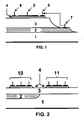
- the epitaxial GaAs layer (epilayer) used to make these devices is grown directly on the substrate or on a buffer layer grown previously that improves the morphology of further growth.
- a simple buffer designed for a purpose not proposed previously: to serve as the shield or thermodynamic screen described in this invention. Since the epilayer (4) of Figure (1 ) uses to be n-GaAs (due to the higher mobility for electrons than for holes), a low-barrier junction or low built-in contact potential (V bi ) junction will be formed between the substrate and the epilayer grown directly onto the semi-insulating substrate, whose reverse saturation currents are very high.
- the junction formed between the epilayer (4) and the screen-layer (2) is a p-n or p + -n GaAs junction having a much higher V bi than the V bi of the low-barrier junction that is formed by current technology and hence the much weaker transversal currents and the much lower excess noise existing in those devices protected by the thermodynamic screen formed by two layers: the screen layer (2) and the separating layer (3) of Figure 1 .
- this separating layer (3) is highly beneficial because besides its contribution to excess noise reduction, it is excellent for the high frequency performances of the devices. This is so because without the separating layer (3), the capacitance per unit area of the p + -n junction formed by the epilayer (4) grown directly onto the screen-layer (2) would be high, thus giving a high capacitance C DS between the drain (8) and source (6) of the FET of Figure 1 . This not only would increase the excess noise, but also it would degrade completely the high frequency performances of the FET.
- the growth of a separating layer of undoped GaAs (3) having 1 or 2 micron thickness will reduce C DS roughly 20 times, thus leaving a FET with good performances at high frequencies as well as with a low excess noise.
- the undoped GaAs layer (3) between the epilayer (4) and the screen-layer (2) does not change the high V bi character of the (p + -i-n) junction in regards to the transversal currents that will flow from the epilayer (4) to the screen-layer (2) and viceversa, thus leading to very low values for these transversal currents and its associated excess noise.
- the excess noise can be made null by the electrical connection that we have proposed by the dashed line of Figura 1, going from the ohmic contact (7) of the screen-layer (2) to the source (6) of the FET in the epilayer (4).
- a conducting p-GaAs substrate could be used that would act as screen-layer, thus requiring only the separating layer of undoped GaAs to reduce C DS in order to reduce excess noise in the devices together with an acceptable response at high frequencies.
- the separating layer (3) can be omitted, and moreover, the screen-layer (2) can be connected to the gate of the FET (5) of the epilayer (4), thus obtaining in this way a surrounding gate FET whose use as very low excess noise device also claims this invention due to the screen-layer function that layer (2) continues doing, although converted also in a part of the control gate of the FET, similar to its control gate (5).
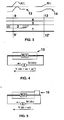
- Figure 2 shows an optimized application of the method of Figure 1 for its use with semi-insulating GaAs substrates that allows to have regions with isolated devices with very good performances at high frequencies (11) and other regions (10) with very low excess noise devices protected by this invention, dedicated to local oscillator and mixing functions, all in the same monolithic integrated circuit (IC).
- the layer structure could be obtained easily starting from a semi-insulating GaAs substrate (1) where an initial p-type implantation or diffusion (2) would be done in those regions where the low excess noise resistors and transistors will be fabricated (note that a resistor has the same structure of the FET whose cross section appears in Figure 1 , if the gate terminal (5) is not fabricated and the Source (6) and Drain (8) terminals are used as the resistor's terminals).
- an undoped GaAs layer of thickness close to 1 micron would be grown for the separating layer (3) that also would serve as a buffer to improve the crystalline quality of the GaAs growth that would be a very good one when the n-GaAs epilayer (4) was grown on top having a thickness of 0.3 microns and a doping level of 4 ⁇ 10 17 donors/cm 3 typically.
- FIG. 3 shows the band diagrams along a vertical direction in Figure 2 , for the case where the p-type screen-layer is crossed (cut 9-9') or not (cut 12-12').
- the corresponding band diagrams (13) and (14) along cuts 9-9' and 12-12' show why a thermodynamic screen is obtained that blocks or reduces the transversal currents from the epilayer (4) to the substrate (1) and viceversa.
- the band diagram (13) shows clearly the energy barrier that exists for these currents, a barrier that is absent in the band diagram (14) that is obtained without the aforementioned thermodynamic screen.
- the horizontal arrow in each band diagram (13) and (14) illustrates the carrier flux from the substrate to the epilayer, although an equal and opposed carrier flux would exist simultaneously thermal equilibrium (not shown for clarity purposes). It is apparent the additional barrier created by the p-type GaAs screen-layer (2) having in this example a p-doping opposed to the n-doping of the epilayer (4), but there are other methods, as those using band-engineering (heterojunctions), that also lead to create or to improve the barrier effect described in this example.
- Figure 4 shows the electrical cross section of many electrical devices having an inner conductive channel of a given resistance R ch surrounded by a neighbour conductor going in a roundabout way (14) to the former but isolated from it, that by Electrostatic laws forms a capacitor C surrounding the inner channel.
- the electrical geometry of Figure 4 appears in many electronic devices going from a simple coaxial cable to a more sophisticated conducting filaments as the microwires and nanowires under active research today.
- Figure 5 shows the simple connection (15) we have to do to reduce and remove in some cases the excess noise term (ac').
- This connection plays the same role that played in Figure 1 the connection done by a dashed line, which has inspired this one.
- Such role is to make null the thermodynamic noise of the surrounding capacitor C (its kT/C noise) that exists between the inner conductor and the outer conductor when they are left unconnected, as they appear in Figure 4 .
- connection (15) will remove the excess noise measured on the resistance R ch of the inner channel caused by currents transversal to the inner channel, that include both those currents due to the kT/C noise as well as the additional transversal currents induced by the voltage V dc appearing on R ch .
- the connection (15) can be done by a short circuit (that is a voltage generator of zero volts and very low impedance) but it will be also equally effective to reduce excess noise if it is done by means of a low impedance voltage generator also giving some dc or ac voltage signal.
- SGFET Surrounding Gate Field Effect Transistors
Landscapes
- Junction Field-Effect Transistors (AREA)
- Insulated Gate Type Field-Effect Transistor (AREA)
- Semiconductor Integrated Circuits (AREA)
Applications Claiming Priority (2)
| Application Number | Priority Date | Filing Date | Title |
|---|---|---|---|
| ES200502744A ES2274727B2 (es) | 2005-11-10 | 2005-11-10 | Metodo para reducir el exceso de ruido en dispositivos electronicos y en circuitos integrados monoliticos. |
| PCT/ES2006/000620 WO2007054595A2 (fr) | 2005-11-10 | 2006-11-10 | Procede destine a reduire l'exces de bruit dans des dispositifs electroniques |
Publications (1)
| Publication Number | Publication Date |
|---|---|
| EP1950796A2 true EP1950796A2 (fr) | 2008-07-30 |
Family
ID=38023619
Family Applications (1)
| Application Number | Title | Priority Date | Filing Date |
|---|---|---|---|
| EP06841690A Withdrawn EP1950796A2 (fr) | 2005-11-10 | 2006-11-10 | Procede destine a reduire l'exces de bruit dans des dispositifs electroniques |
Country Status (4)
| Country | Link |
|---|---|
| US (1) | US20090134435A1 (fr) |
| EP (1) | EP1950796A2 (fr) |
| ES (1) | ES2274727B2 (fr) |
| WO (1) | WO2007054595A2 (fr) |
Families Citing this family (1)
| Publication number | Priority date | Publication date | Assignee | Title |
|---|---|---|---|---|
| US20240204055A1 (en) * | 2022-12-17 | 2024-06-20 | Texas Instruments Incorporated | Screen layer integration in gallium nitride technology |
Family Cites Families (4)
| Publication number | Priority date | Publication date | Assignee | Title |
|---|---|---|---|---|
| JPH01243479A (ja) * | 1988-03-24 | 1989-09-28 | Nec Corp | ヘテロ接合電界効果トランジスタ |
| EP1037272A4 (fr) * | 1997-06-19 | 2004-07-28 | Asahi Chemical Ind | Substrat silicium sur isolant (soi) et procede d'elaboration, dispositif a semi-conducteurs et procede de fabrication |
| US6514825B1 (en) * | 2000-06-28 | 2003-02-04 | Conexant Systems, Inc. | Technique for reducing 1/f noise in MOSFETs |
| US7018880B2 (en) * | 2003-12-22 | 2006-03-28 | Texas Instruments Incorporated | Method for manufacturing a MOS transistor having reduced 1/f noise |
-
2005
- 2005-11-10 ES ES200502744A patent/ES2274727B2/es not_active Expired - Fee Related
-
2006
- 2006-11-10 WO PCT/ES2006/000620 patent/WO2007054595A2/fr not_active Ceased
- 2006-11-10 US US12/092,812 patent/US20090134435A1/en not_active Abandoned
- 2006-11-10 EP EP06841690A patent/EP1950796A2/fr not_active Withdrawn
Non-Patent Citations (1)
| Title |
|---|
| See references of WO2007054595A3 * |
Also Published As
| Publication number | Publication date |
|---|---|
| WO2007054595A2 (fr) | 2007-05-18 |
| US20090134435A1 (en) | 2009-05-28 |
| WO2007054595A3 (fr) | 2007-07-05 |
| ES2274727A1 (es) | 2007-05-16 |
| ES2274727B2 (es) | 2007-11-16 |
Similar Documents
| Publication | Publication Date | Title |
|---|---|---|
| KR101137196B1 (ko) | 하이퍼업럽트 접합을 갖는 접합 전계 효과 트랜지스터 | |
| US8330143B2 (en) | Semiconductor nanowire transistor | |
| US6355961B1 (en) | Structure and method for improved signal processing | |
| US5567629A (en) | Method of making transistor with oxygen implanted region | |
| US6524897B1 (en) | Semiconductor-on-insulator resistor-capacitor circuit | |
| US20140139282A1 (en) | Embedded JFETs for High Voltage Applications | |
| US7994550B2 (en) | Semiconductor structures having both elemental and compound semiconductor devices on a common substrate | |
| JPS6153861B2 (fr) | ||
| JP3325396B2 (ja) | 半導体集積回路 | |
| US7164160B2 (en) | Integrated circuit device with a vertical JFET | |
| JPH06349859A (ja) | 電界効果トランジスタ | |
| JP2003152184A (ja) | 絶縁性基板上の電界効果トランジスタおよびその集積回路 | |
| JPH0335536A (ja) | 電界効果型半導体装置 | |
| Mohtaram et al. | Physical analysis on the DC and RF operations of a novel SOI-MESFET with protruded gate and dual wells | |
| US5051808A (en) | Semiconductor device with low inductance of wirings connecting individual elements of the device | |
| JPH11168099A (ja) | 半導体装置 | |
| EP1950796A2 (fr) | Procede destine a reduire l'exces de bruit dans des dispositifs electroniques | |
| US20050194621A1 (en) | Double diffused vertical JFET | |
| JP3138182B2 (ja) | 電界効果トランジスタ | |
| JPS5889872A (ja) | 接合形電界効果半導体装置 | |
| JPS6228586B2 (fr) | ||
| US6137154A (en) | Bipolar transistor with increased early voltage | |
| JPS58122780A (ja) | 半導体装置 | |
| JPH055373B2 (fr) | ||
| Rieh | Semiconductor Technologies for THz Applications |
Legal Events
| Date | Code | Title | Description |
|---|---|---|---|
| PUAI | Public reference made under article 153(3) epc to a published international application that has entered the european phase |
Free format text: ORIGINAL CODE: 0009012 |
|
| 17P | Request for examination filed |
Effective date: 20080610 |
|
| AK | Designated contracting states |
Kind code of ref document: A2 Designated state(s): AT BE BG CH CY CZ DE DK EE ES FI FR GB GR HU IE IS IT LI LT LU LV MC NL PL PT RO SE SI SK TR |
|
| RIC1 | Information provided on ipc code assigned before grant |
Ipc: H01L 21/8238 20060101ALI20080911BHEP Ipc: H01L 21/336 20060101ALI20080911BHEP Ipc: H01L 21/20 20060101AFI20080911BHEP |
|
| STAA | Information on the status of an ep patent application or granted ep patent |
Free format text: STATUS: THE APPLICATION IS DEEMED TO BE WITHDRAWN |
|
| 18D | Application deemed to be withdrawn |
Effective date: 20110601 |