EP1949559B1 - Procede et systeme pour communications a pluralite d'antennes utilisant plusieurs modes de transmission, appareil et progiciel associes - Google Patents
Procede et systeme pour communications a pluralite d'antennes utilisant plusieurs modes de transmission, appareil et progiciel associes Download PDFInfo
- Publication number
- EP1949559B1 EP1949559B1 EP05799320A EP05799320A EP1949559B1 EP 1949559 B1 EP1949559 B1 EP 1949559B1 EP 05799320 A EP05799320 A EP 05799320A EP 05799320 A EP05799320 A EP 05799320A EP 1949559 B1 EP1949559 B1 EP 1949559B1
- Authority
- EP
- European Patent Office
- Prior art keywords
- replicas
- input
- signal
- diversity
- propagation paths
- Prior art date
- Legal status (The legal status is an assumption and is not a legal conclusion. Google has not performed a legal analysis and makes no representation as to the accuracy of the status listed.)
- Not-in-force
Links
Images


Classifications
-
- H—ELECTRICITY
- H04—ELECTRIC COMMUNICATION TECHNIQUE
- H04B—TRANSMISSION
- H04B7/00—Radio transmission systems, i.e. using radiation field
- H04B7/02—Diversity systems; Multi-antenna system, i.e. transmission or reception using multiple antennas
- H04B7/04—Diversity systems; Multi-antenna system, i.e. transmission or reception using multiple antennas using two or more spaced independent antennas
- H04B7/08—Diversity systems; Multi-antenna system, i.e. transmission or reception using multiple antennas using two or more spaced independent antennas at the receiving station
- H04B7/0891—Space-time diversity
- H04B7/0894—Space-time diversity using different delays between antennas
-
- H—ELECTRICITY
- H04—ELECTRIC COMMUNICATION TECHNIQUE
- H04B—TRANSMISSION
- H04B7/00—Radio transmission systems, i.e. using radiation field
- H04B7/02—Diversity systems; Multi-antenna system, i.e. transmission or reception using multiple antennas
- H04B7/04—Diversity systems; Multi-antenna system, i.e. transmission or reception using multiple antennas using two or more spaced independent antennas
- H04B7/06—Diversity systems; Multi-antenna system, i.e. transmission or reception using multiple antennas using two or more spaced independent antennas at the transmitting station
- H04B7/0613—Diversity systems; Multi-antenna system, i.e. transmission or reception using multiple antennas using two or more spaced independent antennas at the transmitting station using simultaneous transmission
- H04B7/0667—Diversity systems; Multi-antenna system, i.e. transmission or reception using multiple antennas using two or more spaced independent antennas at the transmitting station using simultaneous transmission of delayed versions of same signal
- H04B7/0671—Diversity systems; Multi-antenna system, i.e. transmission or reception using multiple antennas using two or more spaced independent antennas at the transmitting station using simultaneous transmission of delayed versions of same signal using different delays between antennas
Definitions
- the present invention relates to wireless communication systems.
- the invention was developed by paying specific attention to the possible application in radio transmitters and receivers.
- Radio transmitters and receivers used in systems that provide voice and data services by means of multiple transmission mode currently adopt different transmission modes characterized by different transmission parameters such as e.g. the channel coding rate.
- GPRS General Packet Radio Service
- EDGE Enhanced Data rates for Global Evolution
- HSDPA High Speed Downlink Packet Access
- LA Link Adaptation
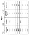
- FIG. 1 of the annexed drawing illustrates a set of transmission modes (MCS-1 to MCS-9) suitable for use in an EDGE system.
- Each mode listed in the left-hand column (Transmisson Mode or TM) is identified by the type of modulation (MOD - i.e. 8 PSK or GMSK) and the channel coding rate (i.e. the ratio of the "useful", payload bits to the total number of bits transmitted - right-hand column CR).
- the modes are listed in the figure in a decreasing order in terms of the maximum throughput (third column TM) in kbps, whereby MCS-9 and MCS-1 are the first and the last mode in the list, respectively. Since each mode has a different maximum data rate (expressed in bits per second) and robustness level (minimum signal-to noise ratio needed to activate the mode), the modes are optimal for use in different channel quality regions.
- the goal of link adaptation is thus always to ensure that the most efficient mode is used, over varying channel conditions, based on a mode selection criterion (maximum data rate, minimum transmit power, and so on).
- a mode selection criterion maximum data rate, minimum transmit power, and so on.
- MCS-1 the transmission mode denoted as MCS-1 ensures the highest protection of the transmitted information as it uses a low channel coding rate, of about 0.5, and a robust modulation scheme such the GMSK (Gaussian Minimum Shift Keying) modulation.
- GMSK Gausian Minimum Shift Keying
- the transmission mode denoted as MCS-5 provides a high level of protection of the transmitted information because it uses a channel coding rate of about 0.37 and uses the 8-PSK modulation scheme, which is less robust than the GMSK but is able to provide a throughput three times higher.
- These two transmission modes are selected under unfavourable channel conditions, as it may occur when the user is located at the cell edge.
- the transmission mode denoted as MCS-9 ensures the lowest protection of the information transmitted as it does not use any channel coding scheme and the coding rate is unitary. This transmission mode ensures the highest throughput and is used under very good channel conditions, as for example when the user is located near to the base station.
- HSDPA may be considered as a further example of a wireless system that uses multiple transmissions modes with different coding rates and modulations.
- HDSPA High Speed Downlink Packet Access
- 3GPP Release 5 specifications of UTRA includes a wide range of physical layer solutions able to increase user peak data rate and cell throughput, supporting a new downlink shared transport channel.
- the physical layer solutions include in particular multiple transmission modes characterized by different modulation and coding rates.
- HSDPA transmission modes (1 to 22 - column labelled TM) are listed in Figure 2 , for the User Equipment (UE) categories 1 to 6, with a number of spreading codes allocated to the High Speed Physical Downlink Shared CHannel (HS-PDSCH) between 1 and 5 (column labelled NC).
- Modulation may be either QPSK (for modes 1 to 15) or 16-QAM (for modes 16 to 22).
- the modes are listed in increasing order in terms of maximum throughput (MT) in kbps.
- MT maximum throughput
- CR channel coding rate varies from very low values of about 1/5 to rather high values of about 3/4.
- Antenna diversity is a technique that can be used to improve spectral efficiency and to reduce the negative effects of prolonged multi-path fading in wireless systems.
- two or more physically separated antennas space diversity
- one or more cross-polarized antenna polarization diversity
- space diversity space diversity
- polarization diversity cross-polarized antenna
- the physical separation between the antennas is limited due to size or environmental constraints and thus the signals can have a significant amplitude correlation.
- a significant signal correlation can also be present in the signals transmitted or received through cross polarized antennas, in particular when the vertical to horizontal polarization power ratio, also referred to as cross-polar discrimination (XPD), takes high values.
- XPD cross-polar discrimination
- the repeater is equipped with two receiving antennas for receiving a signal from a wireless terminal.
- the signal received from one of the antennas is subject to a fixed delay and is recombined at RF with the other received signal.
- the combined signal is subsequently transmitted to the base station by means of a third antenna.
- the fixed delay is chosen at least equal to two chip periods in order to enable the Rake receivers in the base station to resolve and coherently combine the two signals.
- the document WO-A-03/055097 describes a method for providing Phase Shift Transmit Diversity (PSTD) in a wireless communication system.
- a base station modulates the phase of a first signal with a reference signal to produce a first phase modulated signal. Further, the base station modulates the phase of a second signal with a different reference signal to produce a second phase modulated signal.
- the second phase shift is distinct from the first phase shift such that the second phase modulated signal is diverse relative to the first phase modulated signal. Accordingly, the base station transmits the first phase modulated signal via a first antenna and the second phase modulated signal via a second antenna to a plurality of mobile stations.
- EP 1 164 718 discloses a diversity type transmitter having a delay time control system for controlling the delay time of each of the plural transmission units so that the difference in delay time among the transmission units is within a permissible value range.
- PCT Applications PCT/EP2004/011204 and PCT/EP2005/010799 disclose antenna diversity techniques that improve radio link performance by reducing the temporal autocorrelation of the signals transmitted/received in low mobility scenarios and also minimize the cross-correlation among the signals received by the different antennas. These arrangements are applicable in wireless systems that have already been standardized, with minimal modifications on the deployed equipments and networks.
- DDD Dynamic Delay Diversity
- a time variable delay diversity introduces a time variable delay on the signals transmitted and/or received by the different antennas.
- the delay required to make the technique effective is significantly smaller when compared to other diversity techniques.
- the required delay varies between zero and the period of the RF (carrier) signal To.
- fixed DD fixed Delay Diversity
- the DDD technique also dispenses with certain problems that are intrinsic to Phase Shift Transmit Diversity (PSTD) techniques, such as e.g. high insertion loss and non-linearity of RF phase shifter devices.
- PSTD Phase Shift Transmit Diversity
- the object of the present invention is thus to provide an arrangement suitable for application in those communication systems that adapt to varying channel conditions by using different transmission modes.
- a specific object of the present invention is to provide an arrangement that, in the case of uncoded (e.g. EDGE mode MCS-9) or near-to-uncoded transmission, avoids that the distribution of the errors over the received data stream may cause an increase of the Block Error Rate (BLER) and thus a reduction of the user data rate.
- BLER Block Error Rate
- the invention also relates to a corresponding system, a related apparatus as well as a related computer program product, loadable in the memory of at least one computer and including software code portions for performing the steps of the method of the invention when the product is run on a computer.
- a computer program product is intended to be equivalent to reference to a computer-readable medium containing instructions for controlling a computer system to coordinate the performance of the method of the invention.
- Reference to "at least one computer” is evidently intended to highlight the possibility for the present invention to be implemented in a distributed/modular fashion.
- the claims are an integral part of the disclosure of the invention provided herein.
- a preferred embodiment of the invention is thus a method of diversity processing at least one signal propagated (i.e. transmitted and/or received) via at least two diversity antennas, the method including the steps of:
- the arrangement described herein thus comprises a new method and a related circuit for the application of a Dynamic Delay Diversity (DDD) technique.
- DDD Dynamic Delay Diversity
- the method and DDD circuit described herein are suitable for application in communication systems that adapt to varying channel conditions by using different transmission modes.
- the transmission modes are typically characterized by channel coding rates variable from 1 (unencoded transmission) to very low values (e.g. 1/3 or 1/5) obtained with powerful coding schemes.
- the arrangement described herein is applied to at least one signal transmitted by selectively using one of a plurality of transmission modes (e.g. MCS-1 to MCS-9; 1 to 22, as discussed previously) and said level imbalance is selected as a function of the transmission modes used, e.g. by using the level imbalance/difference giving the best results in connection with the transmission mode having the highest probability of being used.
- the level imbalance can be adaptively varied as a function of the current transmission mode used.
- GPRS e.g. GPRS
- EDGE e.g. UMTS
- HDR i.e. CDMA-2000
- EDGE EDGE
- HSDPA i.e. UMTS
- HDR i.e. CDMA-2000
- a preferred field of application of the arrangement described herein is in multi-carrier cell sites, in which the available carrier frequencies are divided among different transmission systems such GSM and GPRS/EDGE providing voice and packet data services respectively.
- the diversity arrangement described herein relies on the introduction of a time variant delay on the signals transmitted and/or received by the different antennas. Typically the delay is significantly smaller when compared to other diversity techniques. In general, if RF or IF signals modulated over a carrier are being processed according to the diversity arrangement described herein, the delay applied varies between zero and the period To of the carrier signal.
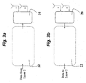
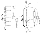
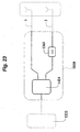
- the technique is realized by means of a diversity processor 10 (transmission or TX) that is connected at the output of a conventional transmitter 12, as shown in Figure 3a , or a diversity processor 20 (reception or RX) that is connected at the input of a conventional receiver 22 as shown in Figure 3b .
- a diversity processor 10 transmission or TX
- RX reception or RX
- digital signals (e.g. Layer 2 data in a mobile communication system - not shown as a whole) are transmitted ( figure 3a ) or received ( figure 3b ) via two diversity antennas 1 and 2.
- the transmitter 12 and the receiver 22 include otherwise conventional circuitry such as e.g. baseband processors, digital-to-analog (DAC) and analog-to-digital (ADC) converters, IF/RF transmitters/receivers, and so on.
- baseband processors e.g. baseband processors, digital-to-analog (DAC) and analog-to-digital (ADC) converters, IF/RF transmitters/receivers, and so on.
- DAC digital-to-analog
- ADC analog-to-digital converters
- IF/RF transmitters/receivers IF/RF transmitters/receivers
- DDD TX processors transmit diversity
- DDD RX processors receive diversity
- these TX or RX (or TX/RX, in the case of "reciprocal" embodiments) diversity processors will include various elements or components such as signal splitters, combiners, Time Variant Delay Lines (TVDL), Power Amplifiers (PA), Low Noise Amplifiers (LNA), etc.
- these elements are substantially the same in the various embodiments; these embodiments thus essentially differ in the number, type and way the various elementary blocks are combined to produce different structures of a diversity processor.
- the time varying delay required can be obtained using a delay line based on a waveguide or a microstrip device. Both devices, obtained using standard technologies as in commercial devices, are limited in power handling, where the limiting values are presently in the range of 33 - 35 dBm. This is not an issue for receive diversity applications, but might represent a limiting factor for transmission diversity applications: in several cases, in particular in the case of macro base station (for both 2G and 3G), this limiting value may not be compatible with the typical value of the transmitted power.
- the asymmetric DDD TX processors described here involve i.a. an asymmetric splitting of the power transmitted.
- the power level associated to the signal replica(s) subjected to the time varying delay may thus be reduced, which largely facilitates the implementation of several architectures proposed in the following by using commercial devices.
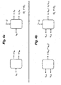
- the designation signal splitter - see figure 4a will apply to any device capable of splitting (i.e. dividing) an input signal S in in two parts or replicas.
- Such a splitter may either be:
- the designation signal combiner - see figure 4b - will apply to any device capable of combining (i.e. adding) two parts or replicas S in,1 , S in,2 of a given signal S in .
- Such a combiner may either be:
- splitters/dividers - both symmetric and asymmetric - also for RF/IF operation are conventional in the art and do not require to be described in detail here.
- a splitter implemented with passive components e.g. as a resistor voltage divider
- passive components will generally be reciprocal, in that it will act as a combiner for the signals that propagate in the opposite direction. This characteristic is exploited in the reciprocal DDD processors described in the following, which can be used simultaneously for transmission and reception.
- FIG. 4a and 4b highlight the possibility for an asymmetric splitter/combiner to include a control line C whereby the factors/weights ⁇ 1 and ⁇ 2 can be changed to correspondingly vary the difference/imbalance ⁇ .
- these factors/weights may be adjusted as a function of a transmission mode used e.g. by selecting the level imbalance/difference giving the best results in connection with the transmission mode having the highest probability of being used.
- these factors/weights may be adaptively varied during transmission as a function of the current transmission mode used.
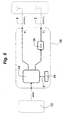
- a first architecture of a DDD TX processor 10 is shown in Figure 5 .
- This processor is suitable for application with conventional transmitters 12 that do not support any form of transmission antenna diversity.
- the conventional transmitter provides a single output signal.
- the DDD TX processor 10 includes an asymmetric splitter 14 that divides the input signal in two parts or replicas. The powers of the signals at the output of the asymmetric splitter are different.
- the power imbalance or difference thus created between the two signals to be transmitted via the diversity antennas 1 and 2 is a design parameter that allows the application of the DDD processor in wireless systems that use multiple transmission modes with different coding rates.
- the first signal with power P 1 is propagated (i.e. radiated) by the first antenna 1.
- the second signal with power P 2 is provided to a Time Variant Delay Line (TVDL) 16 that introduces a time variant delay ⁇ 1 (t) on the signal radiated by the second antenna 2.
- TVDL Time Variant Delay Line
- coefficients may be possibly varied via the line C. This may either be in the form of a "una tantum " trimming of the system or in the form of automatic adjustment under the control of a block 19 sensitive to the current transmission mode used (e.g. any of the modes MCS-1 to MCS-9 or 1 to 22 contemplated in figures 1 and 2 ).
- a power imbalance between the signals transmitted by the two antennas 1, 2 can also be obtained by resorting to the alternative arrangement illustrated in figure 6 , where the same reference numerals already appearing in figure 5 are used to denote identical/equivalent components to those already described.
- the splitter 14 is a symmetric splitter and two power amplifiers (PA) 14a and 14b with different gains G 1 and G 2 are inserted in the propagations paths of the two replicas of the signal produced by the splitter 14 towards the antennas 1, 2.
- PA power amplifier
- the symmetric splitter 14 provides in this case two output signals with the same power.
- the power imbalance or difference between the two signals to be transmitted via the diversity antennas 1 and 2 is thus produced by acting on the two gains G 1 and G 2 of the amplifiers 14a and 14b.
- the power imbalance or difference thus created allows the application of the DDD processor in wireless systems that use multiple transmission modes with different coding rates.
- a first signal with a first power level is propagated (i.e. radiated) by the first antenna 1
- the second signal with a second power level is processed (preferably before amplification at 14b) to a Time Variant Delay Line (TVDL) 16 that introduces a time variant delay ⁇ 1 ( t ) on the signal radiated by the second antenna 2.
- TVDL Time Variant Delay Line
- the amplitude coefficients ⁇ 1 , and ⁇ 2 of the formulas introduced in the foregoing are here dictated by the gains G 1 and G 2 of the amplifiers 14a and 14b. These gains/coefficients may again be possibly varied via respective control inputs C. This may be in the form of trimming of the system or in the form of automatic adjustment under the control of the block 19.
- the architecture illustrated in figure 6 has the advantage that the delay element 16 can be realized with low power handling components.
- the DDD TX processor architecture illustrated in Figure 6 is particularly adapted for communication networks that use Remote Radio Head (RRH) units.
- RRH Remote Radio Head
- a RRH is a compact unit that is mounted near the antenna and integrates several base station functions for transmission and reception.
- the transmission functions that are typically integrated in the RRH unit are digital to analog conversion (DAC), frequency up-conversion, digital pre-distortion and MCPA (Multi Carrier Power Amplifier).
- the receiving functions that are integrated in the RRH are the RF front-end, frequency down-conversion and analog to digital conversion (ADC).
- ADC analog to digital conversion
- the RRH unit is fed from the remainder of the base station with baseband (I/Q) signals via optical fibre cables.
- the interface between the RRH and the baseband modem is normally compliant with the Common Public Radio Interface (CPRI) standard or with the interface defined by the OBSAI (Open Base Station Standard Initiative) forum.
- CPRI Common Public Radio Interface
- OBSAI Open Base Station Standard Initiative
- FIG. 7a shows a first exemplary implementation of the time variable delay line 16 (and any other time variable delay line referred to in the rest of this description) in the form of a tapped delay line, namely as the cascade of elementary delay units.
- Each of such delay unit e.g. a transmission line stub
- T D 0.1 ns.
- the various tap points in the line come down to a RF switch 18.
- the switch is controlled by a delay control unit (DCU) making it possible to select a particular tap of the tapped delay line and therefore a given value of the delay introduced by the block. Changing the position of the switch 18 makes it possible to change the value of the delay.
- DCU delay control unit
- Two switches 181, 182 are controlled in a coordinated manner by the delay control unit (DCU) making it possible to select a particular delay element and therefore a given value of the delay introduced by the block. Changing the position of the switches 181, 182 makes it possible to change the value of the delay.
- DCU delay control unit
- the delay line/element As an alternative to varying the delay in discrete steps, as show in connection with the exemplary embodiments of Figure 7a and Figure 7b , in other possible implementations (not shown) of the delay line/element the delay is caused to vary continuously.
- a possible implementation of the delay line with continuous variation of the introduced delay can be found in the article " Time Delay Phase Shifter Controlled by Piezoelectric Transducer on Coplanar Waveguide", IEEE Microwave and Wireless Components Letters, Vol. 13, No. 1, pag. 19-20, January 2003 .
- the continuous delay line may be implemented by inserting on a coplanar waveguide a piezoelectric transducer whose perturbations vary the effective dielectric constant of the coplanar waveguide.
- the delay function ⁇ 1 ( t ), according to which the delay varies as a function of time, is not restricted to particular functions and can be a continuous function (e.g. linear, sinusoidal) or a discrete step function.
- An example of continuous delay function ⁇ 1 ( t ) is shown in Figure 8 , where T 0 is the carrier period and T DDD is the period of the delay function ⁇ 1 ( t ), which in the following will be designated the period of the DDD.
- T DDD is typically selected in the range between aprroximately one to tens of milliseconds.
- the coefficients a 1 and a 2 incorporate the amplitude coefficients ⁇ 1 , and ⁇ 2 , plus other gain factors (assumed to be identical for both signals) inherent in the transmission chain through which the "useful" signal x(t) is propagated, while ⁇ is representative of the (dynamic) time delay applied to the signal transmitted via the antenna 2.
- the second phasor r 2 (t), related to the signal transmitted by the antenna subject to variable delay, rotates with a frequency that is imposed by the period of the dynamic delay diversity DDD, as shown at the bottom of Figure 9 .
- the second phasor completes a rotation of 360° in a time interval equal to the period of the DDD (namely T DDD ).
- the combination of the two phasors at the receiving antenna A RX produces a resultant signal that fades at a faster rate than the signal without DDD, due to the alternation of constructive (phasors recombine in phase) and destructive combination (phasors recombine with opposite phases).
- the average amplitude ratio of the two phasors is directly proportional to the power imbalance ⁇ set at the transmitter in the DDD processor. As a consequence, the amplitude depth of the fades induced by the DDD can be progressively reduced by means of the power imbalance.
- the alternation of constructive and destructive combining reduces the length of the error bursts and thus improves the effectiveness of the transmission modes that use channel coding.
- the DDD technique thus affects the error statistics at the input of the channel decoder by making the error distribution more uniform over the received data stream (i.e. the error statistic becomes less bursty).
- the effectiveness of the channel decoding algorithms is then improved with a consequent reduction of the BLER after the decoding operation.
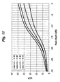
- FIG. 10 The effect of the DDD technique is shown in the diagrams of figure 10 .
- these diagrams provide a measure of the received signal power (ordinate scale) as a function of time (abscissa scale) in a system without DDD (diagram I) and in systems that use a DDD processor 10 at the transmitter (diagrams II and III).
- Figure 10 shows that the amplitude depth of the fades caused by the DDD is reduced by transmitting two signals with different powers.
- a lower amplitude depth of the induced fades reduces the probability that a block of unencoded bits is received with errors and therefore avoids any BLER degradation for the unencoded transmission modes.
- a second remarkable advantage of the unbalanced configuration is the simplification of the time variable delay line design, since the power associated to the second antenna can be significantly reduced.
- the effect of the power imbalance can be measured by means of a parameter that characterizes the fade occurrence on the received signal.
- This parameter is the fade rate or Level Crossing Rate (LCR).
- LCR is dependent on the environment characteristics (e.g. position and structure of the scattering objects) and on the relative speed between transmitter and receiver.
- the natural value of LCR in a given environment e.g. indoor
- LCR can be finely tuned by properly selecting the power imbalance ⁇ (line/input C of figures 5 and 6 ) of the DDD processor in order to get optimal link performance with systems that use multiple transmission modes.
- LCR is defined as the average rate at which the received signal envelope crosses a specified amplitude threshold A in a positive direction.
- the LCR is measured in number of fades per second, where the term fade means that the envelope crosses the threshold A.
- fade means that the envelope crosses the threshold A.
- CDMA systems engineering handbook J. Lee, L. Miller, pag. 256-262 .
- ⁇ is the fade-depth parameter defined as the ratio between the signal envelope threshold A and the local RMS (Root Mean Square) signal level
- ⁇ A A rms
- the LCR can be evaluated by simulation as shown in Figure 11 , where the LCR (ordinate scale) is given as a function of the fade depth parameter 10 ⁇ log 10 ( ⁇ 2 ) - abscissa scale, referred to the received power in decibel.
- the results indicate that the LCR reduces as the power imbalance increases (0dB, 3dB, 6dB, 9dB).
- a lower LCR corresponds to a lower amplitude depth of the induced fades and that reduces the probability that a block of uncoded bits is received with errors. With an accurate choice of the power imbalance is then possible to avoid the BLER degradation for the uncoded transmission modes.
- the application of the DDD processor in systems that use multiple transmission modes with different coding rates requires an accurate optimisation of the DDD parameters.
- the experimental measurements have shown that optimum link performance can be obtained with a period of the DDD of the same order of the interleaving period used in the communication system. This choice maximizes the effectiveness of channel coding and therefore the link performance gain for the transmission modes that use channel coding (indicatively with rates r ⁇ 1/2).
- the power imbalance ⁇ is instead optimised by considering the uncoded transmission modes or the transmission modes with the highest coding rates.
- the diagrams of Figures 12 , 13 and 14 provide some experimental measurement results obtained with an EDGE test-bed and using the DDD TX processor of figure 5 .
- the figures show the effect of the power imbalance on the link performance.
- the link performance is given in terms of BLER (ordinate scale) after channel decoding as a function of C/I (Signal to Interference plus Noise Ratio - abscissa scale) for the MCS-1, MCS-5 and MCS-9 transmission mode, respectively.
- the period of the DDD is set equal to 36 ms as it provides a good performance gain for the coded transmission modes, which use in the physical layer a block interleaving of 20 ms.
- a C/I gain of about 0.8 and 1 dB is measured for the MCS-1 and MCS-5 transmission modes at a target BLER of 10%, with respect to a system without DDD.
- Performance of the transmission mode MCS-9 with a power imbalance of 6 dB is the same of the conventional system without DDD, for a target BLER of 30%.
- the BLER targets of 10% and 30% considered are normally taken as reference working points in the deployment of the EDGE networks.
- the application of the DDD technique with power imbalance thus improves the overall spectral efficiency of the wireless communication system, even when multiple transmission modes with different coding rates are used.
- the degree of imbalance ⁇ will be increased as a function of the channel coding rate, which means that higher imbalance values (e.g. 6 dB) will be used for uncoded (e.g. HCS-9) or near-to-uncoded modes, so that the value of imbalance will approximately be proportional to the coding rate.
- the level imbalance value ⁇ is selected as a function of the transmission mode by selecting increasing (i.e. higher) level imbalance values for increasing (i.e. higher) coding rates.
- the specific values for ⁇ can be properly identified via numerical simulation or experimental testing.
- a preferred common feature to the various embodiments described herein lies in that, as the at least two signal replicas considered have respectively higher and lower power levels (i.e. the power level of the first replica is higher than the power level of the second replica, so that the power level of the second replica is lower than the power level of the first replica), the DDD arrangement described herein provides for the time variable delay being preferably applied to the replica having a lower power level. As indicated this is advantageous as it facilitates the use of low power handling components for the delay element(s).
- the DDD technique can be also used at the receiver side to improve the radio link performance of wireless systems even if not designed to support the receiver diversity.
- a conventional receiver 22 is equipped with a single radio chain and thus only one RF signal can be demodulated.
- the DDD RX processor 20 is an add-on RF module connected between the receiving antennas 1, 2 and the conventional receiver 22.
- the processor 20 includes an asymmetric combiner 24 and a time variant delay line 26.
- the signal received from the first antenna 1 is provided to the first input of the asymmetric combiner 24 while a second antenna 2 is added and this received signal is subject to the time variant delay 26 and then provided to the second input of the combiner.
- the combined signal is then provided to the conventional receiver 22 for the subsequent demodulation.
- the DDD RX processor 20 can also be realized according to the second architecture shown in Figure 16 .
- the signals received from the antennas 1, 2 are amplified by two Low Noise Amplifiers (LNAs) 24a and 24b with different gains G 1 and G 2 .
- the signal received from the first antenna 1 is provided to a symmetric RF combiner 24 while the signal from the second antenna 2 is subject to the time variant delay. After the insertion of the delay 26, the second signal is then provided to the other input of the symmetric combiner.
- the symmetric combiner adds the two input signals maintaining the power imbalance ⁇ of the signals at its inputs.
- the gains G 1 and G 2 of the LNAs 24a and 24b are set in order to obtain the desired power imbalance between the received signals prior to the RF combination.
- the effect of the power imbalance, in the case of the DDD technique is applied at the receiver side, is similar to that described in connection with figure 9 with reference to transmission of a single frequency component.
- the signals received at the antennas may be represented as two phasors, whose amplitude and phase change according to the channel characteristic. In low mobility environments these variations can be very slow thus causing prolonged signal fades.
- the insertion of the time variant delay on one of the received signals and the subsequent combination cause the alternation of constructive and destructive combining, which reduces the length of the error bursts and thus improves the effectiveness of the transmission modes that use channel coding.
- the alternation of constructive and destructive combining may negatively affect the Block Error Rate of the uncoded transmission modes.
- the DDD processors can be also applied to improve the performance of conventional transmitters and receivers that support some kind of transmission or receive antenna diversity.
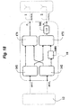
- FIG. 17 A block diagram of such a DDD TX processor is shown in Figure 17 .
- the signals INPUT 1 , INPUT 2 at the outputs of the conventional transmitter 12 feed two asymmetric splitters 141, 142. Each splitter divides the input signal in two replicas with different powers. Two of the four signals obtained after RF splitting are directly recombined in a first (symmetric) combiner 171, while the other two signals are subject to time variant delays in two delay elements 161 and 162 and then recombined in a second (symmetric) combiner 172. The signals after recombination feed the transmitting antennas 1, 2.
- the power asymmetry of the splitters is designed in order to obtain the desired imbalance ⁇ (see equation 1) between the powers P 1 and P 2 radiated by the two antennas 1, 2.
- ⁇ the desired imbalance between the powers P 1 and P 2 radiated by the two antennas 1, 2.
- ⁇ 1 and ⁇ 2 are the amplitude coefficients introduced by the first asymmetric splitter
- ⁇ 3 and ⁇ 4 are the amplitude coefficients introduced by the second asymmetric splitter.
- the arrangement illustrated in figure 17 corresponds to a specific, simplified implementation of a more general layout where time variable delay lines are associated to all of the four signal propagation paths that connect the inputs INPUT 1 and INPUT 2 to the antennas 1 and 2 via the splitters 141, 142 and the combiners 171, 172.
- the DDD TX processor 10 works as a signal decorrelator by providing two output signals that have a lower cross-correlation coefficient than the cross-correlation coefficient of the two input signals INPUT 1 and INPUT 2 .
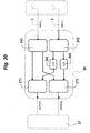
- the structure of the DDD TX processor of figure 17 can be simplified as illustrated in figure 18 .
- the two time variant delay lines 161, 162 of figure 17 are replaced by:
- the asymmetric/imbalanced arrangements of DDD TX processors of figures 17 and 18 can be also implemented by using symmetric splitters 141, 142 and cascading to the combiners 171, 172 two power amplifiers with different gains G 1 and G 2 .
- Figure 19 shows two such power amplifiers 14a, 14b with different gains G 1 and G 2 inserted prior to the antennas 1, 2 within the processor layout illustrated in figure 18 (the extension to the processor layout of figure 17 is straightforward and is not illustrated in detail).
- the gains of the power amplifiers 14a, 14b are determined in order to obtain the desired transmission power imbalance ⁇ .
- This architecture has the advantage that the DDD processor can be realized with low power components.
- the application of this architecture is suitable for communication networks that use Remote Radio Head (RRH) units.
- RRH Remote Radio Head
- the same DDD processor concept can be also employed at the receiver side in order to improve the performance of conventional receivers that support antenna diversity.
- the DDD RX processor is inserted between the antenna subsystem and the two RF inputs of a conventional receiver 22.
- a first architecture of such a DDD RX processor 20 is shown in Figure 20 .
- the received signals at the antennas are provided to two splitters 241, 242.
- Each splitter divides the input signal in two replicas with the same power.
- Two of the four signals obtained after RF splitting are directly recombined by means of an asymmetric combiner 271.
- the other two signals are subject to time variant delays 261, 262 and then asymmetrically recombined in a combiner 272.
- the signals after recombination then feed the conventional receiver.
- the asymmetry of the combiners 271, 272 is designed in order to obtain the desired imbalance ⁇ between the powers of the recombined signals.
- the arrangement illustrated in figure 20 corresponds to a specific, simplified implementation of a more general layout where time variable delay lines are associated to all of the four signal propagation paths that connect the antennas 1 and 2 to the outputs OUTPUT 1 and OUTPUT 2 via the splitters 241, 242 and the combiners 271, 272.
- the DDD RX processor operates as a signal decorrelator by providing two output signals that have a lower cross-correlation coefficient than the cross-correlation coefficient of the two input signals.
- the processor of Figure 20 can be simplified as illustrated in figure 21 .
- the two time variant delay lines 261, 262 of figure 20 are replaced by:
- the asymmetric/imbalanced arrangements of DDD RX processors of figures 20 and 21 can be also implemented by using symmetric combiners 271, 272 and placing upstream of the splitters 241, 242 two low noise amplifiers (LNAs) with different gains G 1 and G 2 .
- LNAs low noise amplifiers
- Figure 22 shows the arrangement resulting from the use of two such amplifiers 24a, 24b inserted at the outputs of the receiving antennas 1, 2.
- two symmetric combiners 271, 272 are used, while the gains of the LNAs 24a, 24b are designed in order to obtain the desired imbalance between the powers of the recombined signals.
- the application of this architecture (which can be applied also to the receiver layout of figure 20 ) is suitable for communication networks that use Remote Radio Head (RRH) units.
- RRH Remote Radio Head
- the DDD processors described up to now are unidirectional devices that can be used separately for transmission (TX) or reception (RX). Comparison of e.g. the architectures of Figure 5 (DDD TX processor) and Figure 15 (DDD RX processor) shows that the two circuits are inherently symmetrical.
- Figure 23 and figure 24 show the architectures of DDD TX/RX processors 1020 realized with reciprocal components that can be used simultaneously for transmission and reception.
- the separation of transmit and receive paths is realized within the transceiver by means of duplexer elements.
- the "transceiver" block 1222 in Figure 23 and 24 represents a unit that includes the functionalities of both the conventional transmitter and conventional receiver as shown in figures 3a and 3b , respectively.
- the block 1424 of figure 23 is a reciprocal module adapted to operate as an asymmetric splitter on the signal being transmitted from the TX section of the transceiver 1222 via the antennas 1, 2 and as an asymmetric combiner on the signals being received via the antennas 1, 2 and forwarded to the RX section of the transceiver 1222.
- the system of figure 24 thus includes:
- first splitters and the first combiners are in fact comprised of a first pair of reciprocal elements 14241, 14242.
- second splitters and the second combiners are in fact comprised of a second pair of reciprocal elements 17271, 17272.
- the arrangement illustrated in figure 24 can be alternatively implemented by using two (reciprocal) time variable delay elements playing the role of the transmission delay elements 161, 162 of figure 17 and the reception delay elements 261, 262 of figure 20 .
- the location of the power and low-noise amplifiers described and shown in connection with several embodiments disclosed in the foregoing represents the presently preferred design choice, but is in no way mandatory; the skilled designer may in fact easily devise different equivalent arrangements for these power and low-noise amplifiers while preserving their function of producing the power imbalance/difference underlying operation of the invention.
- DDD processors previously described can be combined in order to obtain different system architectures, where the DDD processing is introduced both in transmission and reception.
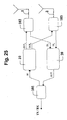
- figure 25 shows a first system architecture based on non-reciprocal DDD transmit and receive processors 10, 20.
- This architecture is suitable for conventional transceivers that do not support any form of transmit and receive antenna diversity.
- the internal structures of the DDD TX and RX processors 10, 20 can be e.g. those disclosed in the Figures 5 and 6 or Figures 15 and 16 for the TX and RX parts, respectively.
- a first duplexer element 101 separates the transmission and reception paths on the TX/RX side, and the separation between transmit and receive paths at the antennas 1, 2 is obtained by means of two further duplexer elements 102, 103.
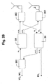
- Figure 26 illustrates another system architecture, realized with non-reciprocal processors, that is suitable for conventional transceivers that support only receive antenna diversity.
- the first duplexer element 101 here separates the transmission and reception paths TX 1 /RX 1 at the port supporting the single transmission channel and one of the diversity reception channels, and the separation between transmit and receive paths at the antennas 1, 2 is again obtained by means of two further duplexer elements 102, 103.
- the DDD TX processor 10 can be implemented e.g. according to any of the structures shown in Figure 5 or 6
- the DDD RX processor 20 can be implemented e.g. according to any of the schemes described in figures 20 , 21 or 22 .
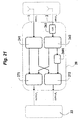
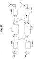
- FIG 27 illustrates still another system architecture, realized with non-reciprocal processors, which is suitable for conventional transceivers that support both transmit and receive antenna diversity.
- Two first duplexer elements 1011 and 1012 here separate the transmission and reception paths TX 1 /RX 1 and TX 2 /RX 2 at the two ports supporting the diversity transmission and reception channels. The separation between transmit and receive paths at the antennas 1, 2 is again obtained by means of two further duplexer elements 102, 103.
- the DDD TX processor 10 can be implemented e.g. according to any of the structures shown in figures 17 , 18 or 19
- the DDD RX processor can be implemented e.g. according to any of the schemes described in figure 20 , 21 or 22 .
- RF radiofrequency
- IF intermediate frequency
Claims (16)
- Procédé de traitement de diversité d'au moins un signal (INPUT ; INPUT1 ; INPUT2) propagé via au moins deux antennes à diversité (1, 2), le procédé comprenant l'étape consistant à propager au moins deux répliques dudit au moins un signal (INPUT ; INPUT1 ; INPUT2) sur des chemins de propagation respectifs couplés auxdites au moins deux antennes à diversité (1, 2), par laquelle quoi lesdites répliques sont propagées via des antennes différentes (1, 2) ;
caractérisé en ce qu'il comprend en outre les étapes consistant à :- soumettre au moins une desdites répliques à un retard variable dans le temps (16 ; 161, 162 ; 161, 1601 ; 1261 ; 26 ; 261, 262 ; 261, 2601 ; 1261) ; et- régler (14 ; 14, 14a, 14b ; 141, 142 ; 1424 ; 24 ; 24, 24a, 24b ; 241, 242 ; 271, 272 ; 14241, 14242) les niveaux de puissance desdites au moins deux répliques pour produire un déséquilibre de niveau (Δ) entre eux. - Procédé selon la revendication 1, caractérisé en ce que lesdites au moins deux répliques comprennent des répliques ayant respectivement des niveaux de puissance supérieur et inférieur, et en ce que le procédé comprend l'étape consistant à soumettre audit retard variable dans le temps (16 ; 161, 162 ; 161, 1601 ; 1261 ; 26 ; 261, 262 ; 261, 2601 ; 1261) ladite réplique ayant un niveau de puissance inférieur.
- Procédé selon l'une ou l'autre des revendication 1 ou 2, caractérisé en ce qu'il comprend l'étape consistant à sélectionner ledit déséquilibre de niveau (Δ) dans la plage de 3 à 10 dB.
- Procédé selon l'une quelconque des revendications 1 à 3, caractérisé en ce qu'il comprend les étapes consistant à :- utiliser sélectivement un parmi pluralité de modes de transmission (MCS-1 à MCS-9 ; 1 à 22) pour ledit au moins un signal ; et- sélectionner ledit déséquilibre de niveau (Δ) en fonction du mode de transmission utilisé.
- Procédé selon la revendication 4, caractérisé en ce que ladite pluralité de modes de transmission (MCS-1 à MCS-9 ; 1 à 22) a des débits de codage respectifs (CR), et le procédé comprend l'étape consistant à sélectionner ledit déséquilibre de niveau (Δ) en fonction desdits débits de codage, dans lequel des valeurs supérieures de déséquilibre de niveau sont sélectionnées pour des débits de codage supérieurs.
- Procédé selon l'une ou l'autre des revendication 4 ou 5, caractérisé en ce qu'il comprend les étapes consistant à :- faire varier sélectivement le mode de transmission (MCS-1 à MCS-9 ; 1 à 22) utilisé ; et- faire varier de manière adaptative (19, C) ledit déséquilibre de niveau (Δ) en fonction du mode de transmission actuel utilisé.
- Procédé selon l'une quelconque des revendications précédentes 1 à 6, caractérisé en ce qu'il comprend l'étape consistant à soumettre à des retards variables dans le temps (161, 162 ; 161, 1601 ; 261, 262 ; 261, 2601) deux desdites répliques se propageant sur des chemins de propagation, associées à la même (2) desdites antennes à diversité (1, 2).
- Procédé selon la revendication 7, caractérisé en ce qu'il comprend l'étape consistant à soumettre à des retards variables dans le temps les répliques se propageant sur au moins deux desdits chemins de propagation :- en prédisposant, dans les chemins de propagation pour lesdites au moins deux répliques associées à la même (2) desdites antennes à diversité (1, 2), des portions de propagation distinctes respectives et une portion de propagation combinée pour lesdites au moins deux répliques,- en soumettant lesdites au moins deux répliques à un retard variable dans le temps (161, 261 ; 1261) sur la portion commune desdits chemins de propagation, et- en soumettant une desdites au moins deux répliques à un retard fixe (1601 ; 2601 ; 12601) sur la portion distincte respective desdits chemins de propagation.
- Procédé selon une des revendications précédentes, appliqué à au moins un signal (INPUT ; INPUT1 ; INPUT2) transmis sous la forme d'au moins deux répliques propagées sur des chemins de propagation respectifs vers lesdites au moins deux antennes à diversité (1, 2), caractérisé en ce qu'il comprend l'étape de division (14 ; 141, 142 ; 1424 ; 14241 ; 14242) dudit au moins un signal transmis (INPUT ; INPUT1 ; INPUT2) pour produire lesdites au moins deux répliques dudit au moins un signal (INPUT ; INPUT1 ; INPUT2) propagé sur des chemins de propagation respectifs couplés auxdites au moins deux antennes à diversité (1, 2).
- Procédé selon la revendication 9, caractérisé en ce que ladite division (14 ; 141, 142 ; 1424 ; 14241 ; 14242) est une division asymétrique produisant ledit déséquilibre de niveau (Δ) entre lesdites répliques.
- Procédé selon la revendication 10, caractérisé en ce que ladite division (14 ; 141, 142 ; 1424 ; 14241 ; 14242) est une division symétrique, le procédé comprenant en outre les étapes consistant à appliquer des gains différents (14a, 14b) sur lesdits chemins de propagation respectifs couplés auxdites au moins deux antennes à diversité (1, 2) pour produire ledit déséquilibre de niveau (Δ) entre lesdites répliques.
- Procédé selon une quelconque des revendications précédentes, appliqué à au moins un signal (INPUT ; INPUT1 ; INPUT2) reçu sous la forme d'au moins deux répliques propagées sur des chemins de propagation respectifs à partir desdites au moins deux antennes à diversité (1, 2), caractérisé en ce qu'il comprend l'étape de combinaison (24 ; 271, 272 ; 1424 ; 14241 ; 14242) desdites au moins deux répliques pour produire ledit au moins un signal reçu (OUTPUT ; OUTPUT1 ; OUTPUT2).
- Procédé selon la revendication 12, caractérisé en ce que ladite combinaison (24 ; 271, 272 ; 1424 ; 14241 ; 14242) est une combinaison asymétrique produisant ledit déséquilibre de niveau (Δ) entre lesdites répliques.
- Procédé selon la revendication 12, caractérisé en ce que ladite combinaison (24 ; 271, 272 ; 1424 ; 14241 ; 14242) est une combinaison symétrique, le procédé comprenant en outre les étapes consistant à appliquer des gains différents (24a, 24b) auxdits chemins de propagation respectifs desdites répliques provenant desdites au moins deux antennes diversité (1, 2) pour produire ledit déséquilibre de niveau (Δ) entre lesdites répliques.
- Système pour le traitement de diversité d'au moins un signal (INPUT ; INPUT1 ; INPUT2) propagé via au moins deux antennes à diversité (1, 2), le système comprenant des chemins de propagation respectifs pour propager au moins deux répliques dudit au moins un signal (INPUT ; INPUT1 ; INPUT2), lesdits chemins de propagation respectifs étant couplés audites au moins deux antennes à diversité (1, 2), par lesquels lesdites répliques sont propagées via des antennes différentes (1, 2) ;
caractérisé en ce qu'il comprend en outre :- au moins un élément de retard variable dans le temps (16 ; 161, 162 ; 161, 1601 ; 1261 ; 26 ; 261, 262 ; 261, 2601 ; 1261) pour soumettre au moins une desdites répliques à un retard variable dans le temps ; et- des éléments de réglage de niveau (14 ; 14, 14a, 14b ; 141, 142 ; 1424 ; 24 ; 24, 24a, 24b ; 241, 242 ; 271, 272 ; 14241, 14242) agencés sur lesdits chemins de propagation respectifs pour produire un déséquilibre de niveau (Δ) entre les niveaux de puissance desdites au moins deux répliques. - Produit de programme d'ordinateur, chargeable dans la mémoire d'au moins un ordinateur et comprenant des portions de code de logiciel pour effectuer le procédé selon l'une quelconque des revendications 1 à 14.
Applications Claiming Priority (1)
| Application Number | Priority Date | Filing Date | Title |
|---|---|---|---|
| PCT/EP2005/011529 WO2007048427A1 (fr) | 2005-10-27 | 2005-10-27 | Procede et systeme pour communications a pluralite d'antennes utilisant plusieurs modes de transmission, appareil et progiciel associes |
Publications (2)
| Publication Number | Publication Date |
|---|---|
| EP1949559A1 EP1949559A1 (fr) | 2008-07-30 |
| EP1949559B1 true EP1949559B1 (fr) | 2011-08-24 |
Family
ID=36250837
Family Applications (1)
| Application Number | Title | Priority Date | Filing Date |
|---|---|---|---|
| EP05799320A Not-in-force EP1949559B1 (fr) | 2005-10-27 | 2005-10-27 | Procede et systeme pour communications a pluralite d'antennes utilisant plusieurs modes de transmission, appareil et progiciel associes |
Country Status (4)
| Country | Link |
|---|---|
| US (1) | US8437712B2 (fr) |
| EP (1) | EP1949559B1 (fr) |
| AT (1) | ATE522030T1 (fr) |
| WO (1) | WO2007048427A1 (fr) |
Families Citing this family (67)
| Publication number | Priority date | Publication date | Assignee | Title |
|---|---|---|---|---|
| US8233555B2 (en) * | 2004-05-17 | 2012-07-31 | Qualcomm Incorporated | Time varying delay diversity of OFDM |
| JP4999425B2 (ja) * | 2005-11-29 | 2012-08-15 | パナソニック株式会社 | 通信装置および通信方法 |
| US7787823B2 (en) | 2006-09-15 | 2010-08-31 | Corning Cable Systems Llc | Radio-over-fiber (RoF) optical fiber cable system with transponder diversity and RoF wireless picocellular system using same |
| US7848654B2 (en) | 2006-09-28 | 2010-12-07 | Corning Cable Systems Llc | Radio-over-fiber (RoF) wireless picocellular system with combined picocells |
| US8873585B2 (en) | 2006-12-19 | 2014-10-28 | Corning Optical Communications Wireless Ltd | Distributed antenna system for MIMO technologies |
| US8111998B2 (en) | 2007-02-06 | 2012-02-07 | Corning Cable Systems Llc | Transponder systems and methods for radio-over-fiber (RoF) wireless picocellular systems |
| US20100054746A1 (en) | 2007-07-24 | 2010-03-04 | Eric Raymond Logan | Multi-port accumulator for radio-over-fiber (RoF) wireless picocellular systems |
| US8170158B2 (en) * | 2007-10-01 | 2012-05-01 | Viasat, Inc. | Digital cross-polar interference cancellation |
| US8175459B2 (en) | 2007-10-12 | 2012-05-08 | Corning Cable Systems Llc | Hybrid wireless/wired RoF transponder and hybrid RoF communication system using same |
| WO2009081376A2 (fr) | 2007-12-20 | 2009-07-02 | Mobileaccess Networks Ltd. | Extension de services et d'applications d'extérieur à des zones fermées |
| US8150353B2 (en) * | 2008-05-02 | 2012-04-03 | Powerwave Technologies, Inc. | Masthead amplifier unit |
| GB2460112A (en) * | 2008-05-19 | 2009-11-25 | Nokia Corp | Controlling transmission diversity by delaying a signal on a second transmit path relative to a first transmit path |
| DK2329629T3 (da) | 2008-08-20 | 2013-07-08 | Qualcomm Inc | Multipel-rammeafvigelse mellem naboceller til at forbedre geran-signaleringsydelse når energistyring til signalering er i brug |
| WO2010021635A1 (fr) * | 2008-08-20 | 2010-02-25 | Qualcomm Incorporated | Procédé de commande de puissance pour système geran permettant d'augmenter la capacité du réseau geran |
| JP5394491B2 (ja) * | 2008-08-20 | 2014-01-22 | クゥアルコム・インコーポレイテッド | 非darpおよびdarp遠隔局によって使用される1つのタイムスロット上での2つのユーザのための線形ガウスパルス整形を用いた線形ベースバンド合成を使用したmuros変調 |
| US8208936B2 (en) * | 2008-09-04 | 2012-06-26 | Telefonaktiebolaget Lm Ericsson (Publ) | Methods and apparatus for improving cell-edge data throughput in a wireless communications system |
| US9673904B2 (en) | 2009-02-03 | 2017-06-06 | Corning Optical Communications LLC | Optical fiber-based distributed antenna systems, components, and related methods for calibration thereof |
| WO2010090999A1 (fr) | 2009-02-03 | 2010-08-12 | Corning Cable Systems Llc | Systèmes d'antennes réparties basés sur les fibres optiques, composants et procédés associés destinés à leur surveillance et à leur configuration |
| EP2394379B1 (fr) | 2009-02-03 | 2016-12-28 | Corning Optical Communications LLC | Systèmes et composants d'antennes distribuées à base de fibres optiques, et procédés de calibrage associés |
| US8208885B1 (en) * | 2009-03-18 | 2012-06-26 | Lockheed Martin Corporation | Variable time, phase, and amplitude control device |
| PT2430869E (pt) | 2009-05-11 | 2014-02-12 | Qualcomm Inc | Deslocamento de tempo de transmissões de dados do co-canal para reduzir a interferência de co-canal |
| US9130713B2 (en) * | 2009-07-02 | 2015-09-08 | Nokia Technologie Oy | Data packet communications in a multi-radio access environment |
| US8548330B2 (en) | 2009-07-31 | 2013-10-01 | Corning Cable Systems Llc | Sectorization in distributed antenna systems, and related components and methods |
| US8280259B2 (en) | 2009-11-13 | 2012-10-02 | Corning Cable Systems Llc | Radio-over-fiber (RoF) system for protocol-independent wired and/or wireless communication |
| US8275265B2 (en) | 2010-02-15 | 2012-09-25 | Corning Cable Systems Llc | Dynamic cell bonding (DCB) for radio-over-fiber (RoF)-based networks and communication systems and related methods |
| US20110268446A1 (en) | 2010-05-02 | 2011-11-03 | Cune William P | Providing digital data services in optical fiber-based distributed radio frequency (rf) communications systems, and related components and methods |
| US9525488B2 (en) | 2010-05-02 | 2016-12-20 | Corning Optical Communications LLC | Digital data services and/or power distribution in optical fiber-based distributed communications systems providing digital data and radio frequency (RF) communications services, and related components and methods |
| CN103119865A (zh) | 2010-08-16 | 2013-05-22 | 康宁光缆系统有限责任公司 | 支持远程天线单元之间的数字数据信号传播的远程天线集群和相关系统、组件和方法 |
| US9252874B2 (en) | 2010-10-13 | 2016-02-02 | Ccs Technology, Inc | Power management for remote antenna units in distributed antenna systems |
| WO2012115843A1 (fr) | 2011-02-21 | 2012-08-30 | Corning Cable Systems Llc | Fourniture de services de données numériques comme signaux électriques et télécommunications radiofréquence (rf) sur une fibre optique dans des systèmes de télécommunications répartis, et composants et procédés associés |
| CN103609146B (zh) | 2011-04-29 | 2017-05-31 | 康宁光缆系统有限责任公司 | 用于增加分布式天线系统中的射频(rf)功率的系统、方法和装置 |
| EP2702710A4 (fr) | 2011-04-29 | 2014-10-29 | Corning Cable Sys Llc | Détermination de temps de propagation de communications dans systèmes d'antennes distribuées, et composants, systèmes et procédés associés |
| US20130183895A1 (en) * | 2012-01-13 | 2013-07-18 | Qualcomm Incorporated | System, apparatus, and method for facilitating multi-antenna diversity for repeaters in wireless communication systems |
| EP2832012A1 (fr) | 2012-03-30 | 2015-02-04 | Corning Optical Communications LLC | Réduction d'un brouillage lié à la position dans des systèmes d'antennes distribuées fonctionnant selon une configuration à entrées multiples et à sorties multiples (mimo), et composants, systèmes et procédés associés |
| EP2842245A1 (fr) | 2012-04-25 | 2015-03-04 | Corning Optical Communications LLC | Architectures de système d'antenne distribué |
| WO2014024192A1 (fr) | 2012-08-07 | 2014-02-13 | Corning Mobile Access Ltd. | Distribution de services de gestion multiplexés par répartition dans le temps (tdm) dans un système d'antennes distribuées, et composants, systèmes et procédés associés |
| US9455784B2 (en) | 2012-10-31 | 2016-09-27 | Corning Optical Communications Wireless Ltd | Deployable wireless infrastructures and methods of deploying wireless infrastructures |
| CN105308876B (zh) | 2012-11-29 | 2018-06-22 | 康宁光电通信有限责任公司 | 分布式天线系统中的远程单元天线结合 |
| US9647758B2 (en) | 2012-11-30 | 2017-05-09 | Corning Optical Communications Wireless Ltd | Cabling connectivity monitoring and verification |
| US20140153500A1 (en) * | 2012-12-03 | 2014-06-05 | Qualcomm Incorporated | Methods, systems, and devices for configuring maximum transmit power |
| WO2014199384A1 (fr) | 2013-06-12 | 2014-12-18 | Corning Optical Communications Wireless, Ltd. | Coupleur directif optique a commande en tension |
| EP3008828B1 (fr) | 2013-06-12 | 2017-08-09 | Corning Optical Communications Wireless Ltd. | Duplexage par répartition temporelle (tdd) dans des systèmes de communication répartis, comprenant des systèmes d'antenne répartis (das) |
| US9247543B2 (en) | 2013-07-23 | 2016-01-26 | Corning Optical Communications Wireless Ltd | Monitoring non-supported wireless spectrum within coverage areas of distributed antenna systems (DASs) |
| US9661781B2 (en) | 2013-07-31 | 2017-05-23 | Corning Optical Communications Wireless Ltd | Remote units for distributed communication systems and related installation methods and apparatuses |
| US9385810B2 (en) | 2013-09-30 | 2016-07-05 | Corning Optical Communications Wireless Ltd | Connection mapping in distributed communication systems |
| US10292067B2 (en) | 2013-11-25 | 2019-05-14 | At&T Intellectual Property I, L.P. | Collaborative scheduling of last hop cellular traffic |
| US9178635B2 (en) | 2014-01-03 | 2015-11-03 | Corning Optical Communications Wireless Ltd | Separation of communication signal sub-bands in distributed antenna systems (DASs) to reduce interference |
| US9775123B2 (en) | 2014-03-28 | 2017-09-26 | Corning Optical Communications Wireless Ltd. | Individualized gain control of uplink paths in remote units in a distributed antenna system (DAS) based on individual remote unit contribution to combined uplink power |
| US9357551B2 (en) | 2014-05-30 | 2016-05-31 | Corning Optical Communications Wireless Ltd | Systems and methods for simultaneous sampling of serial digital data streams from multiple analog-to-digital converters (ADCS), including in distributed antenna systems |
| US9525472B2 (en) | 2014-07-30 | 2016-12-20 | Corning Incorporated | Reducing location-dependent destructive interference in distributed antenna systems (DASS) operating in multiple-input, multiple-output (MIMO) configuration, and related components, systems, and methods |
| US9730228B2 (en) | 2014-08-29 | 2017-08-08 | Corning Optical Communications Wireless Ltd | Individualized gain control of remote uplink band paths in a remote unit in a distributed antenna system (DAS), based on combined uplink power level in the remote unit |
| US9602210B2 (en) | 2014-09-24 | 2017-03-21 | Corning Optical Communications Wireless Ltd | Flexible head-end chassis supporting automatic identification and interconnection of radio interface modules and optical interface modules in an optical fiber-based distributed antenna system (DAS) |
| US9420542B2 (en) | 2014-09-25 | 2016-08-16 | Corning Optical Communications Wireless Ltd | System-wide uplink band gain control in a distributed antenna system (DAS), based on per band gain control of remote uplink paths in remote units |
| US10659163B2 (en) | 2014-09-25 | 2020-05-19 | Corning Optical Communications LLC | Supporting analog remote antenna units (RAUs) in digital distributed antenna systems (DASs) using analog RAU digital adaptors |
| WO2016071902A1 (fr) | 2014-11-03 | 2016-05-12 | Corning Optical Communications Wireless Ltd. | Antennes planes monopôles multibandes configurées pour faciliter une isolation radiofréquence (rf) améliorée dans un système d'antennes entrée multiple sortie multiple (mimo) |
| WO2016075696A1 (fr) | 2014-11-13 | 2016-05-19 | Corning Optical Communications Wireless Ltd. | Systèmes d'antennes distribuées (das) analogiques prenant en charge une distribution de signaux de communications numériques interfacés provenant d'une source de signaux numériques et de signaux de communications radiofréquences (rf) analogiques |
| US9729267B2 (en) | 2014-12-11 | 2017-08-08 | Corning Optical Communications Wireless Ltd | Multiplexing two separate optical links with the same wavelength using asymmetric combining and splitting |
| EP3235336A1 (fr) | 2014-12-18 | 2017-10-25 | Corning Optical Communications Wireless Ltd. | Modules d'interface numérique (dim) pour une distribution flexible de signaux de communication numériques et/ou analogiques dans des réseaux d'antennes distribuées (das) analogiques étendus |
| WO2016098111A1 (fr) | 2014-12-18 | 2016-06-23 | Corning Optical Communications Wireless Ltd. | Modules d'interface numérique-analogique (daim) pour une distribution flexible de signaux de communications numériques et/ou analogiques dans des systèmes étendus d'antennes distribuées analogiques (das) |
| US20160249365A1 (en) | 2015-02-19 | 2016-08-25 | Corning Optical Communications Wireless Ltd. | Offsetting unwanted downlink interference signals in an uplink path in a distributed antenna system (das) |
| WO2016161464A1 (fr) * | 2015-04-03 | 2016-10-06 | Smith James A | Système de communication utilisant des fréquences de résonance de schumann |
| US9681313B2 (en) | 2015-04-15 | 2017-06-13 | Corning Optical Communications Wireless Ltd | Optimizing remote antenna unit performance using an alternative data channel |
| EP3304645B1 (fr) | 2015-05-26 | 2020-12-09 | Communication Components Antenna Inc. | Architecture d'antenne de station de base multifaisceau et multibande simplifiée et sa mise en uvre |
| US9948349B2 (en) | 2015-07-17 | 2018-04-17 | Corning Optical Communications Wireless Ltd | IOT automation and data collection system |
| US10560214B2 (en) | 2015-09-28 | 2020-02-11 | Corning Optical Communications LLC | Downlink and uplink communication path switching in a time-division duplex (TDD) distributed antenna system (DAS) |
| US10236924B2 (en) | 2016-03-31 | 2019-03-19 | Corning Optical Communications Wireless Ltd | Reducing out-of-channel noise in a wireless distribution system (WDS) |
| EP3264628A1 (fr) | 2016-07-01 | 2018-01-03 | Alcatel Lucent | Procédé de transmission de signaux radio d'une station de base, système et produit de programme informatique |
Family Cites Families (53)
| Publication number | Priority date | Publication date | Assignee | Title |
|---|---|---|---|---|
| US5504465A (en) * | 1992-11-18 | 1996-04-02 | Space Systems/Loral, Inc. | Microwave modulator having adjustable couplers |
| ZA95797B (en) * | 1994-02-14 | 1996-06-20 | Qualcomm Inc | Dynamic sectorization in a spread spectrum communication system |
| JP3338747B2 (ja) * | 1995-12-28 | 2002-10-28 | 日本電気株式会社 | 干渉波除去装置 |
| US5930293A (en) * | 1997-03-10 | 1999-07-27 | Lucent Technologies Inc. | Method and apparatus for achieving antenna receive diversity with wireless repeaters |
| US6154652A (en) * | 1997-12-04 | 2000-11-28 | Samsung Electronics Co., Ltd. | Device and method for performing handoff in mobile communication system |
| US20010016504A1 (en) * | 1998-04-03 | 2001-08-23 | Henrik Dam | Method and system for handling radio signals in a radio base station |
| US6438389B1 (en) | 1998-07-24 | 2002-08-20 | The Board Of Trustees Of The Leland Stanford Junior University | Wireless communication system with adaptive beam selection |
| US8050345B1 (en) * | 1999-08-09 | 2011-11-01 | Kamilo Feher | QAM and GMSK systems |
| US6259730B1 (en) * | 1998-11-10 | 2001-07-10 | Lucent Technologies, Inc. | Transmit diversity and reception equalization for radio links |
| US6438399B1 (en) * | 1999-02-16 | 2002-08-20 | The Children's Hospital Of Philadelphia | Multi-wavelength frequency domain near-infrared cerebral oximeter |
| WO2001052447A2 (fr) * | 2000-01-14 | 2001-07-19 | Andrew Corporation | Repeteurs pour systemes de telecommunication sans fil |
| US6917597B1 (en) * | 1999-07-30 | 2005-07-12 | Texas Instruments Incorporated | System and method of communication using transmit antenna diversity based upon uplink measurement for the TDD mode of WCDMA |
| US6658269B1 (en) * | 1999-10-01 | 2003-12-02 | Raytheon Company | Wireless communications system |
| DE60021772T2 (de) * | 2000-04-07 | 2006-04-20 | Nokia Corp. | Verfahren und vorrichtung zur übertragung mit mehreren antennen |
| US7139324B1 (en) | 2000-06-02 | 2006-11-21 | Nokia Networks Oy | Closed loop feedback system for improved down link performance |
| JP3402363B2 (ja) | 2000-06-13 | 2003-05-06 | 日本電気株式会社 | 送信ダイバーシチ方式送信機における遅延時間制御方式。 |
| WO2002003557A1 (fr) | 2000-06-30 | 2002-01-10 | Iospan Wireless, Inc. | Procede et systeme d'adaptation de mode dans un systeme de communication sans fil |
| US7062294B1 (en) * | 2000-09-29 | 2006-06-13 | Arraycomm, Llc. | Downlink transmission in a wireless data communication system having a base station with a smart antenna system |
| GB2376567B (en) | 2001-06-12 | 2005-07-20 | Mobisphere Ltd | Improvements in or relating to smart antenna arrays |
| US6515541B2 (en) * | 2001-06-13 | 2003-02-04 | Skyworks Solutions, Inc. | Multi-level power amplifier |
| US7155192B2 (en) * | 2001-09-25 | 2006-12-26 | At&T Corp. | Multi-antenna/multi-receiver array diversity system |
| GB0224341D0 (en) * | 2002-10-19 | 2002-11-27 | Qinetiq Ltd | Mobile radio base station |
| US20030109282A1 (en) | 2001-12-06 | 2003-06-12 | Itzhak Shperling | Method and base station for providing phase-shift transmit diversity |
| KR100434336B1 (ko) * | 2002-02-21 | 2004-06-04 | 이노에이스(주) | 이동통신 시스템의 간섭신호 제거 기술을 이용한 광대역무선중계장치 |
| WO2003075485A1 (fr) * | 2002-03-07 | 2003-09-12 | Nokia Corporation | Dispositif de commande de puissance et procede de calibrage de la puissance d'un emetteur ou d'un recepteur dans un reseau de communication mobile |
| JP4166026B2 (ja) | 2002-03-22 | 2008-10-15 | 三洋電機株式会社 | 無線装置、空間パス制御方法および空間パス制御プログラム |
| AU2003265252A1 (en) * | 2002-06-24 | 2004-01-06 | Zyray Wireless, Inc. | Reduced-complexity antenna system using multiplexed receive chain processing |
| US6907272B2 (en) * | 2002-07-30 | 2005-06-14 | UNIVERSITé LAVAL | Array receiver with subarray selection |
| US20040087294A1 (en) * | 2002-11-04 | 2004-05-06 | Tia Mobile, Inc. | Phases array communication system utilizing variable frequency oscillator and delay line network for phase shift compensation |
| US6992621B2 (en) * | 2003-03-07 | 2006-01-31 | Vivato, Inc. | Wireless communication and beam forming with passive beamformers |
| US7006809B2 (en) | 2003-05-06 | 2006-02-28 | Ami Semiconductor, Inc. | Adaptive diversity receiver architecture |
| US7580672B2 (en) * | 2003-06-27 | 2009-08-25 | Qualcomm Incorporated | Synthetic path diversity repeater |
| US7382840B2 (en) * | 2003-07-29 | 2008-06-03 | Mitsubishi Electric Research Laboratories, Inc. | RF signal processing in multi-antenna systems |
| GB0325987D0 (en) * | 2003-11-07 | 2003-12-10 | Qinetiq Ltd | Phased array antenna system with controllable electrical tilt |
| US7277731B2 (en) * | 2003-12-23 | 2007-10-02 | Motorola, Inc. | Adaptive diversity antenna system |
| US8249518B2 (en) * | 2003-12-29 | 2012-08-21 | Telefonaktiebolaget Lm Ericsson (Publ) | Network controlled feedback for MIMO systems |
| JP3906209B2 (ja) * | 2004-01-26 | 2007-04-18 | 株式会社東芝 | 無線受信装置及び無線受信方法 |
| KR101061844B1 (ko) * | 2004-06-29 | 2011-09-02 | 삼성전자주식회사 | 박막 표시판의 제조 방법 |
| WO2006000020A1 (fr) | 2004-06-29 | 2006-01-05 | European Nickel Plc | Lixiviation amelioree de metaux de base |
| US7292198B2 (en) | 2004-08-18 | 2007-11-06 | Ruckus Wireless, Inc. | System and method for an omnidirectional planar antenna apparatus with selectable elements |
| ATE536667T1 (de) | 2004-10-07 | 2011-12-15 | Telecom Italia Spa | Sendediversität mit variabler verzögerung |
| BRPI0611707A2 (pt) | 2005-06-29 | 2012-04-24 | Compumedics Ltd | conjunto de sensor com ponte condutiva |
| US7509146B2 (en) * | 2005-08-03 | 2009-03-24 | Purewave Networks, Inc. | Beamforming using subset of antenna array |
| WO2007038969A1 (fr) | 2005-10-05 | 2007-04-12 | Telecom Italia S.P.A | Procédé et système pour communications à antennes multiples, appareil connexe et produit programme informatique correspondant |
| CN101300751A (zh) * | 2005-10-31 | 2008-11-05 | 艾利森电话股份有限公司 | 用于在无线通信系统中中继信号的方法和设备 |
| US7697626B2 (en) * | 2006-01-13 | 2010-04-13 | Interdigital Technology Corporation | Method and apparatus for selecting a beam combination in a MIMO wireless communication system |
| US7710319B2 (en) * | 2006-02-14 | 2010-05-04 | Sibeam, Inc. | Adaptive beam-steering methods to maximize wireless link budget and reduce delay-spread using multiple transmit and receive antennas |
| US7787554B1 (en) * | 2006-05-02 | 2010-08-31 | Marvell International Ltd. | Beamforming to a subset of receive antennas in a wireless MIMO communication system |
| TW200801513A (en) | 2006-06-29 | 2008-01-01 | Fermiscan Australia Pty Ltd | Improved process |
| JP5044165B2 (ja) * | 2006-08-14 | 2012-10-10 | 株式会社東芝 | マルチアンテナ無線通信システムにおける送信機、受信機及び方法 |
| DE602006019786D1 (de) | 2006-11-29 | 2011-03-03 | Pirelli & C Spa | Schaltstrahlantennensystem und verfahren mit digital gesteuerter gewichteter hochfrequenz-kombinierung |
| US8401546B2 (en) * | 2010-04-26 | 2013-03-19 | Ecole De Technologie Superieure | Universal acquisition and tracking apparatus for global navigation satellite system (GNSS) |
| US9183560B2 (en) * | 2010-05-28 | 2015-11-10 | Daniel H. Abelow | Reality alternate |
-
2005
- 2005-10-27 WO PCT/EP2005/011529 patent/WO2007048427A1/fr active Application Filing
- 2005-10-27 AT AT05799320T patent/ATE522030T1/de not_active IP Right Cessation
- 2005-10-27 US US12/084,134 patent/US8437712B2/en not_active Expired - Fee Related
- 2005-10-27 EP EP05799320A patent/EP1949559B1/fr not_active Not-in-force
Also Published As
| Publication number | Publication date |
|---|---|
| ATE522030T1 (de) | 2011-09-15 |
| US20100022193A1 (en) | 2010-01-28 |
| US8437712B2 (en) | 2013-05-07 |
| EP1949559A1 (fr) | 2008-07-30 |
| WO2007048427A1 (fr) | 2007-05-03 |
Similar Documents
| Publication | Publication Date | Title |
|---|---|---|
| EP1949559B1 (fr) | Procede et systeme pour communications a pluralite d'antennes utilisant plusieurs modes de transmission, appareil et progiciel associes | |
| US7072611B2 (en) | Method and system for improving communication | |
| CA2141733C (fr) | Systeme de telecommunication mobile | |
| RU2437213C2 (ru) | Ретранслятор, имеющий конфигурацию с двойной антенной приемника или передатчика с адаптацией для увеличения развязки | |
| KR100314110B1 (ko) | 송수신 장치 및 송신 전력 제어 방법 | |
| EP1949558B1 (fr) | Procédé et système pour communications à antennes multiples, appareil connexe et produit programme informatique correspondant | |
| CN101154973B (zh) | 无线通信系统内实现空时分集增益的方法和系统 | |
| US20090323582A1 (en) | Repeater techniques for multiple input multiple output utilizing beam formers | |
| US8260359B2 (en) | Variable delay transmit diversity | |
| CA2481174A1 (fr) | Mesures d'inter-frequences avec terminaux mimo | |
| US7020445B1 (en) | Wireless base station system, and wireless transmission method | |
| EP1492252B1 (fr) | Emetteur/recepteur a antenne multi-faisceaux, procede d'emission/reception et procede de selection de faisceau d'emission | |
| US6275482B1 (en) | Combined angular, spatial, and temporal diversity for mobile radio system | |
| EP1250768A1 (fr) | Emission en diversite | |
| US7379747B2 (en) | Method for controlling output power of handheld terminal in mobile communication system | |
| US6980833B1 (en) | Radio communication device and transmission antenna switching method | |
| JP3070825B2 (ja) | 移動体通信装置 | |
| CA2285198C (fr) | Procede de transmission en parallele | |
| EP1916780A2 (fr) | Agencement et procédé pour émuler un environnement par trajets multiples dans un réseau radio agencé ou étendu dans un environnement sans effets de trajets multiples | |
| US7454168B2 (en) | Radio communication system, base station apparatus, and downlink transmission directing characteristic method used therefor | |
| Ngajikin et al. | Performance analysis of MIMO-CDMA system | |
| KR20030090173A (ko) | 시간 지연 특성을 갖는 공간-시간 송신 다이버시티 장치 | |
| JPH06311146A (ja) | ダイバーシチ方式 |
Legal Events
| Date | Code | Title | Description |
|---|---|---|---|
| PUAI | Public reference made under article 153(3) epc to a published international application that has entered the european phase |
Free format text: ORIGINAL CODE: 0009012 |
|
| 17P | Request for examination filed |
Effective date: 20080502 |
|
| AK | Designated contracting states |
Kind code of ref document: A1 Designated state(s): AT BE BG CH CY CZ DE DK EE ES FI FR GB GR HU IE IS IT LI LT LU LV MC NL PL PT RO SE SI SK TR |
|
| RIN1 | Information on inventor provided before grant (corrected) |
Inventor name: MELE, RENATA Inventor name: MELIS, BRUNO Inventor name: SEMENZATO, PAOLO Inventor name: RUSCITTO, ALFREDO Inventor name: GRASSANO, GIUSEPPE |
|
| RIN1 | Information on inventor provided before grant (corrected) |
Inventor name: GRASSANO, GIUSEPPE Inventor name: MELIS, BRUNO Inventor name: THE OTHER INVENTORS HAVE AGREED TO WAIVE THEIR ENT Inventor name: RUSCITTO, ALFREDO Inventor name: MELE, RENATA |
|
| 17Q | First examination report despatched |
Effective date: 20091223 |
|
| RAP1 | Party data changed (applicant data changed or rights of an application transferred) |
Owner name: TELECOM ITALIA S.P.A. Owner name: PIRELLI & C. S.P.A. |
|
| GRAP | Despatch of communication of intention to grant a patent |
Free format text: ORIGINAL CODE: EPIDOSNIGR1 |
|
| DAX | Request for extension of the european patent (deleted) | ||
| GRAS | Grant fee paid |
Free format text: ORIGINAL CODE: EPIDOSNIGR3 |
|
| GRAA | (expected) grant |
Free format text: ORIGINAL CODE: 0009210 |
|
| RIN1 | Information on inventor provided before grant (corrected) |
Inventor name: MELE, RENATA Inventor name: MELIS, BRUNO Inventor name: RUSCITTO, ALFREDO Inventor name: SEMENZATO, PAOLO Inventor name: GRASSANO, GIUSEPPE |
|
| AK | Designated contracting states |
Kind code of ref document: B1 Designated state(s): AT BE BG CH CY CZ DE DK EE ES FI FR GB GR HU IE IS IT LI LT LU LV MC NL PL PT RO SE SI SK TR |
|
| REG | Reference to a national code |
Ref country code: GB Ref legal event code: FG4D |
|
| REG | Reference to a national code |
Ref country code: CH Ref legal event code: EP |
|
| REG | Reference to a national code |
Ref country code: IE Ref legal event code: FG4D |
|
| REG | Reference to a national code |
Ref country code: DE Ref legal event code: R096 Ref document number: 602005029782 Country of ref document: DE Effective date: 20111027 |
|
| REG | Reference to a national code |
Ref country code: NL Ref legal event code: VDEP Effective date: 20110824 |
|
| LTIE | Lt: invalidation of european patent or patent extension |
Effective date: 20110824 |
|
| PG25 | Lapsed in a contracting state [announced via postgrant information from national office to epo] |
Ref country code: PT Free format text: LAPSE BECAUSE OF FAILURE TO SUBMIT A TRANSLATION OF THE DESCRIPTION OR TO PAY THE FEE WITHIN THE PRESCRIBED TIME-LIMIT Effective date: 20111226 Ref country code: LT Free format text: LAPSE BECAUSE OF FAILURE TO SUBMIT A TRANSLATION OF THE DESCRIPTION OR TO PAY THE FEE WITHIN THE PRESCRIBED TIME-LIMIT Effective date: 20110824 Ref country code: SE Free format text: LAPSE BECAUSE OF FAILURE TO SUBMIT A TRANSLATION OF THE DESCRIPTION OR TO PAY THE FEE WITHIN THE PRESCRIBED TIME-LIMIT Effective date: 20110824 Ref country code: NL Free format text: LAPSE BECAUSE OF FAILURE TO SUBMIT A TRANSLATION OF THE DESCRIPTION OR TO PAY THE FEE WITHIN THE PRESCRIBED TIME-LIMIT Effective date: 20110824 Ref country code: IS Free format text: LAPSE BECAUSE OF FAILURE TO SUBMIT A TRANSLATION OF THE DESCRIPTION OR TO PAY THE FEE WITHIN THE PRESCRIBED TIME-LIMIT Effective date: 20111224 Ref country code: FI Free format text: LAPSE BECAUSE OF FAILURE TO SUBMIT A TRANSLATION OF THE DESCRIPTION OR TO PAY THE FEE WITHIN THE PRESCRIBED TIME-LIMIT Effective date: 20110824 |
|
| REG | Reference to a national code |
Ref country code: AT Ref legal event code: MK05 Ref document number: 522030 Country of ref document: AT Kind code of ref document: T Effective date: 20110824 |
|
| PG25 | Lapsed in a contracting state [announced via postgrant information from national office to epo] |
Ref country code: PL Free format text: LAPSE BECAUSE OF FAILURE TO SUBMIT A TRANSLATION OF THE DESCRIPTION OR TO PAY THE FEE WITHIN THE PRESCRIBED TIME-LIMIT Effective date: 20110824 Ref country code: LV Free format text: LAPSE BECAUSE OF FAILURE TO SUBMIT A TRANSLATION OF THE DESCRIPTION OR TO PAY THE FEE WITHIN THE PRESCRIBED TIME-LIMIT Effective date: 20110824 Ref country code: AT Free format text: LAPSE BECAUSE OF FAILURE TO SUBMIT A TRANSLATION OF THE DESCRIPTION OR TO PAY THE FEE WITHIN THE PRESCRIBED TIME-LIMIT Effective date: 20110824 Ref country code: CY Free format text: LAPSE BECAUSE OF FAILURE TO SUBMIT A TRANSLATION OF THE DESCRIPTION OR TO PAY THE FEE WITHIN THE PRESCRIBED TIME-LIMIT Effective date: 20110824 Ref country code: GR Free format text: LAPSE BECAUSE OF FAILURE TO SUBMIT A TRANSLATION OF THE DESCRIPTION OR TO PAY THE FEE WITHIN THE PRESCRIBED TIME-LIMIT Effective date: 20111125 Ref country code: SI Free format text: LAPSE BECAUSE OF FAILURE TO SUBMIT A TRANSLATION OF THE DESCRIPTION OR TO PAY THE FEE WITHIN THE PRESCRIBED TIME-LIMIT Effective date: 20110824 |
|
| PG25 | Lapsed in a contracting state [announced via postgrant information from national office to epo] |
Ref country code: BE Free format text: LAPSE BECAUSE OF FAILURE TO SUBMIT A TRANSLATION OF THE DESCRIPTION OR TO PAY THE FEE WITHIN THE PRESCRIBED TIME-LIMIT Effective date: 20110824 |
|
| PG25 | Lapsed in a contracting state [announced via postgrant information from national office to epo] |
Ref country code: SK Free format text: LAPSE BECAUSE OF FAILURE TO SUBMIT A TRANSLATION OF THE DESCRIPTION OR TO PAY THE FEE WITHIN THE PRESCRIBED TIME-LIMIT Effective date: 20110824 Ref country code: CZ Free format text: LAPSE BECAUSE OF FAILURE TO SUBMIT A TRANSLATION OF THE DESCRIPTION OR TO PAY THE FEE WITHIN THE PRESCRIBED TIME-LIMIT Effective date: 20110824 |
|
| PG25 | Lapsed in a contracting state [announced via postgrant information from national office to epo] |
Ref country code: MC Free format text: LAPSE BECAUSE OF NON-PAYMENT OF DUE FEES Effective date: 20111031 Ref country code: EE Free format text: LAPSE BECAUSE OF FAILURE TO SUBMIT A TRANSLATION OF THE DESCRIPTION OR TO PAY THE FEE WITHIN THE PRESCRIBED TIME-LIMIT Effective date: 20110824 Ref country code: RO Free format text: LAPSE BECAUSE OF FAILURE TO SUBMIT A TRANSLATION OF THE DESCRIPTION OR TO PAY THE FEE WITHIN THE PRESCRIBED TIME-LIMIT Effective date: 20110824 |
|
| REG | Reference to a national code |
Ref country code: CH Ref legal event code: PL |
|
| PG25 | Lapsed in a contracting state [announced via postgrant information from national office to epo] |
Ref country code: DK Free format text: LAPSE BECAUSE OF FAILURE TO SUBMIT A TRANSLATION OF THE DESCRIPTION OR TO PAY THE FEE WITHIN THE PRESCRIBED TIME-LIMIT Effective date: 20110824 |
|
| PLBE | No opposition filed within time limit |
Free format text: ORIGINAL CODE: 0009261 |
|
| STAA | Information on the status of an ep patent application or granted ep patent |
Free format text: STATUS: NO OPPOSITION FILED WITHIN TIME LIMIT |
|
| PG25 | Lapsed in a contracting state [announced via postgrant information from national office to epo] |
Ref country code: CH Free format text: LAPSE BECAUSE OF NON-PAYMENT OF DUE FEES Effective date: 20111031 Ref country code: LI Free format text: LAPSE BECAUSE OF NON-PAYMENT OF DUE FEES Effective date: 20111031 |
|
| 26N | No opposition filed |
Effective date: 20120525 |
|
| REG | Reference to a national code |
Ref country code: IE Ref legal event code: MM4A |
|
| REG | Reference to a national code |
Ref country code: DE Ref legal event code: R097 Ref document number: 602005029782 Country of ref document: DE Effective date: 20120525 |
|
| PG25 | Lapsed in a contracting state [announced via postgrant information from national office to epo] |
Ref country code: IE Free format text: LAPSE BECAUSE OF NON-PAYMENT OF DUE FEES Effective date: 20111027 |
|
| PG25 | Lapsed in a contracting state [announced via postgrant information from national office to epo] |
Ref country code: ES Free format text: LAPSE BECAUSE OF FAILURE TO SUBMIT A TRANSLATION OF THE DESCRIPTION OR TO PAY THE FEE WITHIN THE PRESCRIBED TIME-LIMIT Effective date: 20111205 |
|
| PG25 | Lapsed in a contracting state [announced via postgrant information from national office to epo] |
Ref country code: LU Free format text: LAPSE BECAUSE OF NON-PAYMENT OF DUE FEES Effective date: 20111027 |
|
| PG25 | Lapsed in a contracting state [announced via postgrant information from national office to epo] |
Ref country code: BG Free format text: LAPSE BECAUSE OF FAILURE TO SUBMIT A TRANSLATION OF THE DESCRIPTION OR TO PAY THE FEE WITHIN THE PRESCRIBED TIME-LIMIT Effective date: 20111124 |
|
| PG25 | Lapsed in a contracting state [announced via postgrant information from national office to epo] |
Ref country code: TR Free format text: LAPSE BECAUSE OF FAILURE TO SUBMIT A TRANSLATION OF THE DESCRIPTION OR TO PAY THE FEE WITHIN THE PRESCRIBED TIME-LIMIT Effective date: 20110824 |
|
| PG25 | Lapsed in a contracting state [announced via postgrant information from national office to epo] |
Ref country code: HU Free format text: LAPSE BECAUSE OF FAILURE TO SUBMIT A TRANSLATION OF THE DESCRIPTION OR TO PAY THE FEE WITHIN THE PRESCRIBED TIME-LIMIT Effective date: 20110824 |
|
| REG | Reference to a national code |
Ref country code: FR Ref legal event code: PLFP Year of fee payment: 11 |
|
| REG | Reference to a national code |
Ref country code: FR Ref legal event code: PLFP Year of fee payment: 12 |
|
| REG | Reference to a national code |
Ref country code: FR Ref legal event code: PLFP Year of fee payment: 13 |
|
| REG | Reference to a national code |
Ref country code: FR Ref legal event code: PLFP Year of fee payment: 14 |
|
| PGFP | Annual fee paid to national office [announced via postgrant information from national office to epo] |
Ref country code: DE Payment date: 20191029 Year of fee payment: 15 |
|
| PGFP | Annual fee paid to national office [announced via postgrant information from national office to epo] |
Ref country code: IT Payment date: 20191023 Year of fee payment: 15 Ref country code: FR Payment date: 20191025 Year of fee payment: 15 |
|
| PGFP | Annual fee paid to national office [announced via postgrant information from national office to epo] |
Ref country code: GB Payment date: 20191028 Year of fee payment: 15 |
|
| REG | Reference to a national code |
Ref country code: DE Ref legal event code: R119 Ref document number: 602005029782 Country of ref document: DE |
|
| GBPC | Gb: european patent ceased through non-payment of renewal fee |
Effective date: 20201027 |
|
| PG25 | Lapsed in a contracting state [announced via postgrant information from national office to epo] |
Ref country code: FR Free format text: LAPSE BECAUSE OF NON-PAYMENT OF DUE FEES Effective date: 20201031 Ref country code: DE Free format text: LAPSE BECAUSE OF NON-PAYMENT OF DUE FEES Effective date: 20210501 |
|
| PG25 | Lapsed in a contracting state [announced via postgrant information from national office to epo] |
Ref country code: GB Free format text: LAPSE BECAUSE OF NON-PAYMENT OF DUE FEES Effective date: 20201027 |
|
| PG25 | Lapsed in a contracting state [announced via postgrant information from national office to epo] |
Ref country code: IT Free format text: LAPSE BECAUSE OF NON-PAYMENT OF DUE FEES Effective date: 20201027 |