EP1947697A1 - Organic light emitting display having an electrostatic discharge circuit - Google Patents
Organic light emitting display having an electrostatic discharge circuit Download PDFInfo
- Publication number
- EP1947697A1 EP1947697A1 EP07119727A EP07119727A EP1947697A1 EP 1947697 A1 EP1947697 A1 EP 1947697A1 EP 07119727 A EP07119727 A EP 07119727A EP 07119727 A EP07119727 A EP 07119727A EP 1947697 A1 EP1947697 A1 EP 1947697A1
- Authority
- EP
- European Patent Office
- Prior art keywords
- layer
- light emitting
- organic light
- electrostatic discharge
- emitting display
- Prior art date
- Legal status (The legal status is an assumption and is not a legal conclusion. Google has not performed a legal analysis and makes no representation as to the accuracy of the status listed.)
- Granted
Links
Images


Classifications
-
- H—ELECTRICITY
- H10—SEMICONDUCTOR DEVICES; ELECTRIC SOLID-STATE DEVICES NOT OTHERWISE PROVIDED FOR
- H10K—ORGANIC ELECTRIC SOLID-STATE DEVICES
- H10K59/00—Integrated devices, or assemblies of multiple devices, comprising at least one organic light-emitting element covered by group H10K50/00
- H10K59/10—OLED displays
- H10K59/12—Active-matrix OLED [AMOLED] displays
- H10K59/131—Interconnections, e.g. wiring lines or terminals
-
- H—ELECTRICITY
- H05—ELECTRIC TECHNIQUES NOT OTHERWISE PROVIDED FOR
- H05B—ELECTRIC HEATING; ELECTRIC LIGHT SOURCES NOT OTHERWISE PROVIDED FOR; CIRCUIT ARRANGEMENTS FOR ELECTRIC LIGHT SOURCES, IN GENERAL
- H05B33/00—Electroluminescent light sources
- H05B33/12—Light sources with substantially two-dimensional [2D] radiating surfaces
- H05B33/26—Light sources with substantially two-dimensional [2D] radiating surfaces characterised by the composition or arrangement of the conductive material used as an electrode
-
- H—ELECTRICITY
- H10—SEMICONDUCTOR DEVICES; ELECTRIC SOLID-STATE DEVICES NOT OTHERWISE PROVIDED FOR
- H10D—INORGANIC ELECTRIC SEMICONDUCTOR DEVICES
- H10D89/00—Aspects of integrated devices not covered by groups H10D84/00 - H10D88/00
- H10D89/60—Integrated devices comprising arrangements for electrical or thermal protection, e.g. protection circuits against electrostatic discharge [ESD]
Definitions
- the invention relates to an organic light emitting display, and more particularly, to an organic light emitting display that can prevent a pixel and a driver included in the organic light emitting display from being damaged due to electrostatic discharge.
- An organic light emitting display is a kind of flat panel display and uses an organic light emitting diode (OLED) which emits light by recombination of electrons supplied from a cathode with holes supplied from an anode.
- OLED organic light emitting diode
- the organic light emitting display has advantageous aspects of being thin, having a wide viewing angle, and having a short response time.
- Methods for driving the organic light emitting display include a passive matrix method and an active matrix method.
- the passive matrix method is a method that selects and drives a line where an anode and a cathode intersect at right angles.
- the active matrix method is a method that realizes an image by supplying an organic light emitting diode (OLED) with a driving current corresponding to a data signal.
- the organic light emitting diode (OLED) uses a thin film transistor (TFT) formed on each pixel.
- TFT thin film transistor
- a conventional organic light emitting display comprises a pixel area including a pixel matrix and a non-pixel area including a power supply and a driver for driving the plurality of pixels.
- the pixels are located in the pixel area and each pixel includes a thin film transistor and an organic light emitting diode for a driving operation or a switching operation.
- the pixel area and the non-pixel area are electrically coupled with each other through a plurality of lines.
- the conventional organic light emitting display is manufactured by forming a thin film transistor, forming an organic light emitting diode, encapsulating, and packaging. During such manufacturing steps, static electricity can be generated in the organic light emitting display by internal environmental factors or by external environmental factors. The static electricity can be generated during nearly all manufacturing processes for manufacturing the organic light emitting display including a deposition process, an etching process, etc. Furthermore, the static electricity can also be generated by an external environmental factor during displaying an image on the organic light emitting display.
- a problem is that an internal circuit is damaged due to electrostatic discharge (ESD) that occurs during the above-mentioned or other manufacturing steps or by an external environmental factor.
- ESD electrostatic discharge
- the protruding members preferably comprise at least one spike or tooth having an angular shape for allowing the static electricity charge to be concentrated for a relatively short time.
- the protruding members preferably comprise a plurality of spikes (or teeth) adapted to concentrate static electricity for a relatively short time (for a time below 1 s), the spikes more preferably a triangle shape (and still more preferably an equilateral or an isosceles triangle).
- the protruding electrode substantially has the shape of any of a saw-tooth, a triangle, a rectangle, a pentagon and a trapezoid.
- the protruding electrode comprises a first protruding electrode included in the first electrode layer, and the first protruding electrode is formed to point horizontally toward the second electrode layer.
- the protruding electrode comprises an second protruding electrode included in the second electrode layer, and the second protruding electrode is formed to point horizontally toward the first electrode layer.
- each of the first electrode layer and the second electrode layer comprises a protruding electrode formed to extend horizontally toward the other of the first electrode layer and the second electrode layer.
- the protruding electrodes extend toward one another.
- the electrostatic discharge circuit further comprises a semiconductor layer formed between the substrate and the first electrode layer.
- the pad and drivers are preferably located completely within the non-pixel area.
- the expression electrostatic discharge circuit does not necessarily mean that conductive lines are formed as a closed loop, however, the expression electrostatic discharge circuit means that at least two conductive layers are arranged such that a breakdown of an insulating layer therebetween can be induced (or controlled) and therefore static electricity can be discharged.
- an organic light emitting display including a substrate including a pixel area and a non-pixel area, and an electrostatic discharge circuit in the non-pixel area, the electrostatic discharge circuit including a semiconductor layer formed on the substrate, a gate insulating layer formed on the semiconductor layer, a gate electrode formed on the gate insulating layer, an insulating interlayer formed to cover the gate electrode, and a source/drain electrode formed on the insulating interlayer, where the gate electrode includes a first protruding electrode formed to extend horizontally toward the source/drain electrode.
- the source/drain electrode comprises a second protruding electrode formed to extend horizontally toward the gate electrode.
- the first protruding electrode and the second protruding electrode are formed in the shape of any of a saw-tooth, a triangle, a rectangle, a pentagon and a trapezoid.
- the electrostatic discharge circuit is formed such that the first protruding electrode and the second protruding electrode extend toward one another.
- at least one of the gate electrode and the source/drain electrode is electrically coupled with a ground pad.
- the electrostatic discharge circuit further comprises a buffer layer formed between the substrate and the semiconductor layer.
- the electrostatic discharge circuit further comprises a protective layer formed on the source/drain electrode.
- the electrostatic discharge circuit further comprises an electrode layer formed on the protective layer and is electrically coupled with the source/drain electrode.
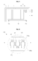
- FIG. 1 is a schematic view showing an organic light emitting display according to an embodiment
- FIG. 2 is a plan view showing "A" portion of FIG. 1 ;
- FIG. 3 is a vertical cross-sectional view taken along the line I-I of FIG. 2 ;
- FIG. 4 is a plan view showing a portion, which corresponds to FIG. 2 , of another example of an electrostatic discharge circuit
- FIG. 5 is a view showing other shapes of protruding electrodes of FIG. 4 ;
- FIG. 6 is a plan view showing a portion, which corresponds to FIG. 2 , of an organic light emitting display according to another embodiment
- FIG. 7 is a vertical cross-sectional view taken along the line II-II of FIG. 6 ;
- FIG. 8 is a schematic view showing an organic light emitting display according to another embodiment.
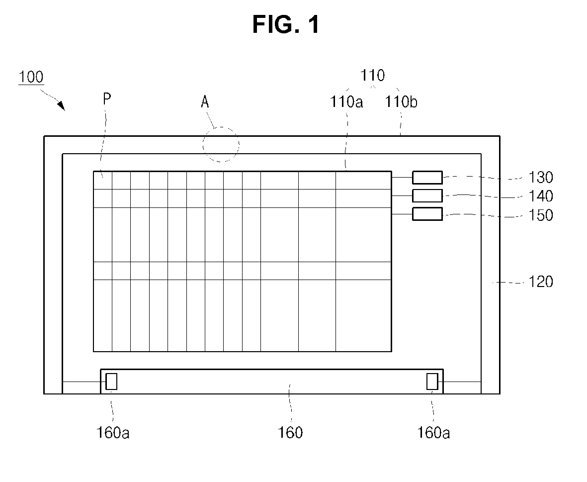
- FIG. 1 is a schematic view showing an organic light emitting display 100 according to an embodiment.
- the substrate 110 includes the pixel area 110a having approximately a rectangular shape and the non-pixel area 110b formed on the outer circumference of the pixel area 110a.
- the substrate 110 can be further electrically coupled with a data driver 130, a scan driver 140 and a light emission control driver 150.
- the pixel area 110a is an area that displays an image by driving a plurality of pixels arranged in the form of a matrix. Each pixel is formed near an area where a data line (not shown), a scan line (not shown) and a light emission control line (not shown) intersect with each other.
- each of the pixels P can include a driving element formed by a thin film transistor, at least one switching element, a capacitive element and an organic light emitting diode.
- the non-pixel area 110b is formed on the substrate 110 surrounding the pixel area 110a.
- the electrostatic discharge circuit 120, the data driver 130 adapted for supplying a data signal for each of the data lines, the scan driver 140 adapted for supplying a scan signal for each of the scan lines and the light emission control driver 150 adapted for supplying a light emission control signal for each of the light emission control lines are preferably be formed.
- the non-pixel area 110b can include a pad 160 for electrically coupling the pixel P, the data driver 130, the scan driver 140 and the light emission control driver 150 with an external module adapted to supply image data and/or video data.
- the electrostatic discharge circuit 120 is formed on the non-pixel area 110b of the substrate 110.
- the electrostatic discharge circuit 120 can be formed to extend along one or more edges of the (preferably rectangular) substrate 110.
- the electrostatic discharge circuit 120 is formed on each side of the substrate 110 except a portion where the pad 160 is located.
- the electrostatic discharge circuit 120 can be formed as a single piece to surround each side of the substrate 110.
- the electrostatic discharge circuit 120 protects an inner part, for example, a driving element, a switching element or an organic light emitting diode included in the pixel from being damaged due to electrostatic discharge (ESD) which can occur during a manufacturing process or a subsequent handling process of the organic light emitting display 100.
- ESD electrostatic discharge
- the data driver 130, the scan driver 140 and the light emission control driver 150 can be placed on the non-pixel area 110b of the substrate 110 as an integrated circuit (IC).
- the data driver 130, the scan driver 140 and the light emission control driver 150 can be formed on the same layer as the layer forming a thin film transistor (not shown) included in the pixel P of the pixel area 110a.
- the data driver 130, the scan driver 140 and the light emission control driver 150 can be formed not on the substrate 110 but on another separate substrate.
- the pad 160 is formed on the non-pixel area 110b of the substrate 110.
- the pad 160 is formed on one side of the substrate 110, and is configured to electrically couple an external circuit module (not shown) with the drivers 130, 140 and 150, or is formed to electrically couple an external circuit module with the pixel P.
- the electrostatic discharge circuit 120 can be electrically coupled with a ground pad 160a that is formed on at least one side of the pad 160.
- the electrostatic discharge circuit 120 that is used for the organic light emitting display 100 according to some embodiments of the present invention will be described in further detail.
- FIG. 2 is a plan view showing the "A" portion of FIG. 1
- FIG. 3 is a vertical sectional view of the electrostatic discharge circuit 120 taken along the line I-I of FIG. 2 .
- the electrostatic discharge circuit 120 which will be described hereinafter, can be applied to the electrostatic discharge circuit 120 that is formed not only on a portion ("A" of FIG. 1 ) but also on all other areas of the substrate 110.
- the buffer layer 121 serves at least for preventing moisture (H 2 O), hydrogen (H 2 ), oxygen (O 2 ), etc. from penetrating through the substrate 110 and infiltrating into the electrostatic discharge circuit 120.
- the buffer layer 121 can be formed of a silicon oxide layer (SiO 2 ) a silicon nitride layer (Si 3 N 4 ), an organic layer and their equivalents that can be easily formed during a semiconductor process, but not limited thereto.
- the buffer layer 121 can be formed in a multilayer structure, or can be omitted.
- the gate insulating layer 122 is formed on the top surface of the buffer layer 121.
- the gate insulating layer 122 is formed between the gate electrode 123, which will be described later, and the buffer layer 121 to obtain the electrical desired insulating.
- the gate insulating layer 122 can be formed of any of a silicon oxide layer, a silicon nitride layer, an organic layer or their equivalents that can be easily formed during a semiconductor process, but not limited thereto.
- the gate insulating layer 122 can be formed by any of a PECVD method, an LPCVD method, a sputtering method and other methods.
- the end e1 of the first protruding electrode 123a can be formed in an angular shape for allowing the static electricity charge to be concentrated for a relatively short time.
- the first protruding electrode 123a can be formed opposite to the second protruding electrode 125a which will be described later.
- the first protruding electrode 123a serves for concentrating the static electricity charge to the angular end e1 and forming a high electric field.
- the shape of the first protruding electrode 123a is not limited to that shown in FIG. 2 , however, the first protruding electrode can be formed in any shape that allows the static electricity charge to be concentrated.
- the insulating interlayer 124 is formed on top of the gate electrode 123.
- the insulating interlayer 124 can also be formed on the gate insulating layer 122 which is formed on the outer circumference of the gate electrode 123.
- the insulating interlayer 124 can be formed of the same insulating material as the gate insulating layer 122 and may include a silicon oxide layer, a silicon nitride layer, an organic layer and so on, but is not limited thereto.
- the insulating interlayer 124 can be formed of any of a polymer-based insulating material, a plastic-based insulating material, a glass-based insulating material and their equivalents, but is not limited thereto.
- the insulating interlayer 124 serves for inducing the break down of insulation by the static electricity applied through the gate electrode 123 or the source/drain electrode 125.
- the source/drain electrode 125 is formed on top of the insulating interlayer 124.
- the source/drain electrode 125 can be formed on the top of the insulating interlayer 124.
- the source/drain electrode 125 can be formed to be spaced apart from the gate electrode 123 in the horizontal direction.
- the source/drain electrode 125 can be electrically coupled with the ground pad 160a (see FIG. 1 ) formed on the pad 160 (see FIG. 1 ).
- the source/drain electrode 125 serves for inducing the break down of insulation of the insulating interlayer 124 formed between the source/drain electrode 125 and the gate electrode 123 and discharging the static electricity.
- the source/drain electrode 125 can ground the static electricity through the ground pad 160a (see FIG. 1 ).
- the source/drain electrode 125 can be formed of the same metal material as the gate electrode 123, but is not limited thereto.
- the source/drain electrode 125 can be deposited by any of, for example, a PECVD method, an LPCVD method, a sputtering method and their equivalent methods, and then can be patterned at the desired position in the desired number through processes of, for example, applying a photoresist, exposing, developing, etching and separating the photoresist.
- the source/drain electrode 125 can include the second protruding electrode 125a formed to extend horizontally in the source/drain electrode 125.
- the second protruding electrode 125a is formed to extend horizontally toward the gate electrode 123 in the source/drain electrode 125. As shown in FIG. 2 , the second protruding electrode 125a can be formed in the shape of a saw-tooth formed continuously in a portion of the source/drain electrode 125. Furthermore, the second protruding electrode 125a can be formed integrally with the source/drain electrode 125 and can be formed simultaneously with the source/drain electrode 125 in the process of forming the source/drain electrode 125. The second protruding electrode 125a can be formed such that its end e2 points toward the gate electrode 123 or the first protruding electrode 123a included in the gate electrode 123.
- the end e2 of the second protruding electrode 125a can be formed in an angular shape for allowing the static electricity charge to be concentrated.
- the second protruding electrode 125a serves for concentrating the static electricity charge to the angular end e2 and forming a high electric field.
- the distance (in the horizontal direction) between the source/drain electrode 125 and the gate electrode 123 can be varied depending on the voltage level of the static electricity to be controlled and the area of the electrostatic discharge circuit 120 to be formed in the non-pixel area 110b. 10b. If the voltage level of the static electricity to be controlled is relatively high (for example, above a few thousand volts), then the distance (in the horizontal direction) between the source/drain electrode 125 and the gate electrode 123 is formed as long as possible within the area able to forming the electrostatic discharge circuit 120. However, the distance (in the horizontal direction) between the source/drain electrode 125 and the gate electrode 123 is not limited.
- the electrostatic discharge circuit 120 can further include a protective layer formed on the source/drain electrode 125.
- the protective layer can include the first protective layer 126 and the second protective layer 127.
- the first protective layer 126 is formed to cover the source/drain electrode 125 and the insulating interlayer 124 and serves for protecting the source/drain electrode 125 and the gate electrode 123.
- the first protective layer 126 can be formed of any one selected from an ordinary organic layer and its equivalents, but is not limited thereto.
- the second protective layer 127 is formed to cover the first protective layer 126 and serves for aiding the surface of the electrostatic discharge circuit 120 to be substantially planar.
- the second protective layer 127 can be formed of at least one of benzo cyclo butene (BCB), acryl and their equivalents, but is not limited thereto.
- the electrostatic discharge circuit 120 can further include the third electrode layer 128 on the top surface of the second protective layer 127.
- the third electrode layer 128 is electrically coupled with the source/drain electrode 125 through an electrically conductive via hole v1.
- the third electrode layer 128 can be formed of the same metal material as the gate electrode 123 and the source/drain electrode 125, but is not limited thereto.
- the third electrode layer 128 aids the static electricity to be discharged to the source/drain electrode 125 through the electrically conductive via hole v1 when the static electricity is generated.
- the electrostatic discharge circuit 120 is formed on at least one side of the non-pixel area 110b which is on the outer circumference of the pixel area 110a of the organic light emitting display 100, and prevents the pixels P and the drivers 130, 140 and 150 from being damaged due to the electrostatic discharge.
- the electrostatic discharge current is conducted through the insulating interlayer 124 between the gate electrode 123 and the source/drain electrode 125.
- the static electricity from the gate electrode 123 or the source/drain electrode 125 is discharged by the break down of insulation of the insulating interlayer 124.
- a portion of the static electricity can be grounded by any one of the gate electrode 123 and the source/drain electrode 125.
- the static electricity generated in the outside of the electrostatic discharge circuit 120 can be transferred to the source/drain electrode 125 through the third electrode layer 128 and can be discharged thereby.
- the electrostatic discharge circuit 120 has an advantageous effect that allows the static electricity to be relatively easily dissipated with the first protruding electrode 123a and the second protruding electrode 125a which form a high electric field due to the concentration of the static electricity charge and thus facilitating the break down of the insulation.
- the ends e1 and e2 of the first and second protruding electrodes 123a and 125a are formed in an angular shape.
- the static electricity charge is concentrated at the ends e1 and e2 when the static electricity is generated, and thus relatively high electric field can be formed at the ends e1 and e2.
- the end e1 of the first protruding electrode 123a and the end e2 of the second protruding electrode 125a face each other, and the break down of insulation of the insulating interlayer 124 between the first protruding electrode 123a and the second protruding electrode 125a by the electrostatic discharge is facilitated. Accordingly, the electrostatic discharge can be dissipated more easily by the first protruding electrode 123a and the second protruding electrode 125a.
- FIG. 4 is a view showing a portion, which corresponds to FIG. 2 , of another electrostatic discharge circuit 120'
- FIG. 5 is a view showing other shapes of protruding electrodes 123a' and 125a' of FIG. 4 .
- the electrostatic discharge circuit 120' is similar to that of the electrostatic discharge circuit 120 of FIGS. 2 and 3 . An explanation of the protruding electrodes 123a' and 125a' will be made hereinafter.
- the first protruding electrode 123a' and the second protruding electrode 125a' can be formed on at least a portion of the gate electrode 123 and the source/drain electrode 125 in the form of a triangle, respectively.
- the first protruding electrode 123a' and the second protruding electrode 125a' can be formed such that one side thereof is formed on the gate electrode 123 and the source/drain electrode 125 and a vertex which is opposite to the one side points toward the opposite electrode respectively. That is, in the first protruding electrode 123a' and the second protruding electrode 125a' formed in the form of a triangle, the above-mentioned vertices can be ends e1' and e2'.
- the end e1' of the first protruding electrode 123a' and the end e2' of the second protruding electrode 125a' can be formed facing each other.
- the ends e1' and e2', which are formed on the protruding electrodes 123a' and 125a' respectively, are formed as the vertices, and thus perform similarly to the operation as the above-described embodiment.
- the static electricity charge transferred through the gate electrode 123 and the source/drain electrode 125 is concentrated to the ends e1' and e2', and relatively high electric field is formed between the ends e1' and e2', and thus the break down of insulation between the gate electrode 123 and the source/drain electrode 125 (the break down of insulation through the insulating interlayer 124) can be facilitated.
- each of the first protruding electrode 123a' and the second protruding electrode 125a' can be formed in the form of any of a rectangle a1', a pentagon a2' and a trapezoid a3'.
- the shapes of the first protruding electrode 123a' and the second protruding electrode 125a' are not limited thereto, and the shapes thereof can be varied.
- the first protruding electrode 123a' and the second protruding electrode 125a' have an advantageous aspect that they can be formed at the desired position of the gate electrode 123 and the source/drain electrode 125 in the desired number respectively. Accordingly, by forming the protruding electrodes 123a' and 125a' on a portion where the static electricity is intensively generated or a portion vulnerable to the static electricity, the break down of insulation by the static electricity can be more easily induced.
- an electrostatic discharge circuit 220 of the organic light emitting display includes a buffer layer 221 formed on the top of a substrate 210, a semiconductor layer 229 formed on the top of the buffer layer 221, a gate insulating layer 222 formed on the top of the semiconductor layer 229, a gate electrode 223 formed on the top of the gate insulating layer 222, an insulating interlayer 224 formed to cover the gate electrode 223, and a source/drain electrode 225 formed on the top of the insulating interlayer 224.
- the electrostatic discharge circuit 220 can further include a first protective layer 226 formed to cover the source/drain electrode 225, a second protective layer 227, and a third electrode layer 228 which is formed on the top surface of the second protective layer 227 and is electrically coupled with the source/drain electrode 225 through a via hole v2.
- the gate electrode 223 can include a first protruding electrode 223a formed to extend horizontally in the gate electrode 223.
- the source/drain electrode 225 can include a second protruding electrode 225a formed to extend horizontally in the source/drain electrode 225.
- the semiconductor layer 229 can be formed on the buffer layer 221 or the substrate 210.
- the semiconductor layer 229 serves for inducing the electrostatic discharge together with the gate electrode 23 and the source/drain electrode 225.
- the semiconductor layer 229 can be formed of any one selected from amorphous silicon, micro silicon (silicon having a grain size between amorphous silicon and polycrystalline silicon), an organic matter and their equivalents, but is not limited thereto.
- the semiconductor layer 229 can be electrically coupled with the source/drain electrode 225 through an electrically conductive contact c1 that is formed to penetrate the insulating interlayer 224.
- the semiconductor layer 229 includes source and drain areas (not shown) formed on both sides opposite to each other, a channel area (not shown) formed between the source and drain areas. After crystallizing amorphous silicon or micro silicon into polycrystalline silicon, the semiconductor layer 229 can be formed in the desired position and shape through patterning.
- the amorphous silicon can be crystallized by a laser crystallization method using an excimer laser, a metal induced crystallization (MIC) method using a metal promoting material, and a sold phase crystallization (SPC) method. Furthermore, there is a sequential lateral solidification (SLS) method which further uses a mask in the existing laser crystallization method.
- the laser crystallization method is the most widely used method. According to the laser crystallization method, it is possible to use the existing crystallization method of a polycrystalline liquid crystal display, the processing method is simple, and the technical development about the processing method has been completed.
- the metal induced crystallization method is one of methods that can crystallize at a low temperature without using the laser crystallization method.
- the metal induced crystallization method has an advantageous effect in that a metal promoting material such as Ni, Co, Pd, Ti, etc. is initially deposited or spin-coated on the surface of the amorphous silicon, and then the metal promoting material is directly penetrated into the surface of the amorphous silicon, thereby crystallizing the amorphous silicon at a low temperature while changing the phase thereof.
- Another metal induced crystallization method that uses a mask when applying a metal layer on the surface of the amorphous silicon is to prevent a contaminant such as a nickel silicide from depositing on a specific area of a thin film transistor.
- This crystallization method is referred to as a metal induced lateral crystallization (MILC) method.
- the mask used for the metal induced lateral crystallization method may be a shadow mask, and the shadow mask may be a linear mask or a dotted mask.
- Another metal induced crystallization method is a metal induced crystallization with capping layer (MICC) method which applies the capping layer on the surface of the amorphous silicon before depositing or spin-coating the metal promoting material layer thereon and controls the amount of a metal promoting material introduced into the amorphous silicon.
- MIBC metal induced crystallization with capping layer
- a silicon nitride layer can be used as the capping layer.
- the amount of the metal promoting material to be introduced into the amorphous silicon from the metal promoting material layer varies depending on the thickness of the silicon nitride layer.
- the metal promoting material introduced into the silicon nitride layer can be formed on the entire silicon nitride layer or can be selectively formed by using the shadow mask.
- the metal promoting material layer crystallizes the amorphous silicon into the polycrystalline silicon, it is possible to selectively remove the capping layer.
- a method for removing the capping layer a wet etching method or a dry etching method can be used.
- the micro silicon typically refers to silicon having a crystal grain size of 1nm to 100nm.
- the micro silicon is characterized in that its electron mobility is from 1 to 50 and its hole mobility is from 0.01 to 0.2.
- the micro silicon is characterized in that its crystal grain size is smaller than that of the polycrystalline silicon. Furthermore, a protrusion area between crystal grains of the micro silicon is formed small, and thus electron movement between the crystal grains does not hindered, thereby exhibiting uniform characteristics.
- a method for crystallizing the micro silicon there are a thermal crystallization method and a laser crystallization method.
- the thermal crystallization method includes a method that obtains a crystallization structure simultaneously with the deposition of the amorphous silicon, and a reheating method.
- the laser crystallization method is a crystallization method that crystallizes using a laser after depositing the amorphous silicon by a chemical vapor deposition method, and the laser employed is mainly a diode laser.
- the diode laser mainly uses a red wavelength of 800nm range, and the red wavelength serves for allowing the micro silicon to be uniformly crystallized.
- the polycrystalline silicon formed by the above-mentioned method is positioned at the desired position in the desired number through processes of applying a photoresist, exposing, developing, etching, separating the photoresist and so on.
- the electrostatic discharge circuit 220 is not operated when a usual driving voltage is applied.
- first protruding electrode 223a and the second protruding electrode 225a can be formed in a similar manner as the first protruding electrode 123a and the second protruding electrode 125a of the above-mentioned embodiments, and the operation of the first protruding electrode 223a and the second protruding electrode 225a is similar to the operation of the first protruding electrode 123a and the second protruding electrode 125a.
- the electrostatic discharge circuit 220 has an advantageous effect that since the static electricity can be discharged through the insulating interlayer 224 formed between the gate electrode 223 and the source/drain electrode 225 and the electrostatic discharge current can be conducted through the gate insulating layer 222 formed between the gate electrode 223 and the semiconductor layer 229 or through the gate insulating layer 222 and the insulating interlayer 224 between the source/drain electrode 225 and the semiconductor layer 229, it is possible to dissipate the electrostatic discharge by using other paths also.
- FIG. 8 is a schematic view showing an organic light emitting display according to yet another embodiment.
- the organic light emitting display 300 includes an electrostatic discharge circuit 320 that is separately formed on each side of a substrate 310 including a pixel area 310a and a non-pixel area 310b.
- the electrostatic discharge circuit 320 can be selectively formed only on an area where the electrostatic discharge is expected to occur, or another desired area.
- each electrostatic discharge circuit 320 can be electrically coupled with a ground pad (not shown) of a pad 360 formed on the substrate 310.
- the detailed structure of the electrostatic discharge circuit 320 according to this embodiment can be formed in a similar manner as the above-mentioned embodiments and the operation and the advantageous effect of the electrostatic discharge circuit 320 is also similar the above-mentioned embodiments.
- the organic light emitting diode included in the pixel P comprises, for example, an anode (ITO), an organic layer and a cathode (metal).
- the organic layer can be composed of an emitting layer (EML) which emits light by recombining electrons and holes and forming excitons, an electron transport layer (ETL) which transports electrons, and a hole transport layer (HTL) which transports holes.
- EML emitting layer
- ETL electron transport layer
- HTL hole transport layer
- the organic layer can be formed as a slim organic light emitting diode with two kinds of layers with reduced thickness. For example, it is possible to selectively form a hole injection transport layer (HITL) forming the hole injecting layer and the hole transport layer simultaneously and an electron injection transport layer (EITL) forming the electron injecting layer and the electron transport layer simultaneously.
- HITL hole injection transport layer
- EITL electron injection transport layer
- the slim organic light emitting diode is used to increase the light emission efficiency.
- a buffer layer can be formed between the anode (ITO) and the emitting layer as an optional layer. The buffer layer is divided into an electron buffer layer for buffering an electron and a hole buffer layer for buffering a hole.
- the electron buffer layer can be selectively formed between the cathode (metal) and the electron injecting layer (EIL) and can function as a substitute for the electron injecting layer (EIL).
- the stack structure of the organic layer can be the emission layer (EML)/electron transport layer (ETL)/electron buffer layer/cathode (metal).
- the hole buffer layer can be selectively formed between the anode (ITO) and the hole injecting layer (HIL) and can function as a substitute for the hole injecting layer (HIL).
- the stack structure of the organic layer can be the anode (ITO)/hole buffer layer/hole transport layer (HTL)/emission layer (EML).
- a passive matrix method As a method for driving the organic light emitting diode, either a passive matrix method or an active matrix method may be used.
- the passive matrix method has an advantageous effect of simple manufacturing process and less investment cost by forming the anode and the cathode to intersect at right angles and selecting and driving a line.
- the passive matrix method has a disadvantage of high current consumption when embodying a wide screen.
- the active matrix method has an advantageous effect of low current consumption, excellent image quality, long service life, and applicability to medium and large sized product by forming an active element such as a thin film transistor and a capacitive element on each pixel.
- the electrostatic discharge can be dissipated using the semiconductor layer in addition to the gate electrode and the source/drain electrode by forming the semiconductor layer in the electrostatic discharge circuit, and thus the electrostatic discharge can be dissipated using more various paths.
Landscapes
- Engineering & Computer Science (AREA)
- Microelectronics & Electronic Packaging (AREA)
- Electroluminescent Light Sources (AREA)
- Devices For Indicating Variable Information By Combining Individual Elements (AREA)
Abstract
Description
- This application claims the benefit of
Korean Patent Application No. 10-2007-0006306, filed on January 19, 2007 - The invention relates to an organic light emitting display, and more particularly, to an organic light emitting display that can prevent a pixel and a driver included in the organic light emitting display from being damaged due to electrostatic discharge.
- An organic light emitting display is a kind of flat panel display and uses an organic light emitting diode (OLED) which emits light by recombination of electrons supplied from a cathode with holes supplied from an anode. The organic light emitting display has advantageous aspects of being thin, having a wide viewing angle, and having a short response time.
- Methods for driving the organic light emitting display include a passive matrix method and an active matrix method. The passive matrix method is a method that selects and drives a line where an anode and a cathode intersect at right angles. On the other hand, the active matrix method is a method that realizes an image by supplying an organic light emitting diode (OLED) with a driving current corresponding to a data signal. The organic light emitting diode (OLED) uses a thin film transistor (TFT) formed on each pixel. The active matrix method has an advantageous aspect that it can exhibit more stable brightness and can consume less power than the passive matrix method, and thus it can be applied to large and high-resolution displays.
- A conventional organic light emitting display comprises a pixel area including a pixel matrix and a non-pixel area including a power supply and a driver for driving the plurality of pixels. The pixels are located in the pixel area and each pixel includes a thin film transistor and an organic light emitting diode for a driving operation or a switching operation. The pixel area and the non-pixel area are electrically coupled with each other through a plurality of lines.
- The conventional organic light emitting display is manufactured by forming a thin film transistor, forming an organic light emitting diode, encapsulating, and packaging. During such manufacturing steps, static electricity can be generated in the organic light emitting display by internal environmental factors or by external environmental factors. The static electricity can be generated during nearly all manufacturing processes for manufacturing the organic light emitting display including a deposition process, an etching process, etc. Furthermore, the static electricity can also be generated by an external environmental factor during displaying an image on the organic light emitting display.
- According to the conventional light emitting display, a problem is that an internal circuit is damaged due to electrostatic discharge (ESD) that occurs during the above-mentioned or other manufacturing steps or by an external environmental factor.
- Some aspects solve the aforementioned problems of the conventional organic light emitting display and provide an organic light emitting display that can prevent a pixel and a drive included in the organic light emitting display from being damaged due to electrostatic discharge.
- One aspect is an organic light emitting display including a (preferably planar) substrate including a pixel area and a non-pixel area (the pixel area being completely different from the non-pixel area, and preferably the pixel area being located adjacent to the non-pixel area), and an electrostatic discharge circuit formed in the non-pixel area (preferably being completely located within the non-pixel area and not being located within the pixel area), the electrostatic discharge circuit including a first electrode layer (first conductive layer) formed on the substrate, a first insulating layer formed on the first electrode layer, and a second electrode layer (second conductive layer) formed on the first insulating layer, where at least one of the first electrode layer and the second electrode layer includes a protruding electrode (protruding member or protruding portion) formed to extend horizontally toward the other of the first electrode layer and the second electrode layer.
The protruding members preferably comprise at least one spike or tooth having an angular shape for allowing the static electricity charge to be concentrated for a relatively short time.
The protruding members preferably comprise a plurality of spikes (or teeth) adapted to concentrate static electricity for a relatively short time (for a time below 1 s), the spikes more preferably a triangle shape (and still more preferably an equilateral or an isosceles triangle).
Preferably the protruding electrode substantially has the shape of any of a saw-tooth, a triangle, a rectangle, a pentagon and a trapezoid. Preferably the protruding electrode comprises a first protruding electrode included in the first electrode layer, and the first protruding electrode is formed to point horizontally toward the second electrode layer. Preferably the protruding electrode comprises an second protruding electrode included in the second electrode layer, and the second protruding electrode is formed to point horizontally toward the first electrode layer.
Preferably each of the first electrode layer and the second electrode layer comprises a protruding electrode formed to extend horizontally toward the other of the first electrode layer and the second electrode layer. Preferably the protruding electrodes extend toward one another.
Preferably the electrostatic discharge circuit further comprises a semiconductor layer formed between the substrate and the first electrode layer. Preferably the electrostatic discharge circuit further comprises a second insulating layer formed between the semiconductor layer and the first electrode layer. Preferably the electrostatic discharge circuit further comprises a buffer layer formed between the substrate and the semiconductor layer.
Preferably the electrostatic discharge circuit further comprises a protective layer formed on the second electrode layer. Preferably the electrostatic discharge circuit further comprises a third electrode layer formed on the protective layer and is electrically coupled with the second electrode layer through a via hole.
Preferably the non-pixel area further comprises: at least one driver configured to drive a pixel in the pixel area; and a pad configured to electrically couple the pixel and the driver with an external module. Preferably the pad is formed on at least one side of the inner circumference of the substrate. Preferably the electrostatic discharge circuit is formed on at least one side of the inner circumference of the substrate other than a side on which the pad is formed.
Preferably the electrostatic discharge circuit is separately formed on each side of the inner circumference of the substrate. Alternatively, the electrostatic discharge circuit is integrally formed to substantially surround the inner circumference of the substrate. Preferably any of the first electrode layer and the second electrode layer is electrically coupled with a ground pad. Preferably the first electrode layer and the second electrode layer comprises at least one of aluminum, aluminum-neodymium, chrome, molybdenum, molybdenum-tungsten and titanium. Preferably the first insulating layer comprises at least one of silicon oxide, silicon nitride and an organic matter.
Furthermore, the pad and drivers (such as data driver, scan driver and emission control driver) are preferably located completely within the non-pixel area.
The expression electrostatic discharge circuit does not necessarily mean that conductive lines are formed as a closed loop, however, the expression electrostatic discharge circuit means that at least two conductive layers are arranged such that a breakdown of an insulating layer therebetween can be induced (or controlled) and therefore static electricity can be discharged. - Another aspect is an organic light emitting display including a substrate including a pixel area and a non-pixel area, and an electrostatic discharge circuit in the non-pixel area, the electrostatic discharge circuit including a semiconductor layer formed on the substrate, a gate insulating layer formed on the semiconductor layer, a gate electrode formed on the gate insulating layer, an insulating interlayer formed to cover the gate electrode, and a source/drain electrode formed on the insulating interlayer, where the gate electrode includes a first protruding electrode formed to extend horizontally toward the source/drain electrode.
Preferably the source/drain electrode comprises a second protruding electrode formed to extend horizontally toward the gate electrode. Preferably the first protruding electrode and the second protruding electrode are formed in the shape of any of a saw-tooth, a triangle, a rectangle, a pentagon and a trapezoid. Preferably the electrostatic discharge circuit is formed such that the first protruding electrode and the second protruding electrode extend toward one another.
Preferably at least one of the gate electrode and the source/drain electrode is electrically coupled with a ground pad. Preferably the electrostatic discharge circuit further comprises a buffer layer formed between the substrate and the semiconductor layer. Preferably the electrostatic discharge circuit further comprises a protective layer formed on the source/drain electrode. Preferably the electrostatic discharge circuit further comprises an electrode layer formed on the protective layer and is electrically coupled with the source/drain electrode. - The above and other objects, features and advantages will be more apparent from the following detailed description taken in conjunction with the accompanying drawings, in which:
-
FIG. 1 is a schematic view showing an organic light emitting display according to an embodiment; -
FIG. 2 is a plan view showing "A" portion ofFIG. 1 ; -
FIG. 3 is a vertical cross-sectional view taken along the line I-I ofFIG. 2 ; -
FIG. 4 is a plan view showing a portion, which corresponds toFIG. 2 , of another example of an electrostatic discharge circuit; -
FIG. 5 is a view showing other shapes of protruding electrodes ofFIG. 4 ; -
FIG. 6 is a plan view showing a portion, which corresponds toFIG. 2 , of an organic light emitting display according to another embodiment; -
FIG. 7 is a vertical cross-sectional view taken along the line II-II ofFIG. 6 ; and -
FIG. 8 is a schematic view showing an organic light emitting display according to another embodiment. - Hereinafter, certain embodiments will be described with reference to the accompanying drawings. In the drawings, for the purpose of clear explanation, portions that are not related to such an explanation will be sometimes omitted.
- An organic light emitting display according to an embodiment will be explained.
-
FIG. 1 is a schematic view showing an organiclight emitting display 100 according to an embodiment. - Referring to
FIG. 1 , an organiclight emitting display 100 according to an embodiment includes: asubstrate 110 which includes apixel area 110a including pixels P arranged in the form of a matrix and anon-pixel area 110b formed on the outer circumference of thepixel area 110a; and anelectrostatic discharge circuit 120 formed on thenon-pixel area 110b. - The
substrate 110 includes thepixel area 110a having approximately a rectangular shape and thenon-pixel area 110b formed on the outer circumference of thepixel area 110a. Thesubstrate 110 can be further electrically coupled with adata driver 130, ascan driver 140 and a lightemission control driver 150. - The
pixel area 110a is an area that displays an image by driving a plurality of pixels arranged in the form of a matrix. Each pixel is formed near an area where a data line (not shown), a scan line (not shown) and a light emission control line (not shown) intersect with each other. Although not shown inFIG. 1 , each of the pixels P can include a driving element formed by a thin film transistor, at least one switching element, a capacitive element and an organic light emitting diode. - The
non-pixel area 110b is formed on thesubstrate 110 surrounding thepixel area 110a. In thenon-pixel area 110b, theelectrostatic discharge circuit 120, thedata driver 130 adapted for supplying a data signal for each of the data lines, thescan driver 140 adapted for supplying a scan signal for each of the scan lines and the lightemission control driver 150 adapted for supplying a light emission control signal for each of the light emission control lines are preferably be formed. Furthermore, thenon-pixel area 110b can include apad 160 for electrically coupling the pixel P, thedata driver 130, thescan driver 140 and the lightemission control driver 150 with an external module adapted to supply image data and/or video data. - The
electrostatic discharge circuit 120 is formed on thenon-pixel area 110b of thesubstrate 110. Theelectrostatic discharge circuit 120 can be formed to extend along one or more edges of the (preferably rectangular)substrate 110. In this embodiment, theelectrostatic discharge circuit 120 is formed on each side of thesubstrate 110 except a portion where thepad 160 is located. Theelectrostatic discharge circuit 120 can be formed as a single piece to surround each side of thesubstrate 110. Theelectrostatic discharge circuit 120 protects an inner part, for example, a driving element, a switching element or an organic light emitting diode included in the pixel from being damaged due to electrostatic discharge (ESD) which can occur during a manufacturing process or a subsequent handling process of the organiclight emitting display 100. Theelectrostatic discharge circuit 120 can also protect circuits formed on thenon-pixel area 110b such as thedata driver 130, thescan driver 140, the lightemission control driver 150 and thepad 160 and so on which will be described later. Although theelectrostatic discharge circuit 120 has been described as being formed on at least one edge portion of thesubstrate 110, the invention is not limited thereto. Of course, theelectrostatic discharge circuit 120 can be formed on another area of thesubstrate 110 but preferably only and completely within thenon-pixel area 110b. A detailed structure of theelectrostatic discharge circuit 120 will be described later. - The
data driver 130, thescan driver 140 and the lightemission control driver 150 can be placed on thenon-pixel area 110b of thesubstrate 110 as an integrated circuit (IC). Thedata driver 130, thescan driver 140 and the lightemission control driver 150 can be formed on the same layer as the layer forming a thin film transistor (not shown) included in the pixel P of thepixel area 110a. On the other hand, thedata driver 130, thescan driver 140 and the lightemission control driver 150 can be formed not on thesubstrate 110 but on another separate substrate. Therespective drivers substrate 110 by any of, for example, a tape carrier package (TCP), a flexible printed circuit (FPC), a tape automated bonding (TAB), a chip on glass (COG) and their equivalents, but is not limited thereto. - The
pad 160 is formed on thenon-pixel area 110b of thesubstrate 110. Thepad 160 is formed on one side of thesubstrate 110, and is configured to electrically couple an external circuit module (not shown) with thedrivers electrostatic discharge circuit 120 can be electrically coupled with aground pad 160a that is formed on at least one side of thepad 160. - The
electrostatic discharge circuit 120 that is used for the organiclight emitting display 100 according to some embodiments of the present invention will be described in further detail. -
FIG. 2 is a plan view showing the "A" portion ofFIG. 1 , andFIG. 3 is a vertical sectional view of theelectrostatic discharge circuit 120 taken along the line I-I ofFIG. 2 . Theelectrostatic discharge circuit 120, which will be described hereinafter, can be applied to theelectrostatic discharge circuit 120 that is formed not only on a portion ("A" ofFIG. 1 ) but also on all other areas of thesubstrate 110. - Referring to
FIGS. 2 and3 , theelectrostatic discharge circuit 120 of the organiclight emitting display 100 according to a preferred embodiment of the invention includes abuffer layer 121 formed on the top of thesubstrate 110, agate insulating layer 122 formed on the top of thebuffer layer 121, a gate electrode 123 (optionally referred to as a "first electrode layer") formed on the top of thegate insulating layer 122, an insulating interlayer 124 (optionally referred to as a "first insulating layer") formed to cover thegate electrode 123, and a source/drain electrode 125 (optionally referred to as a "second electrode layer") formed on the top of the insulatinginterlayer 124. Furthermore, theelectrostatic discharge circuit 120 can further include a firstprotective layer 126 formed to cover the source/drain electrode 125, a secondprotective layer 127, and athird electrode layer 128 which is formed on the top surface of the secondprotective layer 127 and is electrically coupled with the source/drain electrode 125. In some embodiments, thegate electrode 123 can include a firstprotruding electrode 123a formed to extend horizontally. Furthermore, the source/drain electrode 125 can include a secondprotruding electrode 125a formed to extend horizontally. - The
substrate 110 is formed in the form of a plate with top and bottom surfaces, and the thickness between the top and bottom surfaces is from about 0.05mm to about 1mm. If the thickness of thesubstrate 110 is below about 0.05mm, a disadvantage is caused that the substrate is liable to damage during cleaning, etching and heat treatment processes and has a low resistance to an external force. Moreover, if the thickness of thesubstrate 110 is above about 1mm, it is difficult to apply the substrate to various display devices that are thin. Thesubstrate 110 can be formed of at least one of an ordinary glass, a plastic, a stainless steel and their equivalents, but not limited thereto. Thesubstrate 110 may be formed by pre-compacting thesubstrate 110 to prevent it from being readily deformed due to a heat or a pressure in the step of cleaning the substrate to prevent it from containing foreign substances and in the step of manufacturing other components. Thesubstrate 110 can be divided into thepixel area 110a including the thin film transistor and the organic light emitting diode and thenon-pixel area 110b on which various drivers are formed. - The
buffer layer 121 serves at least for preventing moisture (H2O), hydrogen (H2), oxygen (O2), etc. from penetrating through thesubstrate 110 and infiltrating into theelectrostatic discharge circuit 120. For this purpose, thebuffer layer 121 can be formed of a silicon oxide layer (SiO2) a silicon nitride layer (Si3N4), an organic layer and their equivalents that can be easily formed during a semiconductor process, but not limited thereto. Of course, thebuffer layer 121 can be formed in a multilayer structure, or can be omitted. - The
gate insulating layer 122 is formed on the top surface of thebuffer layer 121. Thegate insulating layer 122 is formed between thegate electrode 123, which will be described later, and thebuffer layer 121 to obtain the electrical desired insulating. Thegate insulating layer 122 can be formed of any of a silicon oxide layer, a silicon nitride layer, an organic layer or their equivalents that can be easily formed during a semiconductor process, but not limited thereto. Thegate insulating layer 122 can be formed by any of a PECVD method, an LPCVD method, a sputtering method and other methods. - The
gate electrode 123 is formed on the top of thegate insulating layer 122. Thegate electrode 123 can be electrically coupled with theground pad 160a (seeFIG. 1 ) included in the pad 160 (seeFIG 1 ). Thegate electrode 123 can be, for example, formed of any of aluminum (Al), aluminum-neodymium (AlNd), chrome (Cr), molybdenum (Mo), molybdenum-tungsten (MoW) and titanium (Ti) or can be formed of a metal material made by their combinations, but is not limited thereto. After being deposited on thegate insulating layer 122, thegate electrode 123 can be positioned at the desired position in the desired number through processes of applying a photoresist, exposing, developing, etching, separating the photoresist and so on. Thegate electrode 123 serves for inducing the break down of the insulatinginterlayer 124, which will be described later, and discharging the static electricity. Furthermore, thegate electrode 123 can ground the static electricity by theground pad 160a included in the pad 160 (seeFIG. 1 ). Thegate electrode 123 can include the first protrudingelectrode 123a for inducing relatively easily the electrostatic discharge. - The first
protruding electrode 123a is formed to extend horizontally toward the source/drain electrode 125, which will be described later, in thegate electrode 123. As shown inFIG. 2 , the first protrudingelectrode 123a can be formed in the shape of a saw-tooth formed in a portion of thegate electrode 123. Furthermore, the first protrudingelectrode 123a can be formed integrally with thegate electrode 123 and can be formed simultaneously with thegate electrode 123 in the process of forming thegate electrode 123. The firstprotruding electrode 123a can be formed such that its end e1 points toward the source/drain electrode 125 or the secondprotruding electrode 125a included in the source/drain electrode 125. The end e1 of the first protrudingelectrode 123a can be formed in an angular shape for allowing the static electricity charge to be concentrated for a relatively short time. The firstprotruding electrode 123a can be formed opposite to the secondprotruding electrode 125a which will be described later. In case that the electrostatic discharge occurs in thegate electrode 123, the first protrudingelectrode 123a serves for concentrating the static electricity charge to the angular end e1 and forming a high electric field. The shape of the first protrudingelectrode 123a is not limited to that shown inFIG. 2 , however, the first protruding electrode can be formed in any shape that allows the static electricity charge to be concentrated. - The insulating
interlayer 124 is formed on top of thegate electrode 123. Of course, the insulatinginterlayer 124 can also be formed on thegate insulating layer 122 which is formed on the outer circumference of thegate electrode 123. The insulatinginterlayer 124 can be formed of the same insulating material as thegate insulating layer 122 and may include a silicon oxide layer, a silicon nitride layer, an organic layer and so on, but is not limited thereto. The insulatinginterlayer 124 can be formed of any of a polymer-based insulating material, a plastic-based insulating material, a glass-based insulating material and their equivalents, but is not limited thereto. The insulatinginterlayer 124 serves for inducing the break down of insulation by the static electricity applied through thegate electrode 123 or the source/drain electrode 125. - The source/
drain electrode 125 is formed on top of the insulatinginterlayer 124. The source/drain electrode 125 can be formed on the top of the insulatinginterlayer 124. The source/drain electrode 125 can be formed to be spaced apart from thegate electrode 123 in the horizontal direction. The source/drain electrode 125 can be electrically coupled with theground pad 160a (seeFIG. 1 ) formed on the pad 160 (seeFIG. 1 ). The source/drain electrode 125 serves for inducing the break down of insulation of the insulatinginterlayer 124 formed between the source/drain electrode 125 and thegate electrode 123 and discharging the static electricity. The source/drain electrode 125 can ground the static electricity through theground pad 160a (seeFIG. 1 ). The source/drain electrode 125 can be formed of the same metal material as thegate electrode 123, but is not limited thereto. The source/drain electrode 125 can be deposited by any of, for example, a PECVD method, an LPCVD method, a sputtering method and their equivalent methods, and then can be patterned at the desired position in the desired number through processes of, for example, applying a photoresist, exposing, developing, etching and separating the photoresist. On the other hand, the source/drain electrode 125 can include the secondprotruding electrode 125a formed to extend horizontally in the source/drain electrode 125. - The second
protruding electrode 125a is formed to extend horizontally toward thegate electrode 123 in the source/drain electrode 125. As shown inFIG. 2 , the secondprotruding electrode 125a can be formed in the shape of a saw-tooth formed continuously in a portion of the source/drain electrode 125. Furthermore, the secondprotruding electrode 125a can be formed integrally with the source/drain electrode 125 and can be formed simultaneously with the source/drain electrode 125 in the process of forming the source/drain electrode 125. The secondprotruding electrode 125a can be formed such that its end e2 points toward thegate electrode 123 or the first protrudingelectrode 123a included in thegate electrode 123. Similarly to the end e1 of the first protrudingelectrode 123a, the end e2 of the secondprotruding electrode 125a can be formed in an angular shape for allowing the static electricity charge to be concentrated. In case that the electrostatic discharge occurs in the source/drain electrode 125, the secondprotruding electrode 125a serves for concentrating the static electricity charge to the angular end e2 and forming a high electric field. - Meanwhile, the distance (in the horizontal direction) between the source/
drain electrode 125 and thegate electrode 123 can be varied depending on the voltage level of the static electricity to be controlled and the area of theelectrostatic discharge circuit 120 to be formed in thenon-pixel area 110b. 10b. If the voltage level of the static electricity to be controlled is relatively high (for example, above a few thousand volts), then the distance (in the horizontal direction) between the source/drain electrode 125 and thegate electrode 123 is formed as long as possible within the area able to forming theelectrostatic discharge circuit 120. However, the distance (in the horizontal direction) between the source/drain electrode 125 and thegate electrode 123 is not limited. - The
electrostatic discharge circuit 120 can further include a protective layer formed on the source/drain electrode 125. The protective layer can include the firstprotective layer 126 and the secondprotective layer 127. The firstprotective layer 126 is formed to cover the source/drain electrode 125 and the insulatinginterlayer 124 and serves for protecting the source/drain electrode 125 and thegate electrode 123. The firstprotective layer 126 can be formed of any one selected from an ordinary organic layer and its equivalents, but is not limited thereto. Furthermore, the secondprotective layer 127 is formed to cover the firstprotective layer 126 and serves for aiding the surface of theelectrostatic discharge circuit 120 to be substantially planar. The secondprotective layer 127 can be formed of at least one of benzo cyclo butene (BCB), acryl and their equivalents, but is not limited thereto. - Furthermore, the
electrostatic discharge circuit 120 can further include thethird electrode layer 128 on the top surface of the secondprotective layer 127. Thethird electrode layer 128 is electrically coupled with the source/drain electrode 125 through an electrically conductive via hole v1. Thethird electrode layer 128 can be formed of the same metal material as thegate electrode 123 and the source/drain electrode 125, but is not limited thereto. Thethird electrode layer 128 aids the static electricity to be discharged to the source/drain electrode 125 through the electrically conductive via hole v1 when the static electricity is generated. - According to the above-mentioned embodiment, the
electrostatic discharge circuit 120 is formed on at least one side of thenon-pixel area 110b which is on the outer circumference of thepixel area 110a of the organiclight emitting display 100, and prevents the pixels P and thedrivers - More specifically, the electrostatic discharge current is conducted through the insulating
interlayer 124 between thegate electrode 123 and the source/drain electrode 125. The static electricity from thegate electrode 123 or the source/drain electrode 125 is discharged by the break down of insulation of the insulatinginterlayer 124. A portion of the static electricity can be grounded by any one of thegate electrode 123 and the source/drain electrode 125. Furthermore, the static electricity generated in the outside of theelectrostatic discharge circuit 120 can be transferred to the source/drain electrode 125 through thethird electrode layer 128 and can be discharged thereby. - The
electrostatic discharge circuit 120 has an advantageous effect that allows the static electricity to be relatively easily dissipated with the first protrudingelectrode 123a and the secondprotruding electrode 125a which form a high electric field due to the concentration of the static electricity charge and thus facilitating the break down of the insulation. - More specifically, the ends e1 and e2 of the first and second
protruding electrodes electrode 123a and the end e2 of the secondprotruding electrode 125a face each other, and the break down of insulation of the insulatinginterlayer 124 between the first protrudingelectrode 123a and the secondprotruding electrode 125a by the electrostatic discharge is facilitated. Accordingly, the electrostatic discharge can be dissipated more easily by the first protrudingelectrode 123a and the secondprotruding electrode 125a. - Next, another example of the protruding
electrodes electrostatic discharge circuit 120 will be described. -
FIG. 4 is a view showing a portion, which corresponds toFIG. 2 , of another electrostatic discharge circuit 120', andFIG. 5 is a view showing other shapes of protrudingelectrodes 123a' and 125a' ofFIG. 4 . - The electrostatic discharge circuit 120' is similar to that of the
electrostatic discharge circuit 120 ofFIGS. 2 and3 . An explanation of the protrudingelectrodes 123a' and 125a' will be made hereinafter. - The electrostatic discharge circuit 120' includes a first
protruding electrode 123a' formed to extend horizontally in thegate electrode 123 and a secondprotruding electrode 125a' formed to extend horizontally in the source/drain electrode 125. - The first
protruding electrode 123a' and the secondprotruding electrode 125a' can be formed on at least a portion of thegate electrode 123 and the source/drain electrode 125 in the form of a triangle, respectively. The firstprotruding electrode 123a' and the secondprotruding electrode 125a' can be formed such that one side thereof is formed on thegate electrode 123 and the source/drain electrode 125 and a vertex which is opposite to the one side points toward the opposite electrode respectively. That is, in the first protrudingelectrode 123a' and the secondprotruding electrode 125a' formed in the form of a triangle, the above-mentioned vertices can be ends e1' and e2'. The end e1' of the first protrudingelectrode 123a' and the end e2' of the secondprotruding electrode 125a' can be formed facing each other. As described above, the ends e1' and e2', which are formed on the protrudingelectrodes 123a' and 125a' respectively, are formed as the vertices, and thus perform similarly to the operation as the above-described embodiment. The static electricity charge transferred through thegate electrode 123 and the source/drain electrode 125 is concentrated to the ends e1' and e2', and relatively high electric field is formed between the ends e1' and e2', and thus the break down of insulation between thegate electrode 123 and the source/drain electrode 125 (the break down of insulation through the insulating interlayer 124) can be facilitated. - As shown in
FIG. 5 , each of the first protrudingelectrode 123a' and the secondprotruding electrode 125a' can be formed in the form of any of a rectangle a1', a pentagon a2' and a trapezoid a3'. However, the shapes of the first protrudingelectrode 123a' and the secondprotruding electrode 125a' are not limited thereto, and the shapes thereof can be varied. - The first
protruding electrode 123a' and the secondprotruding electrode 125a' have an advantageous aspect that they can be formed at the desired position of thegate electrode 123 and the source/drain electrode 125 in the desired number respectively. Accordingly, by forming the protrudingelectrodes 123a' and 125a' on a portion where the static electricity is intensively generated or a portion vulnerable to the static electricity, the break down of insulation by the static electricity can be more easily induced. - Next, an organic light emitting display according to another embodiment will be described hereinafter.
-
FIG. 6 is a plan view showing a portion, which corresponds toFIG. 2 , of an organic light emitting display according to another embodiment, andFIG. 7 is a vertical cross-sectional view taken along the line II-II ofFIG. 6 . Since the organic light emitting display of this embodiment is similar to that of the embodiment shown inFIGS. 1 to 4 , an explanation emphasizing the different features will be made hereinafter. - Referring to
FIGS. 6 and7 , anelectrostatic discharge circuit 220 of the organic light emitting display according to this embodiment includes abuffer layer 221 formed on the top of asubstrate 210, asemiconductor layer 229 formed on the top of thebuffer layer 221, agate insulating layer 222 formed on the top of thesemiconductor layer 229, agate electrode 223 formed on the top of thegate insulating layer 222, an insulatinginterlayer 224 formed to cover thegate electrode 223, and a source/drain electrode 225 formed on the top of the insulatinginterlayer 224. Furthermore, theelectrostatic discharge circuit 220 can further include a firstprotective layer 226 formed to cover the source/drain electrode 225, a secondprotective layer 227, and athird electrode layer 228 which is formed on the top surface of the secondprotective layer 227 and is electrically coupled with the source/drain electrode 225 through a via hole v2. Thegate electrode 223 can include a firstprotruding electrode 223a formed to extend horizontally in thegate electrode 223. Furthermore, the source/drain electrode 225 can include a secondprotruding electrode 225a formed to extend horizontally in the source/drain electrode 225. Some embodiments can be formed with the same structure and material as the above-mentioned embodiments except that thesemiconductor layer 229 is formed on the top of thebuffer layer 221. - The
semiconductor layer 229 can be formed on thebuffer layer 221 or thesubstrate 210. Thesemiconductor layer 229 serves for inducing the electrostatic discharge together with the gate electrode 23 and the source/drain electrode 225. Thesemiconductor layer 229 can be formed of any one selected from amorphous silicon, micro silicon (silicon having a grain size between amorphous silicon and polycrystalline silicon), an organic matter and their equivalents, but is not limited thereto. Thesemiconductor layer 229 can be electrically coupled with the source/drain electrode 225 through an electrically conductive contact c1 that is formed to penetrate the insulatinginterlayer 224. Thesemiconductor layer 229 includes source and drain areas (not shown) formed on both sides opposite to each other, a channel area (not shown) formed between the source and drain areas. After crystallizing amorphous silicon or micro silicon into polycrystalline silicon, thesemiconductor layer 229 can be formed in the desired position and shape through patterning. - The amorphous silicon can be crystallized by a laser crystallization method using an excimer laser, a metal induced crystallization (MIC) method using a metal promoting material, and a sold phase crystallization (SPC) method. Furthermore, there is a sequential lateral solidification (SLS) method which further uses a mask in the existing laser crystallization method. The laser crystallization method is the most widely used method. According to the laser crystallization method, it is possible to use the existing crystallization method of a polycrystalline liquid crystal display, the processing method is simple, and the technical development about the processing method has been completed.
- The metal induced crystallization method is one of methods that can crystallize at a low temperature without using the laser crystallization method. The metal induced crystallization method has an advantageous effect in that a metal promoting material such as Ni, Co, Pd, Ti, etc. is initially deposited or spin-coated on the surface of the amorphous silicon, and then the metal promoting material is directly penetrated into the surface of the amorphous silicon, thereby crystallizing the amorphous silicon at a low temperature while changing the phase thereof.
- Another metal induced crystallization method that uses a mask when applying a metal layer on the surface of the amorphous silicon is to prevent a contaminant such as a nickel silicide from depositing on a specific area of a thin film transistor. This crystallization method is referred to as a metal induced lateral crystallization (MILC) method. The mask used for the metal induced lateral crystallization method may be a shadow mask, and the shadow mask may be a linear mask or a dotted mask.
- Another metal induced crystallization method is a metal induced crystallization with capping layer (MICC) method which applies the capping layer on the surface of the amorphous silicon before depositing or spin-coating the metal promoting material layer thereon and controls the amount of a metal promoting material introduced into the amorphous silicon. As the capping layer, a silicon nitride layer can be used. The amount of the metal promoting material to be introduced into the amorphous silicon from the metal promoting material layer varies depending on the thickness of the silicon nitride layer. At this time, the metal promoting material introduced into the silicon nitride layer can be formed on the entire silicon nitride layer or can be selectively formed by using the shadow mask. After the metal promoting material layer crystallizes the amorphous silicon into the polycrystalline silicon, it is possible to selectively remove the capping layer. As a method for removing the capping layer, a wet etching method or a dry etching method can be used.
- The micro silicon typically refers to silicon having a crystal grain size of 1nm to 100nm. The micro silicon is characterized in that its electron mobility is from 1 to 50 and its hole mobility is from 0.01 to 0.2. The micro silicon is characterized in that its crystal grain size is smaller than that of the polycrystalline silicon. Furthermore, a protrusion area between crystal grains of the micro silicon is formed small, and thus electron movement between the crystal grains does not hindered, thereby exhibiting uniform characteristics. As a method for crystallizing the micro silicon, there are a thermal crystallization method and a laser crystallization method. The thermal crystallization method includes a method that obtains a crystallization structure simultaneously with the deposition of the amorphous silicon, and a reheating method. The laser crystallization method is a crystallization method that crystallizes using a laser after depositing the amorphous silicon by a chemical vapor deposition method, and the laser employed is mainly a diode laser. The diode laser mainly uses a red wavelength of 800nm range, and the red wavelength serves for allowing the micro silicon to be uniformly crystallized.
- The polycrystalline silicon formed by the above-mentioned method is positioned at the desired position in the desired number through processes of applying a photoresist, exposing, developing, etching, separating the photoresist and so on.
- In the source/
drain electrode 225, an electrode contacted with the source area and the drain area is integrally formed. Hence, theelectrostatic discharge circuit 220 is not operated when a usual driving voltage is applied. - Meanwhile, the first protruding
electrode 223a and the secondprotruding electrode 225a according to another embodiment can be formed in a similar manner as the first protrudingelectrode 123a and the secondprotruding electrode 125a of the above-mentioned embodiments, and the operation of the first protrudingelectrode 223a and the secondprotruding electrode 225a is similar to the operation of the first protrudingelectrode 123a and the secondprotruding electrode 125a. - According to the above-mentioned embodiments, the
electrostatic discharge circuit 220 has an advantageous effect that since the static electricity can be discharged through the insulatinginterlayer 224 formed between thegate electrode 223 and the source/drain electrode 225 and the electrostatic discharge current can be conducted through thegate insulating layer 222 formed between thegate electrode 223 and thesemiconductor layer 229 or through thegate insulating layer 222 and the insulatinginterlayer 224 between the source/drain electrode 225 and thesemiconductor layer 229, it is possible to dissipate the electrostatic discharge by using other paths also. - Furthermore, by forming the first protruding
electrode 223a and the secondprotruding electrode 225a, at which the static electricity is concentrated, on thegate electrode 223 and the source/drain electrode 225, it is possible to dissipated more easily the electrostatic discharge current. The operation of the firstprotruding electrode 223 and the secondprotruding electrode 225a is similar to the operation of the above-mentioned embodiments. -
FIG. 8 is a schematic view showing an organic light emitting display according to yet another embodiment. - Referring to
FIG. 8 , the organiclight emitting display 300 according to yet another embodiment includes anelectrostatic discharge circuit 320 that is separately formed on each side of asubstrate 310 including apixel area 310a and anon-pixel area 310b. Hence, it is an advantageous effect that theelectrostatic discharge circuit 320 can be selectively formed only on an area where the electrostatic discharge is expected to occur, or another desired area. According to yet another embodiment eachelectrostatic discharge circuit 320 can be electrically coupled with a ground pad (not shown) of apad 360 formed on thesubstrate 310. The detailed structure of theelectrostatic discharge circuit 320 according to this embodiment can be formed in a similar manner as the above-mentioned embodiments and the operation and the advantageous effect of theelectrostatic discharge circuit 320 is also similar the above-mentioned embodiments. - The organic light emitting diode included in the pixel P comprises, for example, an anode (ITO), an organic layer and a cathode (metal). The organic layer can be composed of an emitting layer (EML) which emits light by recombining electrons and holes and forming excitons, an electron transport layer (ETL) which transports electrons, and a hole transport layer (HTL) which transports holes. Furthermore, an electron injecting layer (EIL) which injects electrons can be formed on one side of the electron transport layer, and a hole injecting layer (HIL) which injects holes can be formed on one side of the hole transport layer. Moreover, in case of a phosphorescent organic light emitting diode, a hole blocking layer (HBL) can be selectively formed between the emitting layer (EML) and the electron transport layer (ETL), and an electron blocking layer (EBL) can be selectively formed between the emitting layer (EML) and the hole transport layer (HTL).
- Furthermore, the organic layer can be formed as a slim organic light emitting diode with two kinds of layers with reduced thickness. For example, it is possible to selectively form a hole injection transport layer (HITL) forming the hole injecting layer and the hole transport layer simultaneously and an electron injection transport layer (EITL) forming the electron injecting layer and the electron transport layer simultaneously. The slim organic light emitting diode is used to increase the light emission efficiency. Furthermore, a buffer layer can be formed between the anode (ITO) and the emitting layer as an optional layer. The buffer layer is divided into an electron buffer layer for buffering an electron and a hole buffer layer for buffering a hole.
- The electron buffer layer can be selectively formed between the cathode (metal) and the electron injecting layer (EIL) and can function as a substitute for the electron injecting layer (EIL). The stack structure of the organic layer can be the emission layer (EML)/electron transport layer (ETL)/electron buffer layer/cathode (metal). Furthermore, the hole buffer layer can be selectively formed between the anode (ITO) and the hole injecting layer (HIL) and can function as a substitute for the hole injecting layer (HIL). At this time, the stack structure of the organic layer can be the anode (ITO)/hole buffer layer/hole transport layer (HTL)/emission layer (EML).
- Possible stack structures are as follows:
- a) Normal Stack Structure
- 1) the anode/hole injecting layer/hole transport layer/emitting layer/electron transport layer/electron injecting layer/cathode
- 2) the anode/hole buffer layer/hole injecting layer/hole transport layer/emitting layer/electron transport layer/electron injecting layer/cathode
- 3) the anode/hole injecting layer/hole transport layer/emitting layer/electron transport layer/electron injecting layer/electron buffer layer/cathode
- 4) the anode/hole buffer layer/hole injecting layer/hole transport layer/emitting layer/electron transport layer/electron injecting layer/electron buffer layer/cathode
- 5) the anode/hole injecting layer/hole buffer layer/hole transport layer/emitting layer/electron transport layer/electron injecting layer/cathode
- 6) the anode/hole injecting layer/hole transport layer/emitting layer/electron transport layer/electron buffer layer/electron injecting layer/cathode
- b) Normal Slim Structure
- 1) the anode/hole injection transport layer/emitting layer/electron transport layer/electron injecting layer/cathode
- 2) the anode/hole buffer layer/hole injection transport layer/emitting layer/electron transport layer/electron injecting layer/cathode
- 3) the anode/hole injecting layer/hole transport layer/emitting layer/electron injection transport layer/electron buffer layer/cathode
- 4) the anode/hole buffer layer/hole transport layer/emitting layer/electron injection transport layer/electron buffer layer/cathode
- 5) the anode/hole injection transport layer/hole buffer layer/emitting layer/electron transport layer/electron injecting layer/cathode
- 6) the anode/hole injecting layer/hole transport layer/emitting layer/electron buffer layer/electron injection transport layer/cathode
- c) Inverted Stack Structure
- 1) the cathode/electron injecting layer/electron transport layer/emitting layer/hole transport layer/hole injecting layer/anode
- 2) the cathode/electron injecting layer/electron transport layer/emitting layer/hole transport layer/hole injecting layer/hole buffer layer/anode
- 3) the cathode/electron buffer layer/electron injecting layer/electron transport layer/emitting layer/hole transport layer/hole injecting layer/anode
- 4) the cathode/electron buffer layer/electron injecting layer/electron transport layer/emitting layer/hole transport layer/hole buffer layer/anode
- 5) the cathode/electron injecting layer/electron transport layer/emitting layer/hole transport layer/hole buffer layer/hole injecting layer/anode
- 6) the cathode/electron injecting layer/electron buffer layer/electron transport layer/emitting layer/hole transport layer/hole injecting layer/anode
- d) Inverted Slim Structure
- 1) the cathode/electron injecting layer/electron transport layer/emitting layer/hole injection transport layer/anode
- 2) the cathode/electron injecting layer/electron transport layer/emitting layer/hole injection transport layer/hole buffer layer/anode
- 3) the cathode/electron buffer layer/electron injection transport layer/emitting layer/hole transport layer/hole injecting layer/anode
- 4) the cathode/electron buffer layer/electron injection transport layer/emitting layer/hole transport layer/hole buffer layer/anode
- 5) the cathode/electron injecting layer/electron transport layer/emitting layer/hole buffer layer/hole injection transport layer/anode
- 6) the cathode/electron injection transport layer/electron buffer layer/emitting layer/hole transport layer/hole injecting layer/anode
- As a method for driving the organic light emitting diode, either a passive matrix method or an active matrix method may be used. The passive matrix method has an advantageous effect of simple manufacturing process and less investment cost by forming the anode and the cathode to intersect at right angles and selecting and driving a line. However, the passive matrix method has a disadvantage of high current consumption when embodying a wide screen. The active matrix method has an advantageous effect of low current consumption, excellent image quality, long service life, and applicability to medium and large sized product by forming an active element such as a thin film transistor and a capacitive element on each pixel.
- According to the above-mentioned embodiments, the organic light emitting display is provided on at least one side of the substrate with the electrostatic discharge circuit, and thus can prevent the pixels or the drives from being damaged due to the electrostatic discharge generated by environmental causes, whether internal or external to the display. At this time, the electrostatic discharge circuit includes the protruding electrode that concentrates the static electricity charge and forms a high electric field, and thus can dissipate more easily the electrostatic discharge current.
- As described above, the organic light emitting display has an advantageous effect that can prevent the pixels or the drivers from being damaged due to the electrostatic discharge by forming the electrostatic discharge circuit on at least one side of the inner circumference of the substrate.
- Furthermore, such an advantageous effect is attained that the break down of insulation between the protruding electrodes can be more facilitated by forming the protruding electrodes to extend horizontally on the gate electrode and the source/drain electrode of the electrostatic discharge circuit respectively, and thus the electrostatic discharge can be more easily dissipated.
- Moreover, such an advantageous effect is attained that the electrostatic discharge can be dissipated using the semiconductor layer in addition to the gate electrode and the source/drain electrode by forming the semiconductor layer in the electrostatic discharge circuit, and thus the electrostatic discharge can be dissipated using more various paths.
- In addition, such an advantageous effect is attained that the electrostatic discharge circuit can be selectively formed in an area where the electrostatic discharge is expected to occur or another area by separately forming the electrostatic discharge circuit on each side of the inner circumference of the substrate.
- Although certain embodiments of the organic light emitting display have been described for illustrative purposes, those skilled in the art will appreciate that various modifications and changes thereof are possible without departing from the scope of the present invention.
Claims (20)
- An organic light emitting display comprising:a substrate (110) including a pixel area (110a) and a non-pixel area (110b); andan electrostatic discharge circuit (120) formed in the non-pixel area (110b), the electrostatic discharge circuit (120) comprising:wherein at least one of the following conditions (i) and (ii) is met:a first electrode layer (123) having a stripe-shaped main body formed on the substrate (110) and extending along the non-pixel area (110b) of the substrate (110) in a first plane which is parallel to the surface of the substrate (110);a first insulating layer (124) formed on the first electrode layer (123); anda second electrode layer (125) having a stripe-shaped main body formed on the first insulating layer (124) extending along the non-pixel area (110b) of the substrate (110) in a second plane which is parallel to the surface of the substrate (110),(i) the first electrode layer (123) comprises at least one protruding member (123a) which extends in the first plane in a direction perpendicular to the longitudinal axis of the main body first electrode layer (123) toward the second electrode layer (125),(ii) the second electrode layer (125) comprises at least one protruding member (125a) which extends in the second plane in a direction perpendicular to the longitudinal axis of the main body second electrode layer (125) toward the first electrode layer (123).
- The organic light emitting display as claimed in claim 1, wherein the protruding member (123a, 125a) comprises at least one means adapted to concentrate static electricity in the shape of any of a saw-tooth, a triangle, a rectangle, a pentagon and a trapezoid.
- The organic light emitting display according to one of the preceding claims, wherein the main body first electrode layer (123) and the main body second electrode layer (125) are separated from each other in a predetermined distance.
- The organic light emitting display according to one of the preceding claims, wherein the main body first electrode layer (123) follows the main body second electrode layer (125) in a uniform distance over at least 90% of its length.
- The organic light emitting display according to one of the preceding claims, wherein the substrate (110) comprises a rectangular shape or a square shape, and wherein the electrostatic discharge circuit (120) is arranged to extend along at least one of the edges of the substrate (110).
- The organic light emitting display according to claim 5, wherein the electrostatic discharge circuit (120) is arranged to completely extend along at least one edge of the substrate (110).
- The organic light emitting display according to one of the claims 5 and 6, wherein the electrostatic discharge circuit (120) is arranged to extend along at least three edges of the substrate (110).
- The organic light emitting display according to one of the claims 5 and 7, wherein, wherein the electrostatic discharge circuit (120) has a length of at least 70% of the edge length of the substrate (110).
- The organic light emitting display according to one of the preceding claims, wherein each of the first and second electrode layers (123, 125) comprises a plurality of protruding members (123a, 125a), wherein the plurality of protruding members (123a, 125a) of each of the first and second electrode layers (123, 125) have a uniform distance from adjacent protruding members (123a, 125a), and the protruding members (123a) of the first electrode layer (123) interdigitate with the protruding members (125a) of the second electrode layer (125).
- The organic light emitting display according to one of the preceding claims, wherein the electrostatic discharge circuit (320) further comprises a semiconductor layer (229) formed between the substrate (210) and the first electrode layer (223).
- The organic light emitting display as claimed in claim 10, wherein the electrostatic discharge circuit (320) further comprises a second insulating layer (222) formed between the semiconductor layer (229) and the first electrode layer (223) and/or wherein the electrostatic discharge circuit (320) further comprises a buffer layer (221) formed between the substrate (210) and the semiconductor layer (229).
- The organic light emitting display according to one of the preceding claims, wherein the electrostatic discharge circuit (120) further comprises a protective layer (126, 127) formed on the second electrode layer.
- The organic light emitting display as claimed in claim 12, wherein the electrostatic discharge circuit (120) further comprises a third electrode layer (128) formed on the protective layer (126, 127) and is electrically coupled with the second electrode layer (125) through a via hole (v1).
- The organic light emitting display according to one of the preceding claims, wherein the non-pixel area (110b) further comprises:at least one driver (130, 140, 150) configured to drive a pixel in the pixel area (110a); anda pad (160) configured to electrically couple the pixel and the driver with an external module.
- The organic light emitting display as claimed in claim 14, wherein the pad (160) is formed on an inner portion of at least one edge of the substrate (110).
- The organic light emitting display as claimed in claim 15, wherein the electrostatic discharge circuit (120) is formed to extend along at least one edge of the substrate (110) other than the edge on which the pad (160) is formed.
- The organic light emitting display according to one of the preceding claims, wherein one electrostatic discharge circuit (320) is separately formed on each edge of the inner circumference of the substrate (110).
- The organic light emitting display according to one of the claims 1-16, wherein the electrostatic discharge circuit (120) is integrally formed to substantially surround the inner circumference of the substrate (110).
- The organic light emitting display according to one of the claims 14-18, wherein any of the first electrode layer (123) and the second electrode layer (125) is electrically coupled with a ground pad (160).
- The organic light emitting display according to one of the preceding claims, wherein the first electrode layer (123) and the second electrode layer (125) comprises at least one of aluminum, aluminum-neodymium, chrome, molybdenum, molybdenum-tungsten and titanium and/or wherein the first insulating layer (124) comprises at least one of silicon oxide, silicon nitride and an organic matter.
Applications Claiming Priority (1)
| Application Number | Priority Date | Filing Date | Title |
|---|---|---|---|
| KR1020070006306A KR100788589B1 (en) | 2007-01-19 | 2007-01-19 | Organic electroluminescent display |
Publications (2)
| Publication Number | Publication Date |
|---|---|
| EP1947697A1 true EP1947697A1 (en) | 2008-07-23 |
| EP1947697B1 EP1947697B1 (en) | 2013-12-25 |
Family
ID=39125219
Family Applications (1)
| Application Number | Title | Priority Date | Filing Date |
|---|---|---|---|
| EP07119727.1A Active EP1947697B1 (en) | 2007-01-19 | 2007-10-31 | Organic light emitting display having an electrostatic discharge circuit |
Country Status (5)
| Country | Link |
|---|---|
| US (1) | US8035298B2 (en) |
| EP (1) | EP1947697B1 (en) |
| JP (1) | JP4767877B2 (en) |
| KR (1) | KR100788589B1 (en) |
| CN (1) | CN101226954B (en) |
Cited By (2)
| Publication number | Priority date | Publication date | Assignee | Title |
|---|---|---|---|---|
| JP2016532142A (en) * | 2013-10-15 | 2016-10-13 | 深▲セン▼市華星光電技術有限公司 | Antistatic structure of array substrate |
| JP2024060878A (en) * | 2022-10-20 | 2024-05-07 | シャープディスプレイテクノロジー株式会社 | Display Panel |
Families Citing this family (27)
| Publication number | Priority date | Publication date | Assignee | Title |
|---|---|---|---|---|
| JP5229804B2 (en) * | 2008-10-17 | 2013-07-03 | 株式会社ジャパンディスプレイイースト | Display device |
| KR101073561B1 (en) * | 2009-02-05 | 2011-10-17 | 삼성모바일디스플레이주식회사 | organic electro luminescence display and method for fabricating the same |
| TWI447475B (en) * | 2009-09-07 | 2014-08-01 | Au Optronics Corp | Touch panel |
| KR101093351B1 (en) | 2010-04-12 | 2011-12-14 | 삼성모바일디스플레이주식회사 | Touch screen panel |
| JP5533566B2 (en) * | 2010-10-29 | 2014-06-25 | 大日本印刷株式会社 | Color filter integrated touch panel sensor, display device with touch panel function, and method for manufacturing multi-faceted work substrate |
| JP5534452B2 (en) * | 2010-11-29 | 2014-07-02 | 大日本印刷株式会社 | Color filter integrated touch panel sensor, display device with touch panel function, and method for manufacturing multi-faceted work substrate |
| WO2012121255A1 (en) | 2011-03-09 | 2012-09-13 | ルネサスエレクトロニクス株式会社 | Semiconductor device |
| KR101884891B1 (en) * | 2012-02-08 | 2018-08-31 | 삼성디스플레이 주식회사 | Display device |
| KR102101887B1 (en) * | 2012-10-05 | 2020-04-21 | 삼성디스플레이 주식회사 | Touch Screen Panel |
| US9595545B2 (en) | 2013-01-25 | 2017-03-14 | Sharp Kabushiki Kaisha | Semiconductor device |
| KR102133453B1 (en) * | 2013-09-24 | 2020-07-14 | 삼성디스플레이 주식회사 | Touch sensor including electrostatic discharge pattern |
| JP6360718B2 (en) | 2014-05-16 | 2018-07-18 | 株式会社ジャパンディスプレイ | Display device |
| US10509639B2 (en) | 2014-06-04 | 2019-12-17 | Rimini Street, Inc. | Automatic software-update framework |
| JP6546400B2 (en) * | 2015-02-05 | 2019-07-17 | 株式会社ジャパンディスプレイ | Display device |
| CN204481026U (en) * | 2015-04-17 | 2015-07-15 | 京东方科技集团股份有限公司 | A kind of array base palte and display unit |
| CN105097800B (en) * | 2015-08-31 | 2018-09-07 | 京东方科技集团股份有限公司 | A kind of display base plate, display panel and display device |
| CN105093762B (en) | 2015-09-28 | 2019-01-11 | 京东方科技集团股份有限公司 | array substrate, manufacturing method and corresponding display panel and electronic device |
| CN105676512A (en) * | 2016-04-13 | 2016-06-15 | 京东方科技集团股份有限公司 | Display substrate, display panel and display device |
| CN105810677B (en) * | 2016-05-16 | 2019-01-29 | 京东方科技集团股份有限公司 | Electrostatic discharge assembly, array substrate and preparation method thereof, and display panel |
| TWI666502B (en) * | 2017-07-07 | 2019-07-21 | 友達光電股份有限公司 | Display panel |
| US12094886B2 (en) * | 2018-06-20 | 2024-09-17 | Sakai Display Products Corporation | Display panel and method for manufacturing display panel |
| KR102545322B1 (en) | 2018-07-25 | 2023-06-19 | 엘지디스플레이 주식회사 | Lighting apparatus using organic light emitting diode |
| CN110112149A (en) * | 2019-05-23 | 2019-08-09 | 武汉华星光电技术有限公司 | Array substrate detects key and display panel |
| CN110429078A (en) * | 2019-08-23 | 2019-11-08 | 昆山国显光电有限公司 | Array substrate, display panel and display device |
| KR20230103625A (en) * | 2021-12-31 | 2023-07-07 | 엘지디스플레이 주식회사 | Display apparatus |
| WO2023225790A1 (en) * | 2022-05-23 | 2023-11-30 | 京东方科技集团股份有限公司 | Flexible circuit board and display module |
| CN115084402B (en) * | 2022-07-19 | 2026-01-20 | 固安翌光科技有限公司 | Organic electroluminescent devices, their fabrication methods, and electronic devices |
Citations (6)
| Publication number | Priority date | Publication date | Assignee | Title |
|---|---|---|---|---|
| US5220443A (en) * | 1991-04-29 | 1993-06-15 | Nec Corporation | Matrix wiring substrate and active matrix display having non-linear resistance elements for electrostatic discharge protection |
| WO1997010529A1 (en) * | 1995-09-11 | 1997-03-20 | Flat Panel Display Co. B.V. Fpd | Liquid crystal display device |
| US5824235A (en) * | 1995-08-04 | 1998-10-20 | Semiconductor Energy Laboratory Co., Ltd. | Method of manufacturing semiconductor device |
| US20050023614A1 (en) * | 2003-07-30 | 2005-02-03 | Han-Chung Lai | Electrostatic discharge protection circuit |
| US20050078232A1 (en) * | 2003-10-09 | 2005-04-14 | Au Optronics Corp. | Protecting structure for electrostatic discharge |
| US20050186715A1 (en) * | 2004-02-23 | 2005-08-25 | Toppoly Optoelectronics Corp. | Method of an array of structures sensitive to ESD and structure made therefrom |
Family Cites Families (15)
| Publication number | Priority date | Publication date | Assignee | Title |
|---|---|---|---|---|
| JP3200753B2 (en) * | 1993-03-31 | 2001-08-20 | カシオ計算機株式会社 | Thin film transistor panel |
| JP3246150B2 (en) * | 1993-12-27 | 2002-01-15 | カシオ計算機株式会社 | Thin film transistor panel |
| JP3029531B2 (en) * | 1994-03-02 | 2000-04-04 | シャープ株式会社 | Liquid crystal display |
| US5677745A (en) * | 1994-12-21 | 1997-10-14 | Kabushiki Kaisha Toshiba | LCD with electrostatic discharge projections |
| JPH10142626A (en) | 1996-11-06 | 1998-05-29 | Sharp Corp | LCD panel material |
| KR100252308B1 (en) * | 1997-01-10 | 2000-04-15 | 구본준, 론 위라하디락사 | Thin film transistor array |
| KR20020056695A (en) * | 2000-12-29 | 2002-07-10 | 주식회사 현대 디스플레이 테크놀로지 | Pattern structure for preventing static electricity for liquid crystal display panel |
| JP3989763B2 (en) * | 2002-04-15 | 2007-10-10 | 株式会社半導体エネルギー研究所 | Semiconductor display device |
| KR100491923B1 (en) * | 2002-08-14 | 2005-05-27 | 현대모비스 주식회사 | Automatic spot welding machine |
| KR100546656B1 (en) * | 2003-07-24 | 2006-01-26 | 엘지전자 주식회사 | Organic EL display element |
| TWI237892B (en) | 2004-01-13 | 2005-08-11 | Ind Tech Res Inst | Method of forming thin-film transistor devices with electro-static discharge protection |
| KR100635061B1 (en) * | 2004-03-09 | 2006-10-17 | 삼성에스디아이 주식회사 | Flat panel display and manufacturing method thereof |
| JP2006065284A (en) * | 2004-07-26 | 2006-03-09 | Seiko Epson Corp | LIGHT EMITTING DEVICE AND ELECTRONIC DEVICE |
| TWI260094B (en) | 2005-06-13 | 2006-08-11 | Au Optronics Corp | Active device matrix substrate |
| KR100833768B1 (en) * | 2007-01-15 | 2008-05-29 | 삼성에스디아이 주식회사 | Organic electroluminescent pixel device and manufacturing method thereof |
-
2007
- 2007-01-19 KR KR1020070006306A patent/KR100788589B1/en active Active
- 2007-02-16 JP JP2007036422A patent/JP4767877B2/en not_active Expired - Fee Related
- 2007-10-16 US US11/975,037 patent/US8035298B2/en active Active
- 2007-10-31 EP EP07119727.1A patent/EP1947697B1/en active Active
- 2007-11-09 CN CN200710166133.6A patent/CN101226954B/en active Active
Patent Citations (6)
| Publication number | Priority date | Publication date | Assignee | Title |
|---|---|---|---|---|
| US5220443A (en) * | 1991-04-29 | 1993-06-15 | Nec Corporation | Matrix wiring substrate and active matrix display having non-linear resistance elements for electrostatic discharge protection |
| US5824235A (en) * | 1995-08-04 | 1998-10-20 | Semiconductor Energy Laboratory Co., Ltd. | Method of manufacturing semiconductor device |
| WO1997010529A1 (en) * | 1995-09-11 | 1997-03-20 | Flat Panel Display Co. B.V. Fpd | Liquid crystal display device |
| US20050023614A1 (en) * | 2003-07-30 | 2005-02-03 | Han-Chung Lai | Electrostatic discharge protection circuit |
| US20050078232A1 (en) * | 2003-10-09 | 2005-04-14 | Au Optronics Corp. | Protecting structure for electrostatic discharge |
| US20050186715A1 (en) * | 2004-02-23 | 2005-08-25 | Toppoly Optoelectronics Corp. | Method of an array of structures sensitive to ESD and structure made therefrom |
Cited By (2)
| Publication number | Priority date | Publication date | Assignee | Title |
|---|---|---|---|---|
| JP2016532142A (en) * | 2013-10-15 | 2016-10-13 | 深▲セン▼市華星光電技術有限公司 | Antistatic structure of array substrate |
| JP2024060878A (en) * | 2022-10-20 | 2024-05-07 | シャープディスプレイテクノロジー株式会社 | Display Panel |
Also Published As
| Publication number | Publication date |
|---|---|
| EP1947697B1 (en) | 2013-12-25 |
| JP4767877B2 (en) | 2011-09-07 |
| CN101226954A (en) | 2008-07-23 |
| US20080174238A1 (en) | 2008-07-24 |
| JP2008176256A (en) | 2008-07-31 |
| US8035298B2 (en) | 2011-10-11 |
| CN101226954B (en) | 2014-06-18 |
| KR100788589B1 (en) | 2007-12-26 |
Similar Documents
| Publication | Publication Date | Title |
|---|---|---|
| EP1947697B1 (en) | Organic light emitting display having an electrostatic discharge circuit | |
| JP4722866B2 (en) | Organic electroluminescent display device and manufacturing method thereof | |
| US11056509B2 (en) | Display device having a plurality of thin-film transistors with different semiconductors | |
| CN102456712B (en) | Method of fabricating flexible display device | |
| TW480722B (en) | Manufacturing method of electro-optical device | |
| CN102097448B (en) | Organic electroluminescent display device and method for fabricating the same | |
| US11183663B2 (en) | Display apparatus and method of manufacturing the same | |
| US20230207570A1 (en) | Display Apparatus | |
| US12217636B2 (en) | Stretchable display device | |
| US8022398B2 (en) | Thin film transistor, method of forming the same and flat panel display device having the same | |
| US9099408B2 (en) | Organic light-emitting diode (OLED) display | |
| CN101022121A (en) | Organic light emitting device and manufacturing method of the same | |
| TW201427139A (en) | Display device and method for fabricating the same | |
| US20190198594A1 (en) | Display apparatus and method of manufacturing the same | |
| CN1790731A (en) | Flat panel display device and fabrication method thereof | |
| US20110042678A1 (en) | Pad area, organic light emitting diode display device having the same, and method of fabricating the same | |
| CN113130595A (en) | Display device | |
| US20060169984A1 (en) | Thin film transistor array panel | |
| KR20150021212A (en) | Method for fabricating Organic Electroluminescence Device and the Organic Electroluminescence Device fabricated by the method | |
| KR100611655B1 (en) | Organic electroluminescent display device and manufacturing method thereof | |
| KR20080062308A (en) | Organic electroluminescent device and manufacturing method thereof | |
| WO2013108327A1 (en) | Thin film transistor |
Legal Events
| Date | Code | Title | Description |
|---|---|---|---|
| PUAI | Public reference made under article 153(3) epc to a published international application that has entered the european phase |
Free format text: ORIGINAL CODE: 0009012 |
|
| 17P | Request for examination filed |
Effective date: 20071031 |
|
| AK | Designated contracting states |
Kind code of ref document: A1 Designated state(s): AT BE BG CH CY CZ DE DK EE ES FI FR GB GR HU IE IS IT LI LT LU LV MC MT NL PL PT RO SE SI SK TR |
|
| AX | Request for extension of the european patent |
Extension state: AL BA HR MK RS |
|
| RAP1 | Party data changed (applicant data changed or rights of an application transferred) |
Owner name: SAMSUNG MOBILE DISPLAY CO., LTD. |
|
| AKX | Designation fees paid |
Designated state(s): DE FR GB HU |
|
| 17Q | First examination report despatched |
Effective date: 20120618 |
|
| RAP1 | Party data changed (applicant data changed or rights of an application transferred) |
Owner name: SAMSUNG DISPLAY CO., LTD. |
|
| GRAP | Despatch of communication of intention to grant a patent |
Free format text: ORIGINAL CODE: EPIDOSNIGR1 |
|
| INTG | Intention to grant announced |
Effective date: 20130716 |
|
| GRAS | Grant fee paid |
Free format text: ORIGINAL CODE: EPIDOSNIGR3 |
|
| GRAA | (expected) grant |
Free format text: ORIGINAL CODE: 0009210 |
|
| AK | Designated contracting states |
Kind code of ref document: B1 Designated state(s): DE FR GB HU |
|
| REG | Reference to a national code |
Ref country code: GB Ref legal event code: FG4D |
|
| REG | Reference to a national code |
Ref country code: DE Ref legal event code: R096 Ref document number: 602007034407 Country of ref document: DE Effective date: 20140213 |
|
| REG | Reference to a national code |
Ref country code: DE Ref legal event code: R097 Ref document number: 602007034407 Country of ref document: DE |
|
| PLBE | No opposition filed within time limit |
Free format text: ORIGINAL CODE: 0009261 |
|
| STAA | Information on the status of an ep patent application or granted ep patent |
Free format text: STATUS: NO OPPOSITION FILED WITHIN TIME LIMIT |
|
| 26N | No opposition filed |
Effective date: 20140926 |
|
| REG | Reference to a national code |
Ref country code: DE Ref legal event code: R097 Ref document number: 602007034407 Country of ref document: DE Effective date: 20140926 |
|
| REG | Reference to a national code |
Ref country code: FR Ref legal event code: PLFP Year of fee payment: 9 |
|
| PG25 | Lapsed in a contracting state [announced via postgrant information from national office to epo] |
Ref country code: HU Free format text: LAPSE BECAUSE OF FAILURE TO SUBMIT A TRANSLATION OF THE DESCRIPTION OR TO PAY THE FEE WITHIN THE PRESCRIBED TIME-LIMIT; INVALID AB INITIO Effective date: 20071031 |
|
| REG | Reference to a national code |
Ref country code: FR Ref legal event code: PLFP Year of fee payment: 10 |
|
| REG | Reference to a national code |
Ref country code: FR Ref legal event code: PLFP Year of fee payment: 11 |
|
| REG | Reference to a national code |
Ref country code: FR Ref legal event code: PLFP Year of fee payment: 12 |
|
| REG | Reference to a national code |
Ref country code: DE Ref legal event code: R079 Ref document number: 602007034407 Country of ref document: DE Free format text: PREVIOUS MAIN CLASS: H01L0027320000 Ipc: H10K0059000000 |
|
| P01 | Opt-out of the competence of the unified patent court (upc) registered |
Effective date: 20230515 |
|
| PGFP | Annual fee paid to national office [announced via postgrant information from national office to epo] |
Ref country code: GB Payment date: 20240920 Year of fee payment: 18 |
|
| PGFP | Annual fee paid to national office [announced via postgrant information from national office to epo] |
Ref country code: FR Payment date: 20240925 Year of fee payment: 18 |
|
| PGFP | Annual fee paid to national office [announced via postgrant information from national office to epo] |
Ref country code: DE Payment date: 20240920 Year of fee payment: 18 |