EP1944802B1 - Halbleiterpackung - Google Patents
Halbleiterpackung Download PDFInfo
- Publication number
- EP1944802B1 EP1944802B1 EP07025144.2A EP07025144A EP1944802B1 EP 1944802 B1 EP1944802 B1 EP 1944802B1 EP 07025144 A EP07025144 A EP 07025144A EP 1944802 B1 EP1944802 B1 EP 1944802B1
- Authority
- EP
- European Patent Office
- Prior art keywords
- die pad
- pad
- die
- leadframe
- package
- Prior art date
- Legal status (The legal status is an assumption and is not a legal conclusion. Google has not performed a legal analysis and makes no representation as to the accuracy of the status listed.)
- Ceased
Links
Images











Classifications
-
- H—ELECTRICITY
- H10—SEMICONDUCTOR DEVICES; ELECTRIC SOLID-STATE DEVICES NOT OTHERWISE PROVIDED FOR
- H10W—GENERIC PACKAGES, INTERCONNECTIONS, CONNECTORS OR OTHER CONSTRUCTIONAL DETAILS OF DEVICES COVERED BY CLASS H10
- H10W70/00—Package substrates; Interposers; Redistribution layers [RDL]
- H10W70/40—Leadframes
- H10W70/464—Additional interconnections in combination with leadframes
- H10W70/468—Circuit boards
-
- H—ELECTRICITY
- H10—SEMICONDUCTOR DEVICES; ELECTRIC SOLID-STATE DEVICES NOT OTHERWISE PROVIDED FOR
- H10W—GENERIC PACKAGES, INTERCONNECTIONS, CONNECTORS OR OTHER CONSTRUCTIONAL DETAILS OF DEVICES COVERED BY CLASS H10
- H10W44/00—Electrical arrangements for controlling or matching impedance
- H10W44/20—Electrical arrangements for controlling or matching impedance at high-frequency [HF] or radio frequency [RF]
-
- H—ELECTRICITY
- H10—SEMICONDUCTOR DEVICES; ELECTRIC SOLID-STATE DEVICES NOT OTHERWISE PROVIDED FOR
- H10W—GENERIC PACKAGES, INTERCONNECTIONS, CONNECTORS OR OTHER CONSTRUCTIONAL DETAILS OF DEVICES COVERED BY CLASS H10
- H10W70/00—Package substrates; Interposers; Redistribution layers [RDL]
- H10W70/01—Manufacture or treatment
- H10W70/04—Manufacture or treatment of leadframes
- H10W70/042—Etching
-
- H—ELECTRICITY
- H10—SEMICONDUCTOR DEVICES; ELECTRIC SOLID-STATE DEVICES NOT OTHERWISE PROVIDED FOR
- H10W—GENERIC PACKAGES, INTERCONNECTIONS, CONNECTORS OR OTHER CONSTRUCTIONAL DETAILS OF DEVICES COVERED BY CLASS H10
- H10W70/00—Package substrates; Interposers; Redistribution layers [RDL]
- H10W70/40—Leadframes
- H10W70/421—Shapes or dispositions
- H10W70/424—Cross-sectional shapes
-
- H—ELECTRICITY
- H10—SEMICONDUCTOR DEVICES; ELECTRIC SOLID-STATE DEVICES NOT OTHERWISE PROVIDED FOR
- H10W—GENERIC PACKAGES, INTERCONNECTIONS, CONNECTORS OR OTHER CONSTRUCTIONAL DETAILS OF DEVICES COVERED BY CLASS H10
- H10W70/00—Package substrates; Interposers; Redistribution layers [RDL]
- H10W70/40—Leadframes
- H10W70/456—Materials
- H10W70/457—Materials of metallic layers on leadframes
-
- H—ELECTRICITY
- H10—SEMICONDUCTOR DEVICES; ELECTRIC SOLID-STATE DEVICES NOT OTHERWISE PROVIDED FOR
- H10W—GENERIC PACKAGES, INTERCONNECTIONS, CONNECTORS OR OTHER CONSTRUCTIONAL DETAILS OF DEVICES COVERED BY CLASS H10
- H10W90/00—Package configurations
- H10W90/811—Multiple chips on leadframes
-
- H—ELECTRICITY
- H10—SEMICONDUCTOR DEVICES; ELECTRIC SOLID-STATE DEVICES NOT OTHERWISE PROVIDED FOR
- H10W—GENERIC PACKAGES, INTERCONNECTIONS, CONNECTORS OR OTHER CONSTRUCTIONAL DETAILS OF DEVICES COVERED BY CLASS H10
- H10W72/00—Interconnections or connectors in packages
- H10W72/071—Connecting or disconnecting
- H10W72/072—Connecting or disconnecting of bump connectors
- H10W72/07251—Connecting or disconnecting of bump connectors characterised by changes in properties of the bump connectors during connecting
-
- H—ELECTRICITY
- H10—SEMICONDUCTOR DEVICES; ELECTRIC SOLID-STATE DEVICES NOT OTHERWISE PROVIDED FOR
- H10W—GENERIC PACKAGES, INTERCONNECTIONS, CONNECTORS OR OTHER CONSTRUCTIONAL DETAILS OF DEVICES COVERED BY CLASS H10
- H10W72/00—Interconnections or connectors in packages
- H10W72/071—Connecting or disconnecting
- H10W72/075—Connecting or disconnecting of bond wires
-
- H—ELECTRICITY
- H10—SEMICONDUCTOR DEVICES; ELECTRIC SOLID-STATE DEVICES NOT OTHERWISE PROVIDED FOR
- H10W—GENERIC PACKAGES, INTERCONNECTIONS, CONNECTORS OR OTHER CONSTRUCTIONAL DETAILS OF DEVICES COVERED BY CLASS H10
- H10W72/00—Interconnections or connectors in packages
- H10W72/071—Connecting or disconnecting
- H10W72/075—Connecting or disconnecting of bond wires
- H10W72/07551—Connecting or disconnecting of bond wires characterised by changes in properties of the bond wires during the connecting
- H10W72/07554—Connecting or disconnecting of bond wires characterised by changes in properties of the bond wires during the connecting changes in dispositions
-
- H—ELECTRICITY
- H10—SEMICONDUCTOR DEVICES; ELECTRIC SOLID-STATE DEVICES NOT OTHERWISE PROVIDED FOR
- H10W—GENERIC PACKAGES, INTERCONNECTIONS, CONNECTORS OR OTHER CONSTRUCTIONAL DETAILS OF DEVICES COVERED BY CLASS H10
- H10W72/00—Interconnections or connectors in packages
- H10W72/20—Bump connectors, e.g. solder bumps or copper pillars; Dummy bumps; Thermal bumps
-
- H—ELECTRICITY
- H10—SEMICONDUCTOR DEVICES; ELECTRIC SOLID-STATE DEVICES NOT OTHERWISE PROVIDED FOR
- H10W—GENERIC PACKAGES, INTERCONNECTIONS, CONNECTORS OR OTHER CONSTRUCTIONAL DETAILS OF DEVICES COVERED BY CLASS H10
- H10W72/00—Interconnections or connectors in packages
- H10W72/50—Bond wires
- H10W72/541—Dispositions of bond wires
- H10W72/5445—Dispositions of bond wires being orthogonal to a side surface of the chip, e.g. parallel arrangements
-
- H—ELECTRICITY
- H10—SEMICONDUCTOR DEVICES; ELECTRIC SOLID-STATE DEVICES NOT OTHERWISE PROVIDED FOR
- H10W—GENERIC PACKAGES, INTERCONNECTIONS, CONNECTORS OR OTHER CONSTRUCTIONAL DETAILS OF DEVICES COVERED BY CLASS H10
- H10W72/00—Interconnections or connectors in packages
- H10W72/50—Bond wires
- H10W72/541—Dispositions of bond wires
- H10W72/5449—Dispositions of bond wires not being orthogonal to a side surface of the chip, e.g. fan-out arrangements
-
- H—ELECTRICITY
- H10—SEMICONDUCTOR DEVICES; ELECTRIC SOLID-STATE DEVICES NOT OTHERWISE PROVIDED FOR
- H10W—GENERIC PACKAGES, INTERCONNECTIONS, CONNECTORS OR OTHER CONSTRUCTIONAL DETAILS OF DEVICES COVERED BY CLASS H10
- H10W72/00—Interconnections or connectors in packages
- H10W72/50—Bond wires
- H10W72/541—Dispositions of bond wires
- H10W72/547—Dispositions of multiple bond wires
-
- H—ELECTRICITY
- H10—SEMICONDUCTOR DEVICES; ELECTRIC SOLID-STATE DEVICES NOT OTHERWISE PROVIDED FOR
- H10W—GENERIC PACKAGES, INTERCONNECTIONS, CONNECTORS OR OTHER CONSTRUCTIONAL DETAILS OF DEVICES COVERED BY CLASS H10
- H10W72/00—Interconnections or connectors in packages
- H10W72/851—Dispositions of multiple connectors or interconnections
- H10W72/874—On different surfaces
- H10W72/884—Die-attach connectors and bond wires
-
- H—ELECTRICITY
- H10—SEMICONDUCTOR DEVICES; ELECTRIC SOLID-STATE DEVICES NOT OTHERWISE PROVIDED FOR
- H10W—GENERIC PACKAGES, INTERCONNECTIONS, CONNECTORS OR OTHER CONSTRUCTIONAL DETAILS OF DEVICES COVERED BY CLASS H10
- H10W72/00—Interconnections or connectors in packages
- H10W72/90—Bond pads, in general
- H10W72/931—Shapes of bond pads
- H10W72/932—Plan-view shape, i.e. in top view
-
- H—ELECTRICITY
- H10—SEMICONDUCTOR DEVICES; ELECTRIC SOLID-STATE DEVICES NOT OTHERWISE PROVIDED FOR
- H10W—GENERIC PACKAGES, INTERCONNECTIONS, CONNECTORS OR OTHER CONSTRUCTIONAL DETAILS OF DEVICES COVERED BY CLASS H10
- H10W72/00—Interconnections or connectors in packages
- H10W72/90—Bond pads, in general
- H10W72/951—Materials of bond pads
- H10W72/952—Materials of bond pads comprising metals or metalloids, e.g. PbSn, Ag or Cu
-
- H—ELECTRICITY
- H10—SEMICONDUCTOR DEVICES; ELECTRIC SOLID-STATE DEVICES NOT OTHERWISE PROVIDED FOR
- H10W—GENERIC PACKAGES, INTERCONNECTIONS, CONNECTORS OR OTHER CONSTRUCTIONAL DETAILS OF DEVICES COVERED BY CLASS H10
- H10W74/00—Encapsulations, e.g. protective coatings
-
- H—ELECTRICITY
- H10—SEMICONDUCTOR DEVICES; ELECTRIC SOLID-STATE DEVICES NOT OTHERWISE PROVIDED FOR
- H10W—GENERIC PACKAGES, INTERCONNECTIONS, CONNECTORS OR OTHER CONSTRUCTIONAL DETAILS OF DEVICES COVERED BY CLASS H10
- H10W74/00—Encapsulations, e.g. protective coatings
- H10W74/10—Encapsulations, e.g. protective coatings characterised by their shape or disposition
- H10W74/111—Encapsulations, e.g. protective coatings characterised by their shape or disposition the semiconductor body being completely enclosed
- H10W74/127—Encapsulations, e.g. protective coatings characterised by their shape or disposition the semiconductor body being completely enclosed characterised by arrangements for sealing or adhesion
-
- H—ELECTRICITY
- H10—SEMICONDUCTOR DEVICES; ELECTRIC SOLID-STATE DEVICES NOT OTHERWISE PROVIDED FOR
- H10W—GENERIC PACKAGES, INTERCONNECTIONS, CONNECTORS OR OTHER CONSTRUCTIONAL DETAILS OF DEVICES COVERED BY CLASS H10
- H10W90/00—Package configurations
-
- H—ELECTRICITY
- H10—SEMICONDUCTOR DEVICES; ELECTRIC SOLID-STATE DEVICES NOT OTHERWISE PROVIDED FOR
- H10W—GENERIC PACKAGES, INTERCONNECTIONS, CONNECTORS OR OTHER CONSTRUCTIONAL DETAILS OF DEVICES COVERED BY CLASS H10
- H10W90/00—Package configurations
- H10W90/701—Package configurations characterised by the relative positions of pads or connectors relative to package parts
- H10W90/721—Package configurations characterised by the relative positions of pads or connectors relative to package parts of bump connectors
- H10W90/726—Package configurations characterised by the relative positions of pads or connectors relative to package parts of bump connectors between a chip and a stacked lead frame, conducting package substrate or heat sink
-
- H—ELECTRICITY
- H10—SEMICONDUCTOR DEVICES; ELECTRIC SOLID-STATE DEVICES NOT OTHERWISE PROVIDED FOR
- H10W—GENERIC PACKAGES, INTERCONNECTIONS, CONNECTORS OR OTHER CONSTRUCTIONAL DETAILS OF DEVICES COVERED BY CLASS H10
- H10W90/00—Package configurations
- H10W90/701—Package configurations characterised by the relative positions of pads or connectors relative to package parts
- H10W90/751—Package configurations characterised by the relative positions of pads or connectors relative to package parts of bond wires
- H10W90/753—Package configurations characterised by the relative positions of pads or connectors relative to package parts of bond wires between laterally-adjacent chips
-
- H—ELECTRICITY
- H10—SEMICONDUCTOR DEVICES; ELECTRIC SOLID-STATE DEVICES NOT OTHERWISE PROVIDED FOR
- H10W—GENERIC PACKAGES, INTERCONNECTIONS, CONNECTORS OR OTHER CONSTRUCTIONAL DETAILS OF DEVICES COVERED BY CLASS H10
- H10W90/00—Package configurations
- H10W90/701—Package configurations characterised by the relative positions of pads or connectors relative to package parts
- H10W90/751—Package configurations characterised by the relative positions of pads or connectors relative to package parts of bond wires
- H10W90/756—Package configurations characterised by the relative positions of pads or connectors relative to package parts of bond wires between a chip and a stacked lead frame, conducting package substrate or heat sink
Definitions
- Such an integrated circuit (IC) package includes a metal leadframe, a semiconductor die mounted on a unitary die pad of the leadframe, and bond wires electrically connecting bond pads on the semiconductor die to individual leads of the leadframe.
- the leadframe and the semiconductor die are eventually encapsulated in a molding compound.
- the improved leadframe package structure is suited for the applications including, but not limited to, LQFP (Low-Profile Quad Flat Pack) packaging, TQFP (Thin Quad Flat Pack) packaging, QFN (Quad Flat Non-leaded) packaging, DFN (Dual Flat No-lead) packaging, multi-zone QFN, and multi-die flip-chip packaging.
- LQFP Low-Profile Quad Flat Pack
- TQFP Thin Quad Flat Pack
- QFN Quad Flat Non-leaded packaging
- DFN Dual Flat No-lead packaging
- multi-zone QFN multi-zone QFN
- multi-die flip-chip packaging multi-die flip-chip packaging.
- FIG. 1 illustrates a perspective top view of a leadframe package 10.
- the leadframe package 10 includes a semiconductor die 12, an example of a semiconductor device, that is mounted on a die pad 14.
- a plurality of bond pads 13 are provided on a top surface of the semiconductor die 12.
- Each of the plurality of bond pads 13 is electrically connected to a corresponding lead 16 through a bond wire 18.
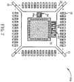
- the leadframe package 10a comprises a semiconductor die 12 that is mounted on a die pad 14 of copper or copper alloys such as C7025, A192 or the like. Likewise, a plurality of bond pads 13 are provided on a top surface of the semiconductor die 12. Some of the bond pads 13 are electrically connected to corresponding leads 16 through bond wires 18.
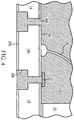
- the separate pad segment 14b does not directly contact with any of the leads 16. More specifically, the separate pad segment 14b does not need any structural support from the leads 16 or the die pad 14.
- the slit 40a between the separate pad segment 14a and the die pad 14 and the slit 40b between the separate pad segment 14b and the die pad 14 are both filled with epoxy molding compound 20.
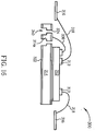
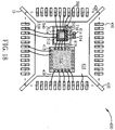
- a passive component 560 is mounted on the primary die pad 414 and the secondary die pad 514 across a slit 540 between the primary die pad 414 and the secondary die pad 514.
- Some of the bond pads 41 3 are wire bonded to respective bond pads 513 on the semiconductor die 512 through bond wires 618.
- Some of the bond pads 513 on the second semiconductor die 512 are wire bonded to the separate pad segments 614 through bond wires 718.
- the entire assembly is encapsulated or molded by a molding compound 420.
Landscapes
- Lead Frames For Integrated Circuits (AREA)
- Encapsulation Of And Coatings For Semiconductor Or Solid State Devices (AREA)
Claims (6)
- Halbleiter-Packungsprodukt, umfassend:eine Halbleitervorrichtung (12);ein Chipfeld (14) mit einem primären Bereich, einem ersten sekundären Bereich (14a) und einem zweiten sekundären Bereich (14b), wobei der primäre Bereich die Halbleitervorrichtung (12) trägt, und der erste sekundäre Bereich (14a) und der zweite sekundäre Bereich (14b) zwei Erdungsanschlüsse bereitstellen;mehrere Leiter (16) zum Kontaktieren eines Satzes von Signalleitungen, die mit der Halbleitervorrichtung (12) verdrahtet sind; undeine Vergussmasse (20) zum Einkapseln der Halbleitervorrichtung (12), des Chipfelds (14) und eines Bereichs der Leiter(16) und zum Freilegen einer Bodenseite der sekundären Bereiche (14a, 14b) des Chipfelds (14),wobei das Halbleiter-Packungsprodukt ferner eine erste Erdungssignalleitung zum Verbinden einer ersten Erdungsschaltung der Halbleitervorrichtung (12) mit dem ersten sekundären Bereich (14a) des Chipfelds (14), und eine zweite Erdungssignalleitung zum Verbinden einer zweiten Erdungsschaltung der Halbleitervorrichtung (12) mit dem zweiten sekundären Bereich (14b) des Chipfelds (14) aufweist, undwobei die Leiter (16) nicht mit dem Chipfeld (14) bündig sind.
- Halbleiter-Packungsprodukt nach Anspruch 1, wobei die erste Erdungsschaltung eine analoge Schaltung ist und die zweite Erdungsschaltung eine digitale Schaltung der Halbleitervorrichtung (12) ist.
- Halbleiter-Packungsprodukt nach Anspruch 1, wobei ein Trennbereich (40a, 40b) zwischen dem primären Bereich und einem der sekundären Bereiche (14a, 14b) einen umgekehrten T-förmigen Querschnitt aufweist und mit der Vergussmasse zum weiteren Stabilisieren des Chipfelds gefüllt ist.
- Halbleiter-Packungsprodukt nach Anspruch 1, wobei ein Trennbereich (40a, 40b) zwischen dem primären Bereich und einem der sekundären Bereiche (14a, 14b) einen sanduhrförmigen Querschnitt aufweist und mit der Vergussmasse zum weiteren Stabilisieren des Chipfelds gefüllt ist.
- Halbleiter-Packungsprodukt nach Anspruch 1, wobei ein Trennbereich (40a, 40b) zwischen dem primären Bereich und einem der sekundären Bereiche (14a, 14b) einen Abschnitt mit einer Sägezahnkante (70) aufweist.
- Halbleiter-Packungsprodukt nach Anspruch 1, wobei der erste Sekundärbereich (14a) als off-chip Induktor-Vorrichtung ausgebildet ist.
Applications Claiming Priority (1)
| Application Number | Priority Date | Filing Date | Title |
|---|---|---|---|
| US87199306P | 2006-12-27 | 2006-12-27 |
Publications (3)
| Publication Number | Publication Date |
|---|---|
| EP1944802A2 EP1944802A2 (de) | 2008-07-16 |
| EP1944802A3 EP1944802A3 (de) | 2009-03-11 |
| EP1944802B1 true EP1944802B1 (de) | 2018-02-14 |
Family
ID=39471788
Family Applications (1)
| Application Number | Title | Priority Date | Filing Date |
|---|---|---|---|
| EP07025144.2A Ceased EP1944802B1 (de) | 2006-12-27 | 2007-12-27 | Halbleiterpackung |
Country Status (3)
| Country | Link |
|---|---|
| EP (1) | EP1944802B1 (de) |
| CN (1) | CN101211794A (de) |
| TW (1) | TWI376019B (de) |
Families Citing this family (4)
| Publication number | Priority date | Publication date | Assignee | Title |
|---|---|---|---|---|
| EP2115774A2 (de) * | 2007-02-14 | 2009-11-11 | Nxp B.V. | Eingebetteter induktor und verfahren zu seiner herstellung |
| US8058720B2 (en) * | 2008-11-19 | 2011-11-15 | Mediatek Inc. | Semiconductor package |
| JP4851618B1 (ja) * | 2010-11-15 | 2012-01-11 | シャープ株式会社 | 半導体パッケージ |
| US9177834B2 (en) | 2014-02-19 | 2015-11-03 | Freescale Semiconductor, Inc. | Power bar design for lead frame-based packages |
Citations (2)
| Publication number | Priority date | Publication date | Assignee | Title |
|---|---|---|---|---|
| JPH03166755A (ja) * | 1989-11-27 | 1991-07-18 | Seiko Epson Corp | 半導体集積回路用リードフレーム |
| JPH03166756A (ja) * | 1989-11-27 | 1991-07-18 | Seiko Epson Corp | 半導体集積回路用リードフレーム |
Family Cites Families (9)
| Publication number | Priority date | Publication date | Assignee | Title |
|---|---|---|---|---|
| US6989294B1 (en) * | 1998-06-10 | 2006-01-24 | Asat, Ltd. | Leadless plastic chip carrier with etch back pad singulation |
| US6933594B2 (en) * | 1998-06-10 | 2005-08-23 | Asat Ltd. | Leadless plastic chip carrier with etch back pad singulation |
| US7005326B1 (en) * | 1998-06-24 | 2006-02-28 | Amkor Technology, Inc. | Method of making an integrated circuit package |
| US6238952B1 (en) * | 2000-02-29 | 2001-05-29 | Advanced Semiconductor Engineering, Inc. | Low-pin-count chip package and manufacturing method thereof |
| US6483178B1 (en) * | 2000-07-14 | 2002-11-19 | Siliconware Precision Industries Co., Ltd. | Semiconductor device package structure |
| SG120858A1 (en) * | 2001-08-06 | 2006-04-26 | Micron Technology Inc | Quad flat no-lead (qfn) grid array package, methodof making and memory module and computer system including same |
| US6818973B1 (en) * | 2002-09-09 | 2004-11-16 | Amkor Technology, Inc. | Exposed lead QFP package fabricated through the use of a partial saw process |
| TWI227051B (en) * | 2004-04-09 | 2005-01-21 | Airoha Tech Corp | Exposed pad module integrated a passive device therein |
| TWI245392B (en) * | 2004-06-29 | 2005-12-11 | Advanced Semiconductor Eng | Leadless semiconductor package and method for manufacturing the same |
-
2007
- 2007-12-26 CN CNA2007103011633A patent/CN101211794A/zh active Pending
- 2007-12-27 TW TW96150616A patent/TWI376019B/zh not_active IP Right Cessation
- 2007-12-27 EP EP07025144.2A patent/EP1944802B1/de not_active Ceased
Patent Citations (2)
| Publication number | Priority date | Publication date | Assignee | Title |
|---|---|---|---|---|
| JPH03166755A (ja) * | 1989-11-27 | 1991-07-18 | Seiko Epson Corp | 半導体集積回路用リードフレーム |
| JPH03166756A (ja) * | 1989-11-27 | 1991-07-18 | Seiko Epson Corp | 半導体集積回路用リードフレーム |
Also Published As
| Publication number | Publication date |
|---|---|
| EP1944802A3 (de) | 2009-03-11 |
| CN101211794A (zh) | 2008-07-02 |
| TW200828525A (en) | 2008-07-01 |
| EP1944802A2 (de) | 2008-07-16 |
| TWI376019B (en) | 2012-11-01 |
Similar Documents
| Publication | Publication Date | Title |
|---|---|---|
| US8124461B2 (en) | Method for manufacturing leadframe, packaging method for using the leadframe and semiconductor package product | |
| US7834435B2 (en) | Leadframe with extended pad segments between leads and die pad, and leadframe package using the same | |
| US8035204B2 (en) | Large die package structures and fabrication method therefor | |
| US7986032B2 (en) | Semiconductor package system with substrate having different bondable heights at lead finger tips | |
| US7646083B2 (en) | I/O connection scheme for QFN leadframe and package structures | |
| EP3147942B1 (de) | Halbleitergehäuse, halbleiterbauelement damit und herstellungsverfahren dafür | |
| TWI517333B (zh) | 具雙重連接性之積體電路封裝系統 | |
| CN102201386A (zh) | 方形扁平无引线半导体封装及其制作方法 | |
| CN101803015A (zh) | 具有弯曲外引线的半导体芯片封装 | |
| US7060536B2 (en) | Dual row leadframe and fabrication method | |
| US20040188818A1 (en) | Multi-chips module package | |
| EP1944802B1 (de) | Halbleiterpackung | |
| US7307352B2 (en) | Semiconductor package having changed substrate design using special wire bonding | |
| US7298026B2 (en) | Large die package and method for the fabrication thereof | |
| US7102241B2 (en) | Leadless semiconductor package | |
| US20060289981A1 (en) | Packaging logic and memory integrated circuits | |
| US7361984B2 (en) | Chip package structure | |
| TWI385774B (zh) | 導線架封裝及導線架 | |
| US8106502B2 (en) | Integrated circuit packaging system with plated pad and method of manufacture thereof | |
| CN101515555A (zh) | 覆晶式四方扁平无引脚型态封装结构及其制程 | |
| HK1118955B (en) | Packaging logic and memory integrated circuits |
Legal Events
| Date | Code | Title | Description |
|---|---|---|---|
| PUAI | Public reference made under article 153(3) epc to a published international application that has entered the european phase |
Free format text: ORIGINAL CODE: 0009012 |
|
| 17P | Request for examination filed |
Effective date: 20071227 |
|
| AK | Designated contracting states |
Kind code of ref document: A2 Designated state(s): AT BE BG CH CY CZ DE DK EE ES FI FR GB GR HU IE IS IT LI LT LU LV MC MT NL PL PT RO SE SI SK TR |
|
| AX | Request for extension of the european patent |
Extension state: AL BA HR MK RS |
|
| PUAL | Search report despatched |
Free format text: ORIGINAL CODE: 0009013 |
|
| AK | Designated contracting states |
Kind code of ref document: A3 Designated state(s): AT BE BG CH CY CZ DE DK EE ES FI FR GB GR HU IE IS IT LI LT LU LV MC MT NL PL PT RO SE SI SK TR |
|
| AX | Request for extension of the european patent |
Extension state: AL BA HR MK RS |
|
| AKX | Designation fees paid |
Designated state(s): DE FR GB |
|
| 17Q | First examination report despatched |
Effective date: 20091119 |
|
| RIC1 | Information provided on ipc code assigned before grant |
Ipc: H01L 23/66 20060101ALI20170801BHEP Ipc: H01L 21/48 20060101ALI20170801BHEP Ipc: H01L 25/10 20060101ALI20170801BHEP Ipc: H01L 23/50 20060101ALI20170801BHEP Ipc: H01L 25/16 20060101ALN20170801BHEP Ipc: H01L 23/31 20060101ALI20170801BHEP Ipc: H01L 23/495 20060101AFI20170801BHEP Ipc: H01L 23/00 20060101ALI20170801BHEP |
|
| RIC1 | Information provided on ipc code assigned before grant |
Ipc: H01L 23/66 20060101ALI20170828BHEP Ipc: H01L 25/10 20060101ALI20170828BHEP Ipc: H01L 23/00 20060101ALI20170828BHEP Ipc: H01L 23/31 20060101ALI20170828BHEP Ipc: H01L 21/48 20060101ALI20170828BHEP Ipc: H01L 25/16 20060101ALN20170828BHEP Ipc: H01L 23/50 20060101ALI20170828BHEP Ipc: H01L 23/495 20060101AFI20170828BHEP |
|
| GRAP | Despatch of communication of intention to grant a patent |
Free format text: ORIGINAL CODE: EPIDOSNIGR1 |
|
| INTG | Intention to grant announced |
Effective date: 20171009 |
|
| GRAS | Grant fee paid |
Free format text: ORIGINAL CODE: EPIDOSNIGR3 |
|
| GRAA | (expected) grant |
Free format text: ORIGINAL CODE: 0009210 |
|
| AK | Designated contracting states |
Kind code of ref document: B1 Designated state(s): DE FR GB |
|
| REG | Reference to a national code |
Ref country code: GB Ref legal event code: FG4D |
|
| REG | Reference to a national code |
Ref country code: DE Ref legal event code: R096 Ref document number: 602007053909 Country of ref document: DE |
|
| REG | Reference to a national code |
Ref country code: DE Ref legal event code: R097 Ref document number: 602007053909 Country of ref document: DE |
|
| PLBE | No opposition filed within time limit |
Free format text: ORIGINAL CODE: 0009261 |
|
| STAA | Information on the status of an ep patent application or granted ep patent |
Free format text: STATUS: NO OPPOSITION FILED WITHIN TIME LIMIT |
|
| 26N | No opposition filed |
Effective date: 20181115 |
|
| P01 | Opt-out of the competence of the unified patent court (upc) registered |
Effective date: 20230607 |
|
| PGFP | Annual fee paid to national office [announced via postgrant information from national office to epo] |
Ref country code: GB Payment date: 20231227 Year of fee payment: 17 |
|
| PGFP | Annual fee paid to national office [announced via postgrant information from national office to epo] |
Ref country code: FR Payment date: 20231227 Year of fee payment: 17 |
|
| PGFP | Annual fee paid to national office [announced via postgrant information from national office to epo] |
Ref country code: DE Payment date: 20231229 Year of fee payment: 17 |
|
| REG | Reference to a national code |
Ref country code: DE Ref legal event code: R119 Ref document number: 602007053909 Country of ref document: DE |
|
| GBPC | Gb: european patent ceased through non-payment of renewal fee |
Effective date: 20241227 |
|
| PG25 | Lapsed in a contracting state [announced via postgrant information from national office to epo] |
Ref country code: DE Free format text: LAPSE BECAUSE OF NON-PAYMENT OF DUE FEES Effective date: 20250701 |
|
| PG25 | Lapsed in a contracting state [announced via postgrant information from national office to epo] |
Ref country code: GB Free format text: LAPSE BECAUSE OF NON-PAYMENT OF DUE FEES Effective date: 20241227 |
|
| PG25 | Lapsed in a contracting state [announced via postgrant information from national office to epo] |
Ref country code: FR Free format text: LAPSE BECAUSE OF NON-PAYMENT OF DUE FEES Effective date: 20241231 |