EP1937471B1 - Mehrschichtkörper sowie verfahren zu dessen herstellung - Google Patents
Mehrschichtkörper sowie verfahren zu dessen herstellung Download PDFInfo
- Publication number
- EP1937471B1 EP1937471B1 EP06776694.9A EP06776694A EP1937471B1 EP 1937471 B1 EP1937471 B1 EP 1937471B1 EP 06776694 A EP06776694 A EP 06776694A EP 1937471 B1 EP1937471 B1 EP 1937471B1
- Authority
- EP
- European Patent Office
- Prior art keywords
- layer
- surface structure
- region
- multilayer body
- metallic layer
- Prior art date
- Legal status (The legal status is an assumption and is not a legal conclusion. Google has not performed a legal analysis and makes no representation as to the accuracy of the status listed.)
- Active
Links
- 238000004519 manufacturing process Methods 0.000 title claims description 14
- 230000010076 replication Effects 0.000 claims description 53
- 238000000034 method Methods 0.000 claims description 22
- 229920002120 photoresistant polymer Polymers 0.000 claims description 22
- 230000003287 optical effect Effects 0.000 claims description 19
- 230000005540 biological transmission Effects 0.000 claims description 16
- 238000005406 washing Methods 0.000 claims description 15
- 238000005530 etching Methods 0.000 claims description 14
- 230000005855 radiation Effects 0.000 claims description 7
- 230000036961 partial effect Effects 0.000 claims description 6
- 238000012546 transfer Methods 0.000 claims description 6
- 239000000463 material Substances 0.000 claims description 4
- 239000002086 nanomaterial Substances 0.000 claims description 2
- 230000000873 masking effect Effects 0.000 claims 1
- 238000001429 visible spectrum Methods 0.000 claims 1
- 239000010410 layer Substances 0.000 description 238
- 239000010408 film Substances 0.000 description 35
- 229910052751 metal Inorganic materials 0.000 description 20
- 239000002184 metal Substances 0.000 description 20
- 230000000694 effects Effects 0.000 description 19
- 239000011888 foil Substances 0.000 description 8
- 229910052709 silver Inorganic materials 0.000 description 8
- 239000012790 adhesive layer Substances 0.000 description 7
- 239000010931 gold Substances 0.000 description 7
- BQCADISMDOOEFD-UHFFFAOYSA-N Silver Chemical compound [Ag] BQCADISMDOOEFD-UHFFFAOYSA-N 0.000 description 6
- 229910052782 aluminium Inorganic materials 0.000 description 6
- 229910052737 gold Inorganic materials 0.000 description 6
- 239000004332 silver Substances 0.000 description 6
- XAGFODPZIPBFFR-UHFFFAOYSA-N aluminium Chemical compound [Al] XAGFODPZIPBFFR-UHFFFAOYSA-N 0.000 description 5
- 230000001419 dependent effect Effects 0.000 description 5
- 238000013461 design Methods 0.000 description 5
- 238000001000 micrograph Methods 0.000 description 5
- 230000015572 biosynthetic process Effects 0.000 description 4
- 239000011651 chromium Substances 0.000 description 4
- 239000010949 copper Substances 0.000 description 4
- 230000005670 electromagnetic radiation Effects 0.000 description 4
- PCHJSUWPFVWCPO-UHFFFAOYSA-N gold Chemical compound [Au] PCHJSUWPFVWCPO-UHFFFAOYSA-N 0.000 description 4
- 150000002739 metals Chemical group 0.000 description 4
- 230000000737 periodic effect Effects 0.000 description 4
- 230000003068 static effect Effects 0.000 description 4
- RYGMFSIKBFXOCR-UHFFFAOYSA-N Copper Chemical compound [Cu] RYGMFSIKBFXOCR-UHFFFAOYSA-N 0.000 description 3
- 230000015556 catabolic process Effects 0.000 description 3
- 229910052804 chromium Inorganic materials 0.000 description 3
- 229910052802 copper Inorganic materials 0.000 description 3
- 238000011161 development Methods 0.000 description 3
- 238000004806 packaging method and process Methods 0.000 description 3
- 238000012216 screening Methods 0.000 description 3
- 230000000007 visual effect Effects 0.000 description 3
- VYZAMTAEIAYCRO-UHFFFAOYSA-N Chromium Chemical compound [Cr] VYZAMTAEIAYCRO-UHFFFAOYSA-N 0.000 description 2
- KDLHZDBZIXYQEI-UHFFFAOYSA-N Palladium Chemical compound [Pd] KDLHZDBZIXYQEI-UHFFFAOYSA-N 0.000 description 2
- 239000004020 conductor Substances 0.000 description 2
- 230000007423 decrease Effects 0.000 description 2
- 239000004922 lacquer Substances 0.000 description 2
- 229910001092 metal group alloy Inorganic materials 0.000 description 2
- 229910052760 oxygen Inorganic materials 0.000 description 2
- 239000001301 oxygen Substances 0.000 description 2
- 239000000758 substrate Substances 0.000 description 2
- 238000012795 verification Methods 0.000 description 2
- OKTJSMMVPCPJKN-UHFFFAOYSA-N Carbon Chemical compound [C] OKTJSMMVPCPJKN-UHFFFAOYSA-N 0.000 description 1
- MYMOFIZGZYHOMD-UHFFFAOYSA-N Dioxygen Chemical compound O=O MYMOFIZGZYHOMD-UHFFFAOYSA-N 0.000 description 1
- 240000005702 Galium aparine Species 0.000 description 1
- 239000004831 Hot glue Substances 0.000 description 1
- 238000003848 UV Light-Curing Methods 0.000 description 1
- 238000002679 ablation Methods 0.000 description 1
- 238000010521 absorption reaction Methods 0.000 description 1
- 230000002730 additional effect Effects 0.000 description 1
- 239000000853 adhesive Substances 0.000 description 1
- 230000001070 adhesive effect Effects 0.000 description 1
- 229910045601 alloy Inorganic materials 0.000 description 1
- 239000000956 alloy Substances 0.000 description 1
- 238000000149 argon plasma sintering Methods 0.000 description 1
- QVGXLLKOCUKJST-UHFFFAOYSA-N atomic oxygen Chemical compound [O] QVGXLLKOCUKJST-UHFFFAOYSA-N 0.000 description 1
- 230000002238 attenuated effect Effects 0.000 description 1
- 229910052799 carbon Inorganic materials 0.000 description 1
- 238000000576 coating method Methods 0.000 description 1
- 230000001427 coherent effect Effects 0.000 description 1
- 239000003086 colorant Substances 0.000 description 1
- 239000002131 composite material Substances 0.000 description 1
- 238000005034 decoration Methods 0.000 description 1
- 239000000975 dye Substances 0.000 description 1
- 230000005672 electromagnetic field Effects 0.000 description 1
- 238000011156 evaluation Methods 0.000 description 1
- 230000005284 excitation Effects 0.000 description 1
- 238000002474 experimental method Methods 0.000 description 1
- 239000011521 glass Substances 0.000 description 1
- 238000007646 gravure printing Methods 0.000 description 1
- 238000010438 heat treatment Methods 0.000 description 1
- 238000003384 imaging method Methods 0.000 description 1
- 238000001746 injection moulding Methods 0.000 description 1
- 239000012212 insulator Substances 0.000 description 1
- 239000002346 layers by function Substances 0.000 description 1
- 239000007788 liquid Substances 0.000 description 1
- 239000002932 luster Substances 0.000 description 1
- 239000011104 metalized film Substances 0.000 description 1
- 238000001465 metallisation Methods 0.000 description 1
- 230000003278 mimic effect Effects 0.000 description 1
- 239000012044 organic layer Substances 0.000 description 1
- 239000012785 packaging film Substances 0.000 description 1
- 229920006280 packaging film Polymers 0.000 description 1
- 229910052763 palladium Inorganic materials 0.000 description 1
- 238000000059 patterning Methods 0.000 description 1
- 239000002985 plastic film Substances 0.000 description 1
- 229920006255 plastic film Polymers 0.000 description 1
- 230000010287 polarization Effects 0.000 description 1
- 150000003071 polychlorinated biphenyls Chemical class 0.000 description 1
- 229920006267 polyester film Polymers 0.000 description 1
- 229920000642 polymer Polymers 0.000 description 1
- 238000007639 printing Methods 0.000 description 1
- 230000001681 protective effect Effects 0.000 description 1
- 230000002829 reductive effect Effects 0.000 description 1
- 238000002310 reflectometry Methods 0.000 description 1
- 230000003362 replicative effect Effects 0.000 description 1
- 239000004065 semiconductor Substances 0.000 description 1
- 238000001228 spectrum Methods 0.000 description 1
- 239000000126 substance Substances 0.000 description 1
- 230000001502 supplementing effect Effects 0.000 description 1
- 210000004243 sweat Anatomy 0.000 description 1
- 238000012360 testing method Methods 0.000 description 1
- 229920001169 thermoplastic Polymers 0.000 description 1
- 239000004416 thermosoftening plastic Substances 0.000 description 1
- 229910052719 titanium Inorganic materials 0.000 description 1
- 239000010936 titanium Substances 0.000 description 1
- 238000007740 vapor deposition Methods 0.000 description 1
- 230000004304 visual acuity Effects 0.000 description 1
- XLYOFNOQVPJJNP-UHFFFAOYSA-N water Substances O XLYOFNOQVPJJNP-UHFFFAOYSA-N 0.000 description 1
Images


Classifications
-
- B—PERFORMING OPERATIONS; TRANSPORTING
- B32—LAYERED PRODUCTS
- B32B—LAYERED PRODUCTS, i.e. PRODUCTS BUILT-UP OF STRATA OF FLAT OR NON-FLAT, e.g. CELLULAR OR HONEYCOMB, FORM
- B32B15/00—Layered products comprising a layer of metal
- B32B15/04—Layered products comprising a layer of metal comprising metal as the main or only constituent of a layer, which is next to another layer of the same or of a different material
- B32B15/08—Layered products comprising a layer of metal comprising metal as the main or only constituent of a layer, which is next to another layer of the same or of a different material of synthetic resin
-
- B—PERFORMING OPERATIONS; TRANSPORTING
- B42—BOOKBINDING; ALBUMS; FILES; SPECIAL PRINTED MATTER
- B42D—BOOKS; BOOK COVERS; LOOSE LEAVES; PRINTED MATTER CHARACTERISED BY IDENTIFICATION OR SECURITY FEATURES; PRINTED MATTER OF SPECIAL FORMAT OR STYLE NOT OTHERWISE PROVIDED FOR; DEVICES FOR USE THEREWITH AND NOT OTHERWISE PROVIDED FOR; MOVABLE-STRIP WRITING OR READING APPARATUS
- B42D25/00—Information-bearing cards or sheet-like structures characterised by identification or security features; Manufacture thereof
- B42D25/30—Identification or security features, e.g. for preventing forgery
- B42D25/36—Identification or security features, e.g. for preventing forgery comprising special materials
- B42D25/373—Metallic materials
-
- B—PERFORMING OPERATIONS; TRANSPORTING
- B42—BOOKBINDING; ALBUMS; FILES; SPECIAL PRINTED MATTER
- B42D—BOOKS; BOOK COVERS; LOOSE LEAVES; PRINTED MATTER CHARACTERISED BY IDENTIFICATION OR SECURITY FEATURES; PRINTED MATTER OF SPECIAL FORMAT OR STYLE NOT OTHERWISE PROVIDED FOR; DEVICES FOR USE THEREWITH AND NOT OTHERWISE PROVIDED FOR; MOVABLE-STRIP WRITING OR READING APPARATUS
- B42D25/00—Information-bearing cards or sheet-like structures characterised by identification or security features; Manufacture thereof
- B42D25/30—Identification or security features, e.g. for preventing forgery
- B42D25/324—Reliefs
-
- B—PERFORMING OPERATIONS; TRANSPORTING
- B42—BOOKBINDING; ALBUMS; FILES; SPECIAL PRINTED MATTER
- B42D—BOOKS; BOOK COVERS; LOOSE LEAVES; PRINTED MATTER CHARACTERISED BY IDENTIFICATION OR SECURITY FEATURES; PRINTED MATTER OF SPECIAL FORMAT OR STYLE NOT OTHERWISE PROVIDED FOR; DEVICES FOR USE THEREWITH AND NOT OTHERWISE PROVIDED FOR; MOVABLE-STRIP WRITING OR READING APPARATUS
- B42D25/00—Information-bearing cards or sheet-like structures characterised by identification or security features; Manufacture thereof
- B42D25/30—Identification or security features, e.g. for preventing forgery
- B42D25/328—Diffraction gratings; Holograms
-
- B—PERFORMING OPERATIONS; TRANSPORTING
- B42—BOOKBINDING; ALBUMS; FILES; SPECIAL PRINTED MATTER
- B42D—BOOKS; BOOK COVERS; LOOSE LEAVES; PRINTED MATTER CHARACTERISED BY IDENTIFICATION OR SECURITY FEATURES; PRINTED MATTER OF SPECIAL FORMAT OR STYLE NOT OTHERWISE PROVIDED FOR; DEVICES FOR USE THEREWITH AND NOT OTHERWISE PROVIDED FOR; MOVABLE-STRIP WRITING OR READING APPARATUS
- B42D25/00—Information-bearing cards or sheet-like structures characterised by identification or security features; Manufacture thereof
- B42D25/40—Manufacture
- B42D25/405—Marking
- B42D25/415—Marking using chemicals
- B42D25/42—Marking using chemicals by photographic processes
-
- B—PERFORMING OPERATIONS; TRANSPORTING
- B42—BOOKBINDING; ALBUMS; FILES; SPECIAL PRINTED MATTER
- B42D—BOOKS; BOOK COVERS; LOOSE LEAVES; PRINTED MATTER CHARACTERISED BY IDENTIFICATION OR SECURITY FEATURES; PRINTED MATTER OF SPECIAL FORMAT OR STYLE NOT OTHERWISE PROVIDED FOR; DEVICES FOR USE THEREWITH AND NOT OTHERWISE PROVIDED FOR; MOVABLE-STRIP WRITING OR READING APPARATUS
- B42D25/00—Information-bearing cards or sheet-like structures characterised by identification or security features; Manufacture thereof
- B42D25/40—Manufacture
- B42D25/45—Associating two or more layers
-
- B—PERFORMING OPERATIONS; TRANSPORTING
- B44—DECORATIVE ARTS
- B44C—PRODUCING DECORATIVE EFFECTS; MOSAICS; TARSIA WORK; PAPERHANGING
- B44C1/00—Processes, not specifically provided for elsewhere, for producing decorative surface effects
- B44C1/16—Processes, not specifically provided for elsewhere, for producing decorative surface effects for applying transfer pictures or the like
- B44C1/165—Processes, not specifically provided for elsewhere, for producing decorative surface effects for applying transfer pictures or the like for decalcomanias; sheet material therefor
- B44C1/17—Dry transfer
- B44C1/1712—Decalcomanias applied under heat and pressure, e.g. provided with a heat activable adhesive
- B44C1/1716—Decalcomanias provided with a particular decorative layer, e.g. specially adapted to allow the formation of a metallic or dyestuff layer on a substrate unsuitable for direct deposition
-
- G—PHYSICS
- G03—PHOTOGRAPHY; CINEMATOGRAPHY; ANALOGOUS TECHNIQUES USING WAVES OTHER THAN OPTICAL WAVES; ELECTROGRAPHY; HOLOGRAPHY
- G03H—HOLOGRAPHIC PROCESSES OR APPARATUS
- G03H1/00—Holographic processes or apparatus using light, infrared or ultraviolet waves for obtaining holograms or for obtaining an image from them; Details peculiar thereto
- G03H1/0005—Adaptation of holography to specific applications
- G03H1/0011—Adaptation of holography to specific applications for security or authentication
-
- G—PHYSICS
- G03—PHOTOGRAPHY; CINEMATOGRAPHY; ANALOGOUS TECHNIQUES USING WAVES OTHER THAN OPTICAL WAVES; ELECTROGRAPHY; HOLOGRAPHY
- G03H—HOLOGRAPHIC PROCESSES OR APPARATUS
- G03H1/00—Holographic processes or apparatus using light, infrared or ultraviolet waves for obtaining holograms or for obtaining an image from them; Details peculiar thereto
- G03H1/02—Details of features involved during the holographic process; Replication of holograms without interference recording
- G03H1/0236—Form or shape of the hologram when not registered to the substrate, e.g. trimming the hologram to alphanumerical shape
-
- G—PHYSICS
- G03—PHOTOGRAPHY; CINEMATOGRAPHY; ANALOGOUS TECHNIQUES USING WAVES OTHER THAN OPTICAL WAVES; ELECTROGRAPHY; HOLOGRAPHY
- G03H—HOLOGRAPHIC PROCESSES OR APPARATUS
- G03H1/00—Holographic processes or apparatus using light, infrared or ultraviolet waves for obtaining holograms or for obtaining an image from them; Details peculiar thereto
- G03H1/02—Details of features involved during the holographic process; Replication of holograms without interference recording
- G03H1/0252—Laminate comprising a hologram layer
-
- H—ELECTRICITY
- H05—ELECTRIC TECHNIQUES NOT OTHERWISE PROVIDED FOR
- H05K—PRINTED CIRCUITS; CASINGS OR CONSTRUCTIONAL DETAILS OF ELECTRIC APPARATUS; MANUFACTURE OF ASSEMBLAGES OF ELECTRICAL COMPONENTS
- H05K5/00—Casings, cabinets or drawers for electric apparatus
- H05K5/02—Details
- H05K5/0217—Mechanical details of casings
- H05K5/0243—Mechanical details of casings for decorative purposes
-
- B42D2033/10—
-
- G—PHYSICS
- G03—PHOTOGRAPHY; CINEMATOGRAPHY; ANALOGOUS TECHNIQUES USING WAVES OTHER THAN OPTICAL WAVES; ELECTROGRAPHY; HOLOGRAPHY
- G03H—HOLOGRAPHIC PROCESSES OR APPARATUS
- G03H1/00—Holographic processes or apparatus using light, infrared or ultraviolet waves for obtaining holograms or for obtaining an image from them; Details peculiar thereto
- G03H1/02—Details of features involved during the holographic process; Replication of holograms without interference recording
- G03H1/024—Hologram nature or properties
- G03H1/0244—Surface relief holograms
-
- G—PHYSICS
- G03—PHOTOGRAPHY; CINEMATOGRAPHY; ANALOGOUS TECHNIQUES USING WAVES OTHER THAN OPTICAL WAVES; ELECTROGRAPHY; HOLOGRAPHY
- G03H—HOLOGRAPHIC PROCESSES OR APPARATUS
- G03H1/00—Holographic processes or apparatus using light, infrared or ultraviolet waves for obtaining holograms or for obtaining an image from them; Details peculiar thereto
- G03H1/04—Processes or apparatus for producing holograms
- G03H1/18—Particular processing of hologram record carriers, e.g. for obtaining blazed holograms
- G03H2001/187—Trimming process, i.e. macroscopically patterning the hologram
- G03H2001/188—Demetallisation, i.e. removing the enhancing metallic layer
-
- G—PHYSICS
- G03—PHOTOGRAPHY; CINEMATOGRAPHY; ANALOGOUS TECHNIQUES USING WAVES OTHER THAN OPTICAL WAVES; ELECTROGRAPHY; HOLOGRAPHY
- G03H—HOLOGRAPHIC PROCESSES OR APPARATUS
- G03H2250/00—Laminate comprising a hologram layer
- G03H2250/10—Laminate comprising a hologram layer arranged to be transferred onto a carrier body
-
- Y—GENERAL TAGGING OF NEW TECHNOLOGICAL DEVELOPMENTS; GENERAL TAGGING OF CROSS-SECTIONAL TECHNOLOGIES SPANNING OVER SEVERAL SECTIONS OF THE IPC; TECHNICAL SUBJECTS COVERED BY FORMER USPC CROSS-REFERENCE ART COLLECTIONS [XRACs] AND DIGESTS
- Y10—TECHNICAL SUBJECTS COVERED BY FORMER USPC
- Y10T—TECHNICAL SUBJECTS COVERED BY FORMER US CLASSIFICATION
- Y10T428/00—Stock material or miscellaneous articles
- Y10T428/24—Structurally defined web or sheet [e.g., overall dimension, etc.]
- Y10T428/24802—Discontinuous or differential coating, impregnation or bond [e.g., artwork, printing, retouched photograph, etc.]
Definitions
- the invention relates to a multilayer body having a replication layer which has microscopically fine pattern areas, and to a method for producing a multilayer body having adjustable or defined electrical conductivity.
- metallized multilayer bodies in particular metallized films, which have a reflective or matt or otherwise structured surface which is electrically conductive.
- the electrically conductive surface may be troublesome, for example when the foils are intended to decorate enclosures of electronic equipment, or when the foils are to serve as packaging for food exposed to the electromagnetic radiation of a microwave oven.
- Such packaging can also contain security features with a metallic surface, which can also be thermally destroyed by microwave radiation.
- the invention is based on the object of specifying a multi-layer body with adjustable or defined electrical conductivity and a manufacturing method that is cost-effective and suitable for mass production.
- the object of the invention is achieved with a method for producing a multilayer body with adjustable or defined electrical conductivity, wherein it is provided that in a first region of a replication layer of the multilayer body, a diffractive first surface structure is formed, that a metallic layer on the replication in the first region and in a second region in which the first surface structure is not formed in the replication layer, wherein either the first region or the second region is formed by a plurality of microscopically fine pattern areas, in a line grid or in a surface grid with the Rastenrveite D are arranged and which are each separated by the, each of the sub-areas completely delimiting or enclosing the second area or first area separated from each other at a distance B from each other that on the metallic layer a photoemp is applied sensitive layer or as a replication layer, a photosensitive wash mask is applied, that the photosensitive layer or wash mask is exposed through the metallic layer, so that the photosensitive layer or washing mask is exposed differently by the first surface structure in the first and in the second region and that
- the object is further achieved with a multi-layer body, in particular a transfer film, with a replication layer and a metallic layer arranged on the replication layer, wherein it is provided that the multi-layer body has a multiplicity of microscopically fine pattern areas and a background area completely delimiting or enclosing the pattern areas the pattern areas are arranged in a line grid or in an area grid with the screen width D, the pattern areas are separated from each other by the background area at a distance B from one another, the screen pitch D is smaller than 500 ⁇ m, and the ratio of the grid spacing D to the distance B in FIG Range of 5 to 200, and that the metallic layer is removed either in the background area or in the pattern areas.
- the multi-layer body has a multiplicity of microscopically fine pattern areas and a background area completely delimiting or enclosing the pattern areas the pattern areas are arranged in a line grid or in an area grid with the screen width D, the pattern areas are separated from each other by the background area at a distance B from one another, the screen pitch
- the metallic layer applied to the surface structure itself forms an optical exposure mask, the optical effect of the metallic layer being determined by the surface structure on which it is arranged.
- in-register partial removal of the metallic layer itself acting as an exposure mask can be achieved, in the high resolution and quality required to fabricate the microscopically fine island structures.
- grid is not only used here as a uniform subdivision of a surface. Rather, uneven or random grids, such as frequency-modulated grids, as used in the printing industry, understood by "raster". Thus, it is expressly included subdivisions of the area in island areas, which are formed completely stochastic.
- the lines between the island areas can also be curved and / or be of varying thickness.
- the grid width D and / or the distance B can also be average values of the totality.
- they can be line grids, ie one-dimensional grids or multi-dimensional grids, for example area grids.
- the invention thus provides a production method for partially metallized multilayer bodies, in particular partially metallized foils with microscopically fine island structures, which is particularly effective and inexpensive.
- the metallic layer of a multilayer body according to the invention which is provided with the above-specified arrangement of metallized island-shaped pattern areas, appears to the unarmed human eye as a homogeneous metallic surface.
- the metallic layer is electrically non-conductive, but throughout for electromagnetic radiation up to the microwave range.
- the multilayer body can therefore be exposed to, for example, the radiation of a microwave without noticeably heating.
- a metallically appearing, but electrically non-conductive surface can be realized.
- the effect of the electrical conductivity can be made frequency-dependent. This means that depending on the excitation frequency, an electrical conductivity may or may not be present.
- a multilayer body formed as a film is perceived as a metallic mirror film.
- Such a film can be used, for example, for the decoration of electrical appliances, such as television receivers, which are to have an electrically non-conductive surface.
- a transparent film having an electrically conductive surface can be produced.
- Such an electrically conductive film may have, for example, demetallized pattern areas which are surrounded by a metallized background area.
- This film can be used, for example, as a transparent shielding film, which despite its transparency because of the reticulated metallized background region to shield electromagnetic radiation or is able to dissipate static electrical charges.
- Any electrical conductivities can be adjusted, for example, by varying the layer thickness of the metallic layer or by varying the ratio D / B.
- a multilayer body may be formed as a film which is insulating in one direction and conducting in another direction.
- the screen width D is selected in the range of 1 .mu.m to 500 .mu.m, preferably in the range of 5 .mu.m to 300 .mu.m. It can also be provided that the grid width in the range from 10 ⁇ m to 250 ⁇ m. If the screen width D is in these ranges, conspicuous diffraction effects of the multilayer body are avoided on the one hand, and on the other hand the pattern areas are not visible in detail since the subdivision lies below the resolution limit of the unarmed human eye.
- the ratio of the grid width D to the distance B in the range of 5 to 200 is selected.
- the ratio D / B in particular the electrical breakdown strength of the multilayer body can be influenced.
- the metallic layer is applied to a plane spanned by the replication layer over its entire surface in a constant areal density, preferably vapor-deposited.
- Such a method is inexpensive and well controllable in the layer thickness of the metallic layer.
- the metallic layer is applied to the replication completely over the entire surface in a thickness at which the metallic layer has an optical density of between 1 and 7 in a region of the replication layer without a surface structure.
- the effect of the different transmission, in particular transparency, is set by the depth-to-width ratio of the surface structure of the replication layer described in more detail below.
- the metallic layer may be a metal, for example aluminum, silver, gold, copper, chromium or palladium, or an alloy of these and / or other metals, or a layer sequence of the metals listed above.
- the transmission in particular the transparency of the metallic layer in the first region relative to the transmission, in particular, increases the transparency of the metallic layer in the second region, or vice versa.
- the transmission, in particular the transparency, or the optical density of the metallic layer can thus be influenced by means of the surface structure in the replication layer. Even slight differences in transmission or transparency, which are no longer perceptible, for example, by the human eye, may be sufficient under suitable production conditions to use the metallic layer as an exposure mask. Because the replication layer can be inexpensively formed with a very fine surface structure, the required high resolutions in the partial demetallization of the metallic layer can also be carried out inexpensively.
- the first surface structure has a greater relief depth than the second surface structure or vice versa.
- the product of Spatialfrequenz and relief depth of the first surface structure is greater than the product of Spatialfrequenz and relief depth of the second surface structure or vice versa.
- the spatial frequency is given in lines / mm and is a characteristic feature of diffractive structures. In the preferred screen width of 5 microns to 300 microns, it is advantageously chosen between 500 lines / mm and 5000 lines / mm. In structures with stochastic profile, such as matte structures, is a typical characteristic Distance between surveys used or, for example, the so-called correlation length. This parameter is analogously between 0.2 and 2.0 microns.
- a surface structure having a high depth-to-width ratio of the individual structural elements, in particular with a depth-to-width ratio> 0.3 is molded and that the second surface structure is formed as a surface structure with a lower depth-to-width ratio, or vice versa.
- the dimensionless depth-to-width ratio is a characteristic feature of surface enlargement by preferably periodic structures.
- Such a structure forms “mountains” and “valleys” in a periodic sequence.
- Depth is here the distance between “mountain” and “valley”, as width the distance between two “mountains”.
- This effect can also be observed in the case of discretely distributed "valleys", which can be arranged at a distance that is many times greater than the depth of the "valleys".
- the depth of the "valley” should be related to the width of the "valley” to properly describe the geometry of the "valley” by specifying the depth-to-width ratio.
- a photosensitive material having a binary characteristic is applied as the photosensitive layer or as a photosensitive wash mask and that the photosensitive layer or the photosensitive wash mask is exposed through the metallic layer in an exposure intensity and exposure time such that the photosensitive layer or photosensitive layer is exposed the photosensitive washing mask in the first region or in the second region, in which the transmission, in particular the transparency of the metallic layer is conditionally increased by the first surface structure, is activated and is not activated in the second region, or vice versa.
- UV radiation is more energetic than daylight and therefore often preferred.
- the areas of the photosensitive washing mask activated by the exposure and the areas of the metallic layer arranged thereon can be removed in a washing process.
- the exposed photosensitive layer is developed and that the developed photosensitive layer forms an etching mask for the metallic layer.
- a further advantageous embodiment provides that the photosensitive layer is activated by the exposure in the first region in which the transmission, in particular the transparency of the metallic layer is increased by the first surface structure, and that the activated photoactivatable layer is an etchant for the metallic Layer forms.
- the photosensitive layer is formed of a photoresist.
- the photoresist may be formed as a positive photoresist or as a negative photoresist.
- the photosensitive layer may also be a photopolymer.
- the exposure takes place in each case on the photoresist side, but it can also take place through the metallic layer.
- the structuring can also be done by direct laser irradiation (ablation), without the detour using photoresist as "amplifier".
- absorption irradiation
- photoresist as "amplifier”.
- the structuring can take place by utilizing the structure-dependent etching behavior of the metallic layer. Namely, if patterned surfaces are vapor-deposited with a metallic layer and exposed to a suitable etching medium, high aspect ratio regions appear transparent after a certain time, while unstructured regions or low aspect ratio regions still appear largely opaque. Such a time-controlled etching process ends, for example, when in regions of the replication layer with surface relief structure and effectively thinner layer thickness of the metallic layer transparency was generated, while in regions of the replication without surface structure and effectively thicker layer thickness of the metallic layer still opaque metallic layer is present.
- the etching of the metallic layer which also occurs in the unstructured regions is usually precompensated by an initially increased optical density of the vapor-deposited metallic layer.
- the formation of a mobile phone housing may be provided.
- the combination may be provided with classical demetallization. It can therefore be provided that further areas are demetallized completely or partially by classical demetallization.
- one or more layers of the multilayer body can be colored to produce a visual impression.
- the multilayer body may furthermore comprise at least one transparent or opaque colored layer formed over the whole area or partially. It is particularly preferred if the at least one colored layer is formed in register with the metallic layer, in particular in the first or second region free of the metallic layer. As a result, a colored impression can be achieved and / or the multilayer body can be made opaque despite the partial metallization.
- the at least one colored layer is arranged in the first or second region free of the metallic layer and furthermore has a color similar to the metallic layer. For example, in the case of a silver metallic layer, a gray or, in the case of a golden metallic layer, a yellowish layer is preferred which helps to suggest to the human eye a reflective metallic layer without interruptions.
- the at least one colored layer is formed either as an electrically conductive layer, which contains, for example, non-metallic electrically conductive substances, such as carbon or polymers, or as an electrically insulating layer, which, for example, increases the breakdown voltage .
- the at least one colored layer can also be a semiconducting layer.
- the at least one colored layer contains no metal.
- CMYK complementary metal-oxide-semiconductor
- dyes which are opaque or transparent only in a certain wavelength range and which act as filters, for example when exposed to UV light. This can be achieved by pressure additional local structuring of the conductivity, which can also be influenced by the choice of the spectrum of the light source.
- the metallic layer is galvanically reinforced. It is also possible to reinforce the layer by a second metal or a metal alloy. After exposure, the photoresist is partially removed so that corresponding metallic areas of the metallic layer are exposed. The galvanic structure now takes place in the exposed areas, while the photoresist-covered areas essentially serve to ensure the necessary electrical conductivity for the galvanic structure. Subsequently, the photoresist is also removed from these areas. The remaining thin metallic layer in the background area becomes then removed by etching.
- the grid is formed with a constant screen width D.
- the grid is formed with a non-constant grid width D.
- the screen width D preferably varies randomly over a range of ⁇ 40%. With such a randomized variation of the screen ruling, the occurrence of moire can be counteracted, and diffraction effects can be avoided, which may occur in the case of screens having a constant screen ruling. can make disturbing noticeable.
- the first or second surface structure may be formed as an optically active, reflective or transmitting light-diffractive and / or refractive and / or light-scattering microstructure or nanostructure, for example as a lattice structure, such as a linear lattice or a lattice, as a superposition of a plurality of lattice structures, as an isotropic or anisotropic matt structure, as binary or continuous Fresnel lens, as a microprism, as Blazegitter, as a combination structure or as a macrostructure.
- a lattice structure such as a linear lattice or a lattice, as a superposition of a plurality of lattice structures, as an isotropic or anisotropic matt structure, as binary or continuous Fresnel lens, as a microprism, as Blazegitter, as a combination structure or as a macrostructure.
- a lattice structure such as a linear lattice
- the reflectivity is only slightly reduced by the partial demetallization, so that the hologram is perceived at substantially the same intensity as an electrically conductive version. Because the Rasttation is below the resolution limit of the unaided eye, it remains hidden from the human observer, if the screening is chosen such that no moiré effects occur with design elements of the hologram. Even with machine evaluation no quality losses are to be feared.
- the transmission behavior of the non-conductive mirror foil can be changed clearly recognizable, while the reflection behavior varies only imperceptibly. When viewed in reflected light, therefore, no information is visible, while it opens up when viewed in transmitted light, for example, as a pictorial representation.
- the multilayer body has a second metallic layer, which is arranged in register with a first metallic layer and / or the at least one colored layer.
- the metallic layers may have different thicknesses, as a result of which, on the one hand, the electrical properties of the multi-layer body and, on the other hand, the optical properties of the multi-layer body can be designed further.
- At least one of the metallic layers is applied in a layer thickness in which it is partially transparent in the visible range.
- the layer thickness to be selected depends on the material. Layer thicknesses of a few 10 nm can already appear opaque, ie non-transparent. For example, aluminum appears opaque when its optical density is in the range of 1 to 5. It is further determined by the depth-to-width ratio of the surface structure of the replication layer on which the metallic layer is deposited.
- the metallic layer may still have an electrical conductivity which is sufficient for many applications. It can be provided, for example, to use such a film designed as a multilayer body for shielding electromagnetic radiation or for dissipating static electrical charges.
- the multilayer body can thus u.a. be used as a packaging film for static-sensitive components such as microprocessors. It can also be provided that such a film is formed only with a metallic layer, as described above.
- the distance between the metallic layers is chosen such that interference effects occur.
- the metallic layers can be arranged in (2n + 1) . ⁇ / 2 or (4n + 1) .lambda. / 4-distance, where n is an integer incl. 0 and .lambda. Denotes the wavelength of the light.
- the interference on thin layers produces color changes, as are known, for example, from oil films on water surfaces. In this way, interesting optical effects can be formed which can serve, for example, decorative purposes or can form a security feature that is difficult to imitate.
- the metallic layers have a different first surface structure and / or second surface structure and / or that their first regions and / or their second regions are arranged differently.
- the pattern areas of the two metallic Layers can for example be arranged in a checkerboard manner offset from each other and be executed with different color metals, such as aluminum and copper.
- the pattern areas of a layer can also form groups that can be perceived by the human eye due to their dimensions. The groups could, for example, be pixels that are arranged overall in a pictorial or textual representation.
- the first surface structure and / or the second surface structure is a diffractive surface structure, for example a hologram, Kinegram ® or the like.
- a diffractive surface structure for example a hologram, Kinegram ® or the like.
- a metallized hologram or Kinegram ® be provided with an electrically non-conductive surface or reflection layer. It can therefore be applied as a safety feature on food packaging, which should be exposed together with the contents in a microwave of microwave radiation. But it is also possible to attach such security features on bills or documents and make the authenticity check by microwave irradiation. In this way, counterfeit security features can be identified and destroyed at the same time.
- first surface structure and / or the second surface structure is a matt structure. It is shown above that it is possible with the method according to the invention to produce mirror films which have an electrically non-conductive surface.
- the surface structure of the island-like metallized regions may also be formed as a matte structure or otherwise designed to mimic the multiple optical appearance of metallic surfaces, such as matte brushed surfaces Metallic luster.
- the metallic reflection layer can also be covered with further transparent or colored layers.
- the pattern area and / or the background area can be substructured in the form of a microtext or a micrograph.
- the microtext or micrograph can be a safety feature that is imperceptible to the unaided human eye and is difficult to imitate.
- the microtext or the micrograph or a barcode may be formed as metallized or non-metallized subregions.
- non-metallized subregions can be formed in a metallized pattern region, in that a different surface structure is formed in the replication layer than in the pattern region itself.
- the envelope of the other surface structure forms the edge contour of the microtext or the micrograph.
- it can also be a metallized subregion, which differs in its optical effect from the pattern region surrounding it, that is to say, for example, due to color change when tilting or tilting the film.
- microtext or micrographics may be incorporated in the background region, it being advantageously possible to provide that metallized microtext or micrograph is separated from the metallized pattern regions by non-metallized regions if the film is to be formed with a non-conductive surface.
- the pattern areas and / or the background area are substructured in the form of a hidden pattern that can be opened by a moiré verifier, that is to say a separate verification sign is. Even such a security feature is difficult to imitate.
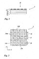
- Fig. 1 shows a multilayer body as a multilayer film body 1, which may be a hot stamping foil.
- a carrier film 10 which may be formed from an approximately 20 micron thick polyester film.
- the replication layer 12 may be a thermoplastic layer into which a pattern is formed by means of a replication tool. However, it can also be a UV-curing lacquer, in which the pattern is introduced by mask exposure by means of UV light or by taking an impression from a template with a surface structure.
- the replication layer 12 carries a partially perforated metallic layer 14, which may be made of aluminum, copper, silver, gold or chromium, for example.
- an adhesive layer 16 is applied on the side of the carrier film 10 facing away from the replication layer 12, with the aid of which the film body 1 can be transferred to a substrate.
- the adhesive layer 16 may preferably be a hot melt adhesive.
- the adhesive layer 16 may also be applied to the metal layer.
- the composite of replication layer, metal layer and adhesive layer can be designed as a transfer layer which is adhesively bonded to a substrate, wherein the carrier 10 can subsequently be removed.
- Fig. 2 now shows in detail the formation of the metallic layer 14 in plan view.
- the metallic layer 14 is subdivided into island-shaped regions 14m, which are respectively enclosed by demetallized regions 14d of the replication layer 12 with a width B.
- the demetallized areas 14d form a contiguous background area.
- the regions 14m are arranged in a grid with a screen width D, wherein the grid lines are designated position 14r.
- You are in the Fig. 2 illustrated embodiment formed as square fields with an edge length F, which is smaller than the grid width D: F D - B
- the metallized areas 14m may be formed as reflecting surfaces, so that the film body 1 appears as a mirror film.
- diffractive optical structures into the regions 14m, for example a hologram, or matt structures can be formed.
- a variety of optical effects can be generated that go beyond the replica of an optically uniform metallic surface.
- "metallic" microwaveable safety features, logos or labels can be placed on finished-meal packages that are not destroyed when heated in the microwave because they are electrically non-conductive metallic surfaces.
- Security elements such as those used on documents and bills, can be equipped in this way with an additional security feature, which consists in that such a security element is not destructible by microwave radiation.
- electronic devices such as television receivers can be provided with an electrically non-conductive metallic surface.
- the metal layer does not have to come to rest on the physical surface, but may also be embedded between dielectric layers, for example as part of a transfer layer or by injection molding in the manufacture of the housing components.
- the grid of in Fig. 2 illustrated embodiment is a square grid, whose grid width D in the coordinate directions x and y is the same, but can also be provided that the grid width D in the direction of the x-coordinate and the y-coordinate is different.
- the edge length F of the metallized region 14m and / or the width B of the demetallized region 14d may be formed differently.
- the metallized areas 14m may also be rectangular, circular, elliptical or otherwise shaped Areas with closed contour act. For a square grid, as in Fig. 2 As illustrated, squares, circles, and regular polygons may be preferred as the contour of the metallized regions.
- line-shaped metallized regions 14m which are separated from each other by line-shaped demetallized regions 14d.
- the metallized areas 14m are thus arranged in a line grid, i. in a one-dimensional grid.
- Such a film body is consequently made to be insulating in a direction perpendicular to the line-shaped regions 14m, 14d and to be conductive in a direction parallel to the line-shaped regions 14m, 14d.
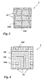
- Fig. 3 now shows a second embodiment in which the screen width in a random manner by ⁇ 40% by the value D 0 varies. It is in Fig. 3 around a film body 2 shown in plan view, in which both the metallized regions 14m and the demetallized regions 14d are formed irregularly shaped, wherein the deviations from a square grid are not larger than 40%. With such an embodiment, for example, the occurrence of moiré effects or disturbing diffraction effects can be avoided.
- Fig. 4 shows a schematic representation of a third embodiment, which by varying the first embodiment in Fig. 2 is formed.
- a metallic layer 34 is now structured such that, in addition to mutually insulated metallized regions 34m, regions of the metallic layer 34 are connected to one another and thus form conductor tracks 34l.
- antennas can be formed that are not visible to the unaided human eye.
- those under the metallized Regions 34m, 341 arranged replicating layer may have a diffraction-optical relief structure, for example in the form of a hologram, so also security elements can be provided with electrical functional elements.
- the film body of such a security element can have further layers which, for example, form an RFID tag, ie a circuit which serves for identification by means of radio waves.
- the background region that is to say between the metallized regions 34m, 34l, can be filled with an opaque colored layer.
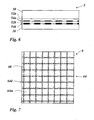
- Fig. 5 shows a fourth embodiment, in which a film 4 applied to a metallic layer 44 is formed as a substantially transparent electrically conductive layer.
- a film 4 applied to a metallic layer 44 is formed as a substantially transparent electrically conductive layer.
- island-shaped demetallized areas 44d are now surrounded by metallized strip-shaped areas 44m, which are connected to one another and thus form a coherent electrically conductive surface area.
- This surface area has the form of a close meshed network.
- the metallic layer 44 may be used, for example, as a shield against electromagnetic fields or for the discharge of static charges.
- the foil body 4 in the demetallized areas 44d may have a transparent colored layer in register with the strip-shaped metallic areas 44m. For better orientation are in Fig. 5 the grid lines 14r drawn (see. Fig. 2 ).
- Fig. 6 now shows a film body 5, which consists of a carrier layer 50, a first replication layer 52a, a first metallic layer 54a, a second replication layer 52b, a second metallic layer 54b and an adhesive layer 56.
- the two metallic layers 54a and 54b are arranged at such a distance from each other that the known interference effects can occur on thin layers.
- the two metallic layers 54a and 54b also have different thicknesses.
- the metallic layer 54a arranged closer to the carrier layer 50 is the thinner layer. It has a thickness in the lower nanometer range, so that it appears partially transparent in visible light. Because the transparency of a thin metal layer is inter alia dependent on the material, the required layer thickness is expediently determined by a series of experiments.
- Fig. 7 shows a film body 6 in plan view, in which the surface in the manner described above has island-shaped metallized areas 64m, which are surrounded by the metallized areas 64d.
- a micro-marking is introduced, which is formed in the illustrated embodiment as a micro-font, which is readable only with an optical aid, such as a strong magnifying glass or a microscope. But it can also be provided micrographics.
- the micro tag can reduce the electrical flashover strength of the demetallized regions 64d, provided that it has a metallized surface.
- the described embodiments include that the partial demetallization of the metallic layer occurs in the register.
- the metallic layer is arranged on the replication layer, which has a surface profile at least in regions. If now on the replication a metallic layer with uniform Surface density is applied based on the plane spanned by the replication layer, for example by vapor deposition in vacuum, the surface density or layer thickness can be chosen so that the applied metallic layer, depending on the local depth-to-width ratio of the surface profile a different has optical density. If the metallic layer is then used as an exposure mask for a photoresist, ie the photoresist is exposed through the metallic layer, then it can be developed into a register-accurate etching mask and the metallic layer can be partially demetallised in register.
- a surface profile with a high depth-to-width ratio for example with a depth-to-width ratio> 2
- the surface area profile can be formed into the regions of the replication layer arranged below the demetallized regions Replication layer under the metallized areas have a very low depth-to-width ratio .
- the dimensionless depth-to-width ratio is a characteristic feature of the surface enlargement, preferably of periodic structures.
- Such a structure forms “mountains” and “valleys” in a periodic sequence.
- Depth is here the distance between “mountain” and “valley”, as width the distance between two “mountains”.
- This effect can also be observed in the case of discretely distributed "valleys", which can be arranged at a distance that is many times greater than the depth of the "valleys".
- the depth of the "valley” is the width of the "valley” in order to properly describe the geometry of the "valley” by specifying the depth-to-width ratio.
- silver and gold As can be seen, have a high maximum reflectance R max and require one relatively small depth-to-width ratio for forming transparency.
- aluminum Al also has a high maximum reflectance R Max , it requires a higher depth-to-width ratio.
- it may be provided to form the metal layer of silver or gold. But it can also be provided to form the metal layer of other metals or of metal alloys.
- Table 2 now shows the calculation results obtained from rigorous diffraction calculations for surface structures formed as linear, sinusoidal grids with a grid spacing of 350 nm with different depth-to-width ratios.
- the degree of transparency, apart from the depth-to-width ratio depends on the polarization of the light radiated.
- the degree of transparency or the reflectance of the metal layer is wavelength-dependent. This effect is especially good for TE polarized light.
- the degree of transparency decreases when the angle of incidence of the light differs from the normal angle of incidence, i. the degree of transparency decreases when the light is not incident vertically.
- the metal layer in the region of the surface structure can be made transparent only in a limited incidence cone of the light. It can therefore be provided that the metal layer is formed opaque when viewed obliquely, this effect is useful for the use of the metal layer as a selective exposure mask.
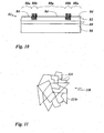
- the Fig. 8 to 10 Now show an embodiment for producing a passergenau teildemetallêten metallic layer.
- Fig. 8 shows a multilayer film body 81, which is like that in Fig. 1 described film body 1 is constructed.
- the film body 81 consists of several layers. In the exemplary embodiment shown, these are a carrier foil 80, a replication layer 82 and a metallic layer 84, as well as an adhesive layer 86, which is applied to the side of the carrier foil 80 facing away from the replication layer 82.
- a photosensitive layer 88 is applied on the metallic layer 84.
- the photosensitive layer 88 may be, for example, a UV-sensitive photoresist. This may be an organic layer which is applied in liquid form by conventional coating methods, such as gravure printing. It may also be provided that the photosensitive layer is vapor-deposited or laminated as a dry film.
- Fig. 11 shows the exposure of the photosensitive layer 88 from the side of the adhesive layer 86 with the photosensitive layer 88 being in the developed state.
- the exposure of the photosensitive layer 88 is provided with UV light 89, the metallic layer 84 acting as an exposure mask.
- the photosensitive layer 88 has areas 88u in which the layer 88 is obtained and areas 88b in which the layer 88 is removed as a result of development.
- the areas 88u are areas where the replication layer 82 is formed with a lower depth-to-width ratio-in the illustrated embodiment, it is zero-while in the areas 88b, the replication layer 88 has a surface texture has a high depth-to-width ratio.
- the metallic layer 84 is formed with a smaller thickness than in the areas 88u, so that the metallic layer 84 has a different transmission in both areas and thus the incident UV light is attenuated to varying degrees. It is not necessary to make the metallic layer so thin that the regions 88b appear transparent when viewed visually. A relatively low total transmission of the film body 81 can be compensated by an increased exposure dose of the photosensitive layer 88. It should also be noted that the exposure of the photosensitive Layer is typically provided in the near UV range, so that the visual viewing impression for the assessment of the transmission is not critical.
- the photosensitive layer 88 is formed of a positive photoresist.
- the exposed areas are soluble in the developer.
- the unexposed areas are soluble in the developer. It is possible in this way to demetall matters with a layout different areas of the metallic layer 84 register accurate. It may further be provided to further modify the metallic layer 84 with the aid of a subsequent galvanic treatment, for example to form it with increased layer thickness, for example conductor tracks as described above Fig. 4 shown to form with improved electrical conductivity.
- Fig. 10 now shows the film body 81 in its final state, after using an etchant, the metallic layer 84 is removed in the areas 88b.
- the metallic layer 84 is therefore only present in the regions 88u and thus forms electrically isolated islands from one another.
- Fig. 11 now shows a multi-layer body 110, which is divided into island areas 114 in a random manner.
- raster lines 114r are also randomly arranged and formed.
- the grid lines 114r are formed as a straight line. But they can also be curved lines. It can further be provided that the lines are formed with varying width.
- the grid width D and the width B are determined as mean values over all island areas 114.
- the size and shape of the island regions 114 may vary within a wide range, as well as the location of the centroids of the island regions. Nevertheless, it is envisaged that the island regions will typically have a mean size ⁇ 250 ⁇ m and the ratio between mean island size and width of the breaks will be between 5 and 200.
- the island regions 114 may be metallized and the background region characterized by the raster lines 114r may be demetallized or vice versa.
Landscapes
- Physics & Mathematics (AREA)
- General Physics & Mathematics (AREA)
- Engineering & Computer Science (AREA)
- Manufacturing & Machinery (AREA)
- Microelectronics & Electronic Packaging (AREA)
- Chemical & Material Sciences (AREA)
- General Chemical & Material Sciences (AREA)
- Chemical Kinetics & Catalysis (AREA)
- Computer Security & Cryptography (AREA)
- Laminated Bodies (AREA)
- Exposure Of Semiconductors, Excluding Electron Or Ion Beam Exposure (AREA)
- Credit Cards Or The Like (AREA)
- Diffracting Gratings Or Hologram Optical Elements (AREA)
Applications Claiming Priority (2)
| Application Number | Priority Date | Filing Date | Title |
|---|---|---|---|
| DE102005049891A DE102005049891A1 (de) | 2005-10-17 | 2005-10-17 | Metallisierter Mehrschichtkörper |
| PCT/EP2006/007860 WO2007045294A1 (de) | 2005-10-17 | 2006-08-09 | Mehrschichtkörper sowie verfahren zu dessen herstellung |
Publications (2)
| Publication Number | Publication Date |
|---|---|
| EP1937471A1 EP1937471A1 (de) | 2008-07-02 |
| EP1937471B1 true EP1937471B1 (de) | 2014-02-12 |
Family
ID=36953843
Family Applications (1)
| Application Number | Title | Priority Date | Filing Date |
|---|---|---|---|
| EP06776694.9A Active EP1937471B1 (de) | 2005-10-17 | 2006-08-09 | Mehrschichtkörper sowie verfahren zu dessen herstellung |
Country Status (12)
| Country | Link |
|---|---|
| US (1) | US8906491B2 (enExample) |
| EP (1) | EP1937471B1 (enExample) |
| JP (1) | JP5186378B2 (enExample) |
| KR (1) | KR101306403B1 (enExample) |
| CN (1) | CN101287594B (enExample) |
| AU (1) | AU2006303616B2 (enExample) |
| CA (1) | CA2621816C (enExample) |
| DE (1) | DE102005049891A1 (enExample) |
| ES (1) | ES2463422T3 (enExample) |
| RU (1) | RU2391214C2 (enExample) |
| TW (1) | TWI395675B (enExample) |
| WO (1) | WO2007045294A1 (enExample) |
Families Citing this family (27)
| Publication number | Priority date | Publication date | Assignee | Title |
|---|---|---|---|---|
| DE102005049891A1 (de) | 2005-10-17 | 2007-04-19 | Leonhard Kurz Gmbh & Co. Kg | Metallisierter Mehrschichtkörper |
| DE102007057658A1 (de) * | 2007-02-07 | 2009-06-04 | Leonhard Kurz Stiftung & Co. Kg | Sicherheitselement |
| DE102007027998A1 (de) * | 2007-06-14 | 2008-12-18 | Leonhard Kurz Gmbh & Co. Kg | Heißprägen von Leiterbahnen auf Photovoltaik-Silizium-Wafer |
| JP2009086385A (ja) * | 2007-09-29 | 2009-04-23 | Hoya Corp | フォトマスク及びフォトマスクの製造方法、並びにパターン転写方法 |
| DE102007051930A1 (de) * | 2007-10-29 | 2009-04-30 | Leonhard Kurz Gmbh & Co. Kg | Verfahren zur Herstellung einer Leiterbahnstruktur |
| JP5157394B2 (ja) * | 2007-11-29 | 2013-03-06 | 凸版印刷株式会社 | 光学機能付きrfid転写箔、光学機能付きrfidタグおよびそのタグを備えた情報記録媒体 |
| US7920297B2 (en) * | 2008-02-18 | 2011-04-05 | Vistaprint Technologies Limited | System and method for printing using variable-density white ink under-printed layer |
| DE102008013073B4 (de) | 2008-03-06 | 2011-02-03 | Leonhard Kurz Stiftung & Co. Kg | Verfahren zur Herstellung eines Folienelements und Folienelement |
| DE102008036481A1 (de) * | 2008-08-05 | 2010-02-11 | Giesecke & Devrient Gmbh | Verfahren zur Herstellung von Sicherheitselementen mit zueinander gepasserten Motiven |
| DE102008046511A1 (de) * | 2008-09-10 | 2010-03-11 | Giesecke & Devrient Gmbh | Darstellungsanordnung |
| US7995278B2 (en) * | 2008-10-23 | 2011-08-09 | 3M Innovative Properties Company | Methods of forming sheeting with composite images that float and sheeting with composite images that float |
| USD639445S1 (en) * | 2009-06-26 | 2011-06-07 | Labcon, North America | Container with label |
| DE202010001261U1 (de) * | 2010-01-22 | 2010-05-06 | Mondi Ag | Kunststofffolienbeutel mit Relief |
| KR101147420B1 (ko) * | 2010-02-24 | 2012-05-22 | 삼성모바일디스플레이주식회사 | 적층 시트 및 적층 시트 형성 방법 |
| DE102010056493A1 (de) | 2010-12-30 | 2012-07-05 | Polyic Gmbh & Co. Kg | Beheizbarer Spiegel |
| EP2579217A1 (de) * | 2011-10-04 | 2013-04-10 | Deutsche Post AG | Verfahren und Vorrichtung für die Markierung von Wertlabeln |
| DE102013101881A1 (de) * | 2013-02-26 | 2014-08-28 | Leonhard Kurz Stiftung & Co. Kg | Mehrschichtkörper und Verfahren zum Herstellen eines Mehrschichtkörpers |
| DE112015003824T5 (de) * | 2014-08-21 | 2017-05-04 | Sony Corporation | Gehäusekomponente, elektronische vorrichtung und gehäusekomponentenherstellungsverfahren |
| DE102014118366A1 (de) * | 2014-12-10 | 2016-06-16 | Ovd Kinegram Ag | Mehrschichtkörper und Verfahren zu dessen Herstellung |
| DE102015106800B4 (de) * | 2015-04-30 | 2021-12-30 | Leonhard Kurz Stiftung & Co. Kg | Verfahren zum Herstellen eines Mehrschichtkörpers |
| JP6603177B2 (ja) * | 2016-06-09 | 2019-11-06 | 株式会社ノリタケカンパニーリミテド | ハーフミラー型タッチスイッチパネル |
| DE102017003281A1 (de) * | 2017-04-04 | 2018-10-04 | Giesecke+Devrient Currency Technology Gmbh | Sicherheitselement mit Reliefstruktur und Herstellungsverfahren hierfür |
| JP6658800B2 (ja) * | 2018-06-12 | 2020-03-04 | コニカミノルタ株式会社 | 機能性細線パターン、透明導電膜付き基材、デバイス及び電子機器 |
| WO2020105013A1 (en) * | 2018-11-22 | 2020-05-28 | Sabic Global Technologies B.V. | Structural panels for electronic devices |
| CN113767716B (zh) | 2019-05-06 | 2024-07-30 | 3M创新有限公司 | 图案化导电制品 |
| CN110703577B (zh) * | 2019-11-21 | 2022-03-04 | 苏州大学 | 超表面彩色全息的制备方法及光学系统 |
| CN114280711B (zh) * | 2020-09-28 | 2023-07-11 | 比亚迪股份有限公司 | 透明板材及其制作方法、壳体和移动终端 |
Family Cites Families (20)
| Publication number | Priority date | Publication date | Assignee | Title |
|---|---|---|---|---|
| JPS593421B2 (ja) * | 1974-10-11 | 1984-01-24 | セントラル硝子株式会社 | ソウシヨクカガミノ セイゾウホウ |
| JPS5978987A (ja) * | 1982-10-29 | 1984-05-08 | マルイ工業株式会社 | 金属被膜上へのパタ−ン形成方法 |
| DE3430111C1 (de) * | 1984-08-16 | 1985-10-24 | Leonhard Kurz GmbH & Co, 8510 Fürth | Folie,insbesondere Heisspraegefolie,mit einer dekorativen Metallschicht und Verfahren zu deren Herstellung |
| JPS63158245A (ja) | 1986-12-22 | 1988-07-01 | 株式会社 麗光 | 成形用シ−ト |
| JPH0771880B2 (ja) | 1989-06-27 | 1995-08-02 | 株式会社麗光 | 転写材料の製造方法 |
| DE4132476A1 (de) | 1991-09-30 | 1993-04-01 | Matthiesen Geb Sievers Gerda | Verfahren, bedruckstoff und einrichtung zur verfielfaeltigung von holographischen feinstrukturen und anderen beugungsgittern auf printprodukte |
| RU2131615C1 (ru) * | 1993-02-10 | 1999-06-10 | Герда Маттизен | Способ одновременного изготовления реплик и прямой аппликации микроструктуры и устройство для его осуществления |
| DE4307487C2 (de) * | 1993-03-10 | 1995-08-24 | Horst Sitte Heispraegetechnik | Heißprägefolie und Verfahren zu deren Herstellung |
| US5800724A (en) * | 1996-02-14 | 1998-09-01 | Fort James Corporation | Patterned metal foil laminate and method for making same |
| JPH1044308A (ja) | 1996-07-30 | 1998-02-17 | Daiwa Seiko Inc | 装飾層を有する部材 |
| EP0816123B1 (en) | 1996-06-27 | 2009-02-18 | Daiwa Seiko Inc. | Member for fishing or sport tool |
| DE19813314A1 (de) * | 1998-03-26 | 1999-09-30 | Kurz Leonhard Fa | Prägefolie, insbesondere Heissprägefolie |
| JP2000117885A (ja) | 1998-10-16 | 2000-04-25 | Minnesota Mining & Mfg Co <3M> | 装飾フィルム及びその製造方法 |
| DE20002802U1 (de) * | 2000-02-16 | 2000-05-18 | Leonhard Kurz GmbH & Co, 90763 Fürth | Dekorfolie |
| TW583688B (en) * | 2002-02-21 | 2004-04-11 | Dainippon Printing Co Ltd | Electromagnetic shielding sheet and method of producing the same |
| AU2003222822A1 (en) * | 2002-05-14 | 2003-11-11 | Leonhard Kurz Gmbh And Co. Kg | Optically variable element comprising a sequence of thin-film layers |
| DE10256832A1 (de) * | 2002-12-04 | 2004-06-24 | Giesecke & Devrient Gmbh | Sicherheitsfolie und Verfahren zur Herstellung derselben |
| DE10328760B4 (de) * | 2003-06-25 | 2007-05-24 | Ovd Kinegram Ag | Optisches Sicherheitselement |
| DE10333704B4 (de) * | 2003-07-23 | 2009-12-17 | Ovd Kinegram Ag | Sicherheitselement zur RF-Identifikation |
| DE102005049891A1 (de) | 2005-10-17 | 2007-04-19 | Leonhard Kurz Gmbh & Co. Kg | Metallisierter Mehrschichtkörper |
-
2005
- 2005-10-17 DE DE102005049891A patent/DE102005049891A1/de not_active Withdrawn
-
2006
- 2006-08-09 ES ES06776694.9T patent/ES2463422T3/es active Active
- 2006-08-09 JP JP2008535903A patent/JP5186378B2/ja active Active
- 2006-08-09 CA CA2621816A patent/CA2621816C/en not_active Expired - Fee Related
- 2006-08-09 EP EP06776694.9A patent/EP1937471B1/de active Active
- 2006-08-09 TW TW095129158A patent/TWI395675B/zh active
- 2006-08-09 WO PCT/EP2006/007860 patent/WO2007045294A1/de not_active Ceased
- 2006-08-09 US US12/083,132 patent/US8906491B2/en active Active
- 2006-08-09 KR KR1020087009143A patent/KR101306403B1/ko active Active
- 2006-08-09 CN CN2006800384310A patent/CN101287594B/zh active Active
- 2006-08-09 AU AU2006303616A patent/AU2006303616B2/en not_active Ceased
- 2006-08-09 RU RU2008119511/02A patent/RU2391214C2/ru not_active IP Right Cessation
Also Published As
| Publication number | Publication date |
|---|---|
| CA2621816A1 (en) | 2007-04-26 |
| ES2463422T3 (es) | 2014-05-27 |
| US8906491B2 (en) | 2014-12-09 |
| JP5186378B2 (ja) | 2013-04-17 |
| DE102005049891A1 (de) | 2007-04-19 |
| CN101287594B (zh) | 2013-01-23 |
| CA2621816C (en) | 2014-03-18 |
| KR20080050616A (ko) | 2008-06-09 |
| CN101287594A (zh) | 2008-10-15 |
| AU2006303616A1 (en) | 2007-04-26 |
| AU2006303616B2 (en) | 2010-12-16 |
| KR101306403B1 (ko) | 2013-09-09 |
| TW200728107A (en) | 2007-08-01 |
| WO2007045294A1 (de) | 2007-04-26 |
| JP2009511308A (ja) | 2009-03-19 |
| TWI395675B (zh) | 2013-05-11 |
| US20090136721A1 (en) | 2009-05-28 |
| RU2391214C2 (ru) | 2010-06-10 |
| EP1937471A1 (de) | 2008-07-02 |
| RU2008119511A (ru) | 2009-11-27 |
Similar Documents
| Publication | Publication Date | Title |
|---|---|---|
| EP1937471B1 (de) | Mehrschichtkörper sowie verfahren zu dessen herstellung | |
| DE102005006231B4 (de) | Verfahren zur Herstellung eines Mehrschichtkörpers | |
| EP1786632B2 (de) | Metallisiertes sicherheitselement | |
| DE102005006277B4 (de) | Verfahren zur Herstellung eines Mehrschichtkörpers | |
| EP2117840B1 (de) | Sicherheitselement für ein sicherheitsdokument und verfahren zu seiner herstellung | |
| EP2991837B1 (de) | Optisch variables sicherheitselement | |
| DE69610632T2 (de) | Optisch variable sicherheitsvorrichtung mit metallischem muster | |
| EP1893416B1 (de) | Sicherheitsdokument | |
| EP2708371B1 (de) | Optisch variables Sicherheitselement mit zusätzlichem Auf-/Durchsichtseffekt | |
| EP2296909A2 (de) | Sicherheitselement mit gerasterter schicht auf einem lichtdurchlässigen substrat | |
| DE102012105571A1 (de) | Dekorelement, Sicherheitsdokument mit einem Dekorelement sowie Verfahren zur Herstellung eines Dekorelements | |
| WO2017097430A1 (de) | Sicherheitselement mit linsenrasterbild | |
| DE102008013073A1 (de) | Verfahren zur Herstellung eines Folienkörpers | |
| DE10216561A1 (de) | Sicherheitselement mit Makrostrukturen | |
| EP2981418B1 (de) | Sicherheitsfaden oder fensterelement für einen wertgegenstand und herstellverfahren dafür | |
| EP1599344B1 (de) | Sicherheitselement | |
| EP2821242B1 (de) | Sicherheitselement für Wertdokumente | |
| EP2086769B1 (de) | Sicherheitsfolie | |
| EP1547807B1 (de) | Sicherheitselement mit Beugungsstruktur und Verfahren zur Herstellung dieses Elements | |
| DE29700289U1 (de) | Flächenmuster |
Legal Events
| Date | Code | Title | Description |
|---|---|---|---|
| PUAI | Public reference made under article 153(3) epc to a published international application that has entered the european phase |
Free format text: ORIGINAL CODE: 0009012 |
|
| 17P | Request for examination filed |
Effective date: 20080218 |
|
| AK | Designated contracting states |
Kind code of ref document: A1 Designated state(s): AT BE BG CH CY CZ DE DK EE ES FI FR GB GR HU IE IS IT LI LT LU LV MC NL PL PT RO SE SI SK TR |
|
| DAX | Request for extension of the european patent (deleted) | ||
| GRAP | Despatch of communication of intention to grant a patent |
Free format text: ORIGINAL CODE: EPIDOSNIGR1 |
|
| INTG | Intention to grant announced |
Effective date: 20130829 |
|
| GRAP | Despatch of communication of intention to grant a patent |
Free format text: ORIGINAL CODE: EPIDOSNIGR1 |
|
| INTG | Intention to grant announced |
Effective date: 20131104 |
|
| GRAS | Grant fee paid |
Free format text: ORIGINAL CODE: EPIDOSNIGR3 |
|
| GRAA | (expected) grant |
Free format text: ORIGINAL CODE: 0009210 |
|
| AK | Designated contracting states |
Kind code of ref document: B1 Designated state(s): AT BE BG CH CY CZ DE DK EE ES FI FR GB GR HU IE IS IT LI LT LU LV MC NL PL PT RO SE SI SK TR |
|
| REG | Reference to a national code |
Ref country code: GB Ref legal event code: FG4D Free format text: NOT ENGLISH |
|
| REG | Reference to a national code |
Ref country code: CH Ref legal event code: EP |
|
| REG | Reference to a national code |
Ref country code: AT Ref legal event code: REF Ref document number: 651957 Country of ref document: AT Kind code of ref document: T Effective date: 20140215 |
|
| REG | Reference to a national code |
Ref country code: IE Ref legal event code: FG4D Free format text: LANGUAGE OF EP DOCUMENT: GERMAN |
|
| REG | Reference to a national code |
Ref country code: DE Ref legal event code: R096 Ref document number: 502006013531 Country of ref document: DE Effective date: 20140327 |
|
| REG | Reference to a national code |
Ref country code: CH Ref legal event code: NV Representative=s name: FIAMMENGHI-FIAMMENGHI, CH |
|
| REG | Reference to a national code |
Ref country code: SE Ref legal event code: TRGR |
|
| REG | Reference to a national code |
Ref country code: ES Ref legal event code: FG2A Ref document number: 2463422 Country of ref document: ES Kind code of ref document: T3 Effective date: 20140527 |
|
| REG | Reference to a national code |
Ref country code: NL Ref legal event code: VDEP Effective date: 20140212 |
|
| REG | Reference to a national code |
Ref country code: LT Ref legal event code: MG4D |
|
| PG25 | Lapsed in a contracting state [announced via postgrant information from national office to epo] |
Ref country code: LT Free format text: LAPSE BECAUSE OF FAILURE TO SUBMIT A TRANSLATION OF THE DESCRIPTION OR TO PAY THE FEE WITHIN THE PRESCRIBED TIME-LIMIT Effective date: 20140212 Ref country code: IS Free format text: LAPSE BECAUSE OF FAILURE TO SUBMIT A TRANSLATION OF THE DESCRIPTION OR TO PAY THE FEE WITHIN THE PRESCRIBED TIME-LIMIT Effective date: 20140612 |
|
| PG25 | Lapsed in a contracting state [announced via postgrant information from national office to epo] |
Ref country code: NL Free format text: LAPSE BECAUSE OF FAILURE TO SUBMIT A TRANSLATION OF THE DESCRIPTION OR TO PAY THE FEE WITHIN THE PRESCRIBED TIME-LIMIT Effective date: 20140212 Ref country code: PT Free format text: LAPSE BECAUSE OF FAILURE TO SUBMIT A TRANSLATION OF THE DESCRIPTION OR TO PAY THE FEE WITHIN THE PRESCRIBED TIME-LIMIT Effective date: 20140612 Ref country code: CY Free format text: LAPSE BECAUSE OF FAILURE TO SUBMIT A TRANSLATION OF THE DESCRIPTION OR TO PAY THE FEE WITHIN THE PRESCRIBED TIME-LIMIT Effective date: 20140212 |
|
| PG25 | Lapsed in a contracting state [announced via postgrant information from national office to epo] |
Ref country code: LV Free format text: LAPSE BECAUSE OF FAILURE TO SUBMIT A TRANSLATION OF THE DESCRIPTION OR TO PAY THE FEE WITHIN THE PRESCRIBED TIME-LIMIT Effective date: 20140212 |
|
| PG25 | Lapsed in a contracting state [announced via postgrant information from national office to epo] |
Ref country code: EE Free format text: LAPSE BECAUSE OF FAILURE TO SUBMIT A TRANSLATION OF THE DESCRIPTION OR TO PAY THE FEE WITHIN THE PRESCRIBED TIME-LIMIT Effective date: 20140212 Ref country code: RO Free format text: LAPSE BECAUSE OF FAILURE TO SUBMIT A TRANSLATION OF THE DESCRIPTION OR TO PAY THE FEE WITHIN THE PRESCRIBED TIME-LIMIT Effective date: 20140212 Ref country code: DK Free format text: LAPSE BECAUSE OF FAILURE TO SUBMIT A TRANSLATION OF THE DESCRIPTION OR TO PAY THE FEE WITHIN THE PRESCRIBED TIME-LIMIT Effective date: 20140212 |
|
| REG | Reference to a national code |
Ref country code: DE Ref legal event code: R097 Ref document number: 502006013531 Country of ref document: DE |
|
| PG25 | Lapsed in a contracting state [announced via postgrant information from national office to epo] |
Ref country code: SK Free format text: LAPSE BECAUSE OF FAILURE TO SUBMIT A TRANSLATION OF THE DESCRIPTION OR TO PAY THE FEE WITHIN THE PRESCRIBED TIME-LIMIT Effective date: 20140212 Ref country code: PL Free format text: LAPSE BECAUSE OF FAILURE TO SUBMIT A TRANSLATION OF THE DESCRIPTION OR TO PAY THE FEE WITHIN THE PRESCRIBED TIME-LIMIT Effective date: 20140212 |
|
| PLBE | No opposition filed within time limit |
Free format text: ORIGINAL CODE: 0009261 |
|
| STAA | Information on the status of an ep patent application or granted ep patent |
Free format text: STATUS: NO OPPOSITION FILED WITHIN TIME LIMIT |
|
| 26N | No opposition filed |
Effective date: 20141113 |
|
| REG | Reference to a national code |
Ref country code: DE Ref legal event code: R097 Ref document number: 502006013531 Country of ref document: DE Effective date: 20141113 |
|
| PG25 | Lapsed in a contracting state [announced via postgrant information from national office to epo] |
Ref country code: LU Free format text: LAPSE BECAUSE OF FAILURE TO SUBMIT A TRANSLATION OF THE DESCRIPTION OR TO PAY THE FEE WITHIN THE PRESCRIBED TIME-LIMIT Effective date: 20140809 Ref country code: MC Free format text: LAPSE BECAUSE OF FAILURE TO SUBMIT A TRANSLATION OF THE DESCRIPTION OR TO PAY THE FEE WITHIN THE PRESCRIBED TIME-LIMIT Effective date: 20140212 |
|
| PG25 | Lapsed in a contracting state [announced via postgrant information from national office to epo] |
Ref country code: BE Free format text: LAPSE BECAUSE OF NON-PAYMENT OF DUE FEES Effective date: 20140831 |
|
| REG | Reference to a national code |
Ref country code: IE Ref legal event code: MM4A |
|
| PG25 | Lapsed in a contracting state [announced via postgrant information from national office to epo] |
Ref country code: SI Free format text: LAPSE BECAUSE OF FAILURE TO SUBMIT A TRANSLATION OF THE DESCRIPTION OR TO PAY THE FEE WITHIN THE PRESCRIBED TIME-LIMIT Effective date: 20140212 |
|
| PG25 | Lapsed in a contracting state [announced via postgrant information from national office to epo] |
Ref country code: IE Free format text: LAPSE BECAUSE OF NON-PAYMENT OF DUE FEES Effective date: 20140809 |
|
| REG | Reference to a national code |
Ref country code: AT Ref legal event code: MM01 Ref document number: 651957 Country of ref document: AT Kind code of ref document: T Effective date: 20140809 |
|
| PG25 | Lapsed in a contracting state [announced via postgrant information from national office to epo] |
Ref country code: AT Free format text: LAPSE BECAUSE OF NON-PAYMENT OF DUE FEES Effective date: 20140809 |
|
| PG25 | Lapsed in a contracting state [announced via postgrant information from national office to epo] |
Ref country code: BG Free format text: LAPSE BECAUSE OF FAILURE TO SUBMIT A TRANSLATION OF THE DESCRIPTION OR TO PAY THE FEE WITHIN THE PRESCRIBED TIME-LIMIT Effective date: 20140212 |
|
| PG25 | Lapsed in a contracting state [announced via postgrant information from national office to epo] |
Ref country code: GR Free format text: LAPSE BECAUSE OF FAILURE TO SUBMIT A TRANSLATION OF THE DESCRIPTION OR TO PAY THE FEE WITHIN THE PRESCRIBED TIME-LIMIT Effective date: 20140513 |
|
| PG25 | Lapsed in a contracting state [announced via postgrant information from national office to epo] |
Ref country code: HU Free format text: LAPSE BECAUSE OF FAILURE TO SUBMIT A TRANSLATION OF THE DESCRIPTION OR TO PAY THE FEE WITHIN THE PRESCRIBED TIME-LIMIT; INVALID AB INITIO Effective date: 20060809 |
|
| REG | Reference to a national code |
Ref country code: FR Ref legal event code: PLFP Year of fee payment: 11 |
|
| REG | Reference to a national code |
Ref country code: FR Ref legal event code: PLFP Year of fee payment: 12 |
|
| REG | Reference to a national code |
Ref country code: FR Ref legal event code: PLFP Year of fee payment: 13 |
|
| PGFP | Annual fee paid to national office [announced via postgrant information from national office to epo] |
Ref country code: FI Payment date: 20190820 Year of fee payment: 14 Ref country code: IT Payment date: 20190821 Year of fee payment: 14 Ref country code: CZ Payment date: 20190730 Year of fee payment: 14 Ref country code: ES Payment date: 20190919 Year of fee payment: 14 Ref country code: SE Payment date: 20190826 Year of fee payment: 14 |
|
| PGFP | Annual fee paid to national office [announced via postgrant information from national office to epo] |
Ref country code: GB Payment date: 20190827 Year of fee payment: 14 |
|
| PGFP | Annual fee paid to national office [announced via postgrant information from national office to epo] |
Ref country code: CH Payment date: 20190826 Year of fee payment: 14 |
|
| REG | Reference to a national code |
Ref country code: FI Ref legal event code: MAE |
|
| REG | Reference to a national code |
Ref country code: SE Ref legal event code: EUG |
|
| REG | Reference to a national code |
Ref country code: CH Ref legal event code: PL |
|
| GBPC | Gb: european patent ceased through non-payment of renewal fee |
Effective date: 20200809 |
|
| PG25 | Lapsed in a contracting state [announced via postgrant information from national office to epo] |
Ref country code: CH Free format text: LAPSE BECAUSE OF NON-PAYMENT OF DUE FEES Effective date: 20200831 Ref country code: CZ Free format text: LAPSE BECAUSE OF NON-PAYMENT OF DUE FEES Effective date: 20200809 Ref country code: LI Free format text: LAPSE BECAUSE OF NON-PAYMENT OF DUE FEES Effective date: 20200831 Ref country code: FI Free format text: LAPSE BECAUSE OF NON-PAYMENT OF DUE FEES Effective date: 20200809 |
|
| PG25 | Lapsed in a contracting state [announced via postgrant information from national office to epo] |
Ref country code: SE Free format text: LAPSE BECAUSE OF NON-PAYMENT OF DUE FEES Effective date: 20200810 |
|
| PG25 | Lapsed in a contracting state [announced via postgrant information from national office to epo] |
Ref country code: IT Free format text: LAPSE BECAUSE OF NON-PAYMENT OF DUE FEES Effective date: 20200809 |
|
| PG25 | Lapsed in a contracting state [announced via postgrant information from national office to epo] |
Ref country code: GB Free format text: LAPSE BECAUSE OF NON-PAYMENT OF DUE FEES Effective date: 20200809 |
|
| REG | Reference to a national code |
Ref country code: ES Ref legal event code: FD2A Effective date: 20220110 |
|
| PG25 | Lapsed in a contracting state [announced via postgrant information from national office to epo] |
Ref country code: ES Free format text: LAPSE BECAUSE OF NON-PAYMENT OF DUE FEES Effective date: 20200810 |
|
| PGFP | Annual fee paid to national office [announced via postgrant information from national office to epo] |
Ref country code: DE Payment date: 20240715 Year of fee payment: 19 |
|
| PGFP | Annual fee paid to national office [announced via postgrant information from national office to epo] |
Ref country code: FR Payment date: 20240821 Year of fee payment: 19 |
|
| PGFP | Annual fee paid to national office [announced via postgrant information from national office to epo] |
Ref country code: TR Payment date: 20240730 Year of fee payment: 19 |