EP1937471B1 - Multi-layer body and method for producing the same - Google Patents
Multi-layer body and method for producing the same Download PDFInfo
- Publication number
- EP1937471B1 EP1937471B1 EP06776694.9A EP06776694A EP1937471B1 EP 1937471 B1 EP1937471 B1 EP 1937471B1 EP 06776694 A EP06776694 A EP 06776694A EP 1937471 B1 EP1937471 B1 EP 1937471B1
- Authority
- EP
- European Patent Office
- Prior art keywords
- layer
- surface structure
- region
- multilayer body
- metallic layer
- Prior art date
- Legal status (The legal status is an assumption and is not a legal conclusion. Google has not performed a legal analysis and makes no representation as to the accuracy of the status listed.)
- Active
Links
- 238000004519 manufacturing process Methods 0.000 title claims description 14
- 230000010076 replication Effects 0.000 claims description 53
- 238000000034 method Methods 0.000 claims description 22
- 229920002120 photoresistant polymer Polymers 0.000 claims description 22
- 230000003287 optical effect Effects 0.000 claims description 19
- 230000005540 biological transmission Effects 0.000 claims description 16
- 238000005406 washing Methods 0.000 claims description 15
- 238000005530 etching Methods 0.000 claims description 14
- 230000005855 radiation Effects 0.000 claims description 7
- 230000036961 partial effect Effects 0.000 claims description 6
- 238000012546 transfer Methods 0.000 claims description 6
- 239000000463 material Substances 0.000 claims description 4
- 239000002086 nanomaterial Substances 0.000 claims description 2
- 230000000873 masking effect Effects 0.000 claims 1
- 238000001429 visible spectrum Methods 0.000 claims 1
- 239000010410 layer Substances 0.000 description 238
- 239000010408 film Substances 0.000 description 35
- 229910052751 metal Inorganic materials 0.000 description 20
- 239000002184 metal Substances 0.000 description 20
- 230000000694 effects Effects 0.000 description 19
- 239000011888 foil Substances 0.000 description 8
- 229910052709 silver Inorganic materials 0.000 description 8
- 239000012790 adhesive layer Substances 0.000 description 7
- 239000010931 gold Substances 0.000 description 7
- BQCADISMDOOEFD-UHFFFAOYSA-N Silver Chemical compound [Ag] BQCADISMDOOEFD-UHFFFAOYSA-N 0.000 description 6
- 229910052782 aluminium Inorganic materials 0.000 description 6
- 229910052737 gold Inorganic materials 0.000 description 6
- 239000004332 silver Substances 0.000 description 6
- XAGFODPZIPBFFR-UHFFFAOYSA-N aluminium Chemical compound [Al] XAGFODPZIPBFFR-UHFFFAOYSA-N 0.000 description 5
- 230000001419 dependent effect Effects 0.000 description 5
- 238000013461 design Methods 0.000 description 5
- 238000001000 micrograph Methods 0.000 description 5
- 230000015572 biosynthetic process Effects 0.000 description 4
- 239000011651 chromium Substances 0.000 description 4
- 239000010949 copper Substances 0.000 description 4
- 230000005670 electromagnetic radiation Effects 0.000 description 4
- PCHJSUWPFVWCPO-UHFFFAOYSA-N gold Chemical compound [Au] PCHJSUWPFVWCPO-UHFFFAOYSA-N 0.000 description 4
- 150000002739 metals Chemical group 0.000 description 4
- 230000000737 periodic effect Effects 0.000 description 4
- 230000003068 static effect Effects 0.000 description 4
- RYGMFSIKBFXOCR-UHFFFAOYSA-N Copper Chemical compound [Cu] RYGMFSIKBFXOCR-UHFFFAOYSA-N 0.000 description 3
- 230000015556 catabolic process Effects 0.000 description 3
- 229910052804 chromium Inorganic materials 0.000 description 3
- 229910052802 copper Inorganic materials 0.000 description 3
- 238000011161 development Methods 0.000 description 3
- 238000004806 packaging method and process Methods 0.000 description 3
- 238000012216 screening Methods 0.000 description 3
- 230000000007 visual effect Effects 0.000 description 3
- VYZAMTAEIAYCRO-UHFFFAOYSA-N Chromium Chemical compound [Cr] VYZAMTAEIAYCRO-UHFFFAOYSA-N 0.000 description 2
- KDLHZDBZIXYQEI-UHFFFAOYSA-N Palladium Chemical compound [Pd] KDLHZDBZIXYQEI-UHFFFAOYSA-N 0.000 description 2
- 239000004020 conductor Substances 0.000 description 2
- 230000007423 decrease Effects 0.000 description 2
- 239000004922 lacquer Substances 0.000 description 2
- 229910001092 metal group alloy Inorganic materials 0.000 description 2
- 229910052760 oxygen Inorganic materials 0.000 description 2
- 239000001301 oxygen Substances 0.000 description 2
- 239000000758 substrate Substances 0.000 description 2
- 238000012795 verification Methods 0.000 description 2
- OKTJSMMVPCPJKN-UHFFFAOYSA-N Carbon Chemical compound [C] OKTJSMMVPCPJKN-UHFFFAOYSA-N 0.000 description 1
- MYMOFIZGZYHOMD-UHFFFAOYSA-N Dioxygen Chemical compound O=O MYMOFIZGZYHOMD-UHFFFAOYSA-N 0.000 description 1
- 240000005702 Galium aparine Species 0.000 description 1
- 239000004831 Hot glue Substances 0.000 description 1
- 238000003848 UV Light-Curing Methods 0.000 description 1
- 238000002679 ablation Methods 0.000 description 1
- 238000010521 absorption reaction Methods 0.000 description 1
- 230000002730 additional effect Effects 0.000 description 1
- 239000000853 adhesive Substances 0.000 description 1
- 230000001070 adhesive effect Effects 0.000 description 1
- 229910045601 alloy Inorganic materials 0.000 description 1
- 239000000956 alloy Substances 0.000 description 1
- 238000000149 argon plasma sintering Methods 0.000 description 1
- QVGXLLKOCUKJST-UHFFFAOYSA-N atomic oxygen Chemical compound [O] QVGXLLKOCUKJST-UHFFFAOYSA-N 0.000 description 1
- 230000002238 attenuated effect Effects 0.000 description 1
- 229910052799 carbon Inorganic materials 0.000 description 1
- 238000000576 coating method Methods 0.000 description 1
- 230000001427 coherent effect Effects 0.000 description 1
- 239000003086 colorant Substances 0.000 description 1
- 239000002131 composite material Substances 0.000 description 1
- 238000005034 decoration Methods 0.000 description 1
- 239000000975 dye Substances 0.000 description 1
- 230000005672 electromagnetic field Effects 0.000 description 1
- 238000011156 evaluation Methods 0.000 description 1
- 230000005284 excitation Effects 0.000 description 1
- 238000002474 experimental method Methods 0.000 description 1
- 239000011521 glass Substances 0.000 description 1
- 238000007646 gravure printing Methods 0.000 description 1
- 238000010438 heat treatment Methods 0.000 description 1
- 238000003384 imaging method Methods 0.000 description 1
- 238000001746 injection moulding Methods 0.000 description 1
- 239000012212 insulator Substances 0.000 description 1
- 239000002346 layers by function Substances 0.000 description 1
- 239000007788 liquid Substances 0.000 description 1
- 239000002932 luster Substances 0.000 description 1
- 239000011104 metalized film Substances 0.000 description 1
- 238000001465 metallisation Methods 0.000 description 1
- 230000003278 mimic effect Effects 0.000 description 1
- 239000012044 organic layer Substances 0.000 description 1
- 239000012785 packaging film Substances 0.000 description 1
- 229920006280 packaging film Polymers 0.000 description 1
- 229910052763 palladium Inorganic materials 0.000 description 1
- 238000000059 patterning Methods 0.000 description 1
- 239000002985 plastic film Substances 0.000 description 1
- 229920006255 plastic film Polymers 0.000 description 1
- 230000010287 polarization Effects 0.000 description 1
- 150000003071 polychlorinated biphenyls Chemical class 0.000 description 1
- 229920006267 polyester film Polymers 0.000 description 1
- 229920000642 polymer Polymers 0.000 description 1
- 238000007639 printing Methods 0.000 description 1
- 230000001681 protective effect Effects 0.000 description 1
- 230000002829 reductive effect Effects 0.000 description 1
- 238000002310 reflectometry Methods 0.000 description 1
- 230000003362 replicative effect Effects 0.000 description 1
- 239000004065 semiconductor Substances 0.000 description 1
- 238000001228 spectrum Methods 0.000 description 1
- 239000000126 substance Substances 0.000 description 1
- 230000001502 supplementing effect Effects 0.000 description 1
- 210000004243 sweat Anatomy 0.000 description 1
- 238000012360 testing method Methods 0.000 description 1
- 229920001169 thermoplastic Polymers 0.000 description 1
- 239000004416 thermosoftening plastic Substances 0.000 description 1
- 229910052719 titanium Inorganic materials 0.000 description 1
- 239000010936 titanium Substances 0.000 description 1
- 238000007740 vapor deposition Methods 0.000 description 1
- 230000004304 visual acuity Effects 0.000 description 1
- XLYOFNOQVPJJNP-UHFFFAOYSA-N water Substances O XLYOFNOQVPJJNP-UHFFFAOYSA-N 0.000 description 1
Images


Classifications
-
- B—PERFORMING OPERATIONS; TRANSPORTING
- B32—LAYERED PRODUCTS
- B32B—LAYERED PRODUCTS, i.e. PRODUCTS BUILT-UP OF STRATA OF FLAT OR NON-FLAT, e.g. CELLULAR OR HONEYCOMB, FORM
- B32B15/00—Layered products comprising a layer of metal
- B32B15/04—Layered products comprising a layer of metal comprising metal as the main or only constituent of a layer, which is next to another layer of the same or of a different material
- B32B15/08—Layered products comprising a layer of metal comprising metal as the main or only constituent of a layer, which is next to another layer of the same or of a different material of synthetic resin
-
- B—PERFORMING OPERATIONS; TRANSPORTING
- B42—BOOKBINDING; ALBUMS; FILES; SPECIAL PRINTED MATTER
- B42D—BOOKS; BOOK COVERS; LOOSE LEAVES; PRINTED MATTER CHARACTERISED BY IDENTIFICATION OR SECURITY FEATURES; PRINTED MATTER OF SPECIAL FORMAT OR STYLE NOT OTHERWISE PROVIDED FOR; DEVICES FOR USE THEREWITH AND NOT OTHERWISE PROVIDED FOR; MOVABLE-STRIP WRITING OR READING APPARATUS
- B42D25/00—Information-bearing cards or sheet-like structures characterised by identification or security features; Manufacture thereof
- B42D25/30—Identification or security features, e.g. for preventing forgery
- B42D25/36—Identification or security features, e.g. for preventing forgery comprising special materials
- B42D25/373—Metallic materials
-
- B—PERFORMING OPERATIONS; TRANSPORTING
- B42—BOOKBINDING; ALBUMS; FILES; SPECIAL PRINTED MATTER
- B42D—BOOKS; BOOK COVERS; LOOSE LEAVES; PRINTED MATTER CHARACTERISED BY IDENTIFICATION OR SECURITY FEATURES; PRINTED MATTER OF SPECIAL FORMAT OR STYLE NOT OTHERWISE PROVIDED FOR; DEVICES FOR USE THEREWITH AND NOT OTHERWISE PROVIDED FOR; MOVABLE-STRIP WRITING OR READING APPARATUS
- B42D25/00—Information-bearing cards or sheet-like structures characterised by identification or security features; Manufacture thereof
- B42D25/30—Identification or security features, e.g. for preventing forgery
- B42D25/324—Reliefs
-
- B—PERFORMING OPERATIONS; TRANSPORTING
- B42—BOOKBINDING; ALBUMS; FILES; SPECIAL PRINTED MATTER
- B42D—BOOKS; BOOK COVERS; LOOSE LEAVES; PRINTED MATTER CHARACTERISED BY IDENTIFICATION OR SECURITY FEATURES; PRINTED MATTER OF SPECIAL FORMAT OR STYLE NOT OTHERWISE PROVIDED FOR; DEVICES FOR USE THEREWITH AND NOT OTHERWISE PROVIDED FOR; MOVABLE-STRIP WRITING OR READING APPARATUS
- B42D25/00—Information-bearing cards or sheet-like structures characterised by identification or security features; Manufacture thereof
- B42D25/30—Identification or security features, e.g. for preventing forgery
- B42D25/328—Diffraction gratings; Holograms
-
- B—PERFORMING OPERATIONS; TRANSPORTING
- B42—BOOKBINDING; ALBUMS; FILES; SPECIAL PRINTED MATTER
- B42D—BOOKS; BOOK COVERS; LOOSE LEAVES; PRINTED MATTER CHARACTERISED BY IDENTIFICATION OR SECURITY FEATURES; PRINTED MATTER OF SPECIAL FORMAT OR STYLE NOT OTHERWISE PROVIDED FOR; DEVICES FOR USE THEREWITH AND NOT OTHERWISE PROVIDED FOR; MOVABLE-STRIP WRITING OR READING APPARATUS
- B42D25/00—Information-bearing cards or sheet-like structures characterised by identification or security features; Manufacture thereof
- B42D25/40—Manufacture
- B42D25/405—Marking
- B42D25/415—Marking using chemicals
- B42D25/42—Marking using chemicals by photographic processes
-
- B—PERFORMING OPERATIONS; TRANSPORTING
- B42—BOOKBINDING; ALBUMS; FILES; SPECIAL PRINTED MATTER
- B42D—BOOKS; BOOK COVERS; LOOSE LEAVES; PRINTED MATTER CHARACTERISED BY IDENTIFICATION OR SECURITY FEATURES; PRINTED MATTER OF SPECIAL FORMAT OR STYLE NOT OTHERWISE PROVIDED FOR; DEVICES FOR USE THEREWITH AND NOT OTHERWISE PROVIDED FOR; MOVABLE-STRIP WRITING OR READING APPARATUS
- B42D25/00—Information-bearing cards or sheet-like structures characterised by identification or security features; Manufacture thereof
- B42D25/40—Manufacture
- B42D25/45—Associating two or more layers
-
- B—PERFORMING OPERATIONS; TRANSPORTING
- B44—DECORATIVE ARTS
- B44C—PRODUCING DECORATIVE EFFECTS; MOSAICS; TARSIA WORK; PAPERHANGING
- B44C1/00—Processes, not specifically provided for elsewhere, for producing decorative surface effects
- B44C1/16—Processes, not specifically provided for elsewhere, for producing decorative surface effects for applying transfer pictures or the like
- B44C1/165—Processes, not specifically provided for elsewhere, for producing decorative surface effects for applying transfer pictures or the like for decalcomanias; sheet material therefor
- B44C1/17—Dry transfer
- B44C1/1712—Decalcomanias applied under heat and pressure, e.g. provided with a heat activable adhesive
- B44C1/1716—Decalcomanias provided with a particular decorative layer, e.g. specially adapted to allow the formation of a metallic or dyestuff layer on a substrate unsuitable for direct deposition
-
- G—PHYSICS
- G03—PHOTOGRAPHY; CINEMATOGRAPHY; ANALOGOUS TECHNIQUES USING WAVES OTHER THAN OPTICAL WAVES; ELECTROGRAPHY; HOLOGRAPHY
- G03H—HOLOGRAPHIC PROCESSES OR APPARATUS
- G03H1/00—Holographic processes or apparatus using light, infrared or ultraviolet waves for obtaining holograms or for obtaining an image from them; Details peculiar thereto
- G03H1/0005—Adaptation of holography to specific applications
- G03H1/0011—Adaptation of holography to specific applications for security or authentication
-
- G—PHYSICS
- G03—PHOTOGRAPHY; CINEMATOGRAPHY; ANALOGOUS TECHNIQUES USING WAVES OTHER THAN OPTICAL WAVES; ELECTROGRAPHY; HOLOGRAPHY
- G03H—HOLOGRAPHIC PROCESSES OR APPARATUS
- G03H1/00—Holographic processes or apparatus using light, infrared or ultraviolet waves for obtaining holograms or for obtaining an image from them; Details peculiar thereto
- G03H1/02—Details of features involved during the holographic process; Replication of holograms without interference recording
- G03H1/0236—Form or shape of the hologram when not registered to the substrate, e.g. trimming the hologram to alphanumerical shape
-
- G—PHYSICS
- G03—PHOTOGRAPHY; CINEMATOGRAPHY; ANALOGOUS TECHNIQUES USING WAVES OTHER THAN OPTICAL WAVES; ELECTROGRAPHY; HOLOGRAPHY
- G03H—HOLOGRAPHIC PROCESSES OR APPARATUS
- G03H1/00—Holographic processes or apparatus using light, infrared or ultraviolet waves for obtaining holograms or for obtaining an image from them; Details peculiar thereto
- G03H1/02—Details of features involved during the holographic process; Replication of holograms without interference recording
- G03H1/0252—Laminate comprising a hologram layer
-
- H—ELECTRICITY
- H05—ELECTRIC TECHNIQUES NOT OTHERWISE PROVIDED FOR
- H05K—PRINTED CIRCUITS; CASINGS OR CONSTRUCTIONAL DETAILS OF ELECTRIC APPARATUS; MANUFACTURE OF ASSEMBLAGES OF ELECTRICAL COMPONENTS
- H05K5/00—Casings, cabinets or drawers for electric apparatus
- H05K5/02—Details
- H05K5/0217—Mechanical details of casings
- H05K5/0243—Mechanical details of casings for decorative purposes
-
- B42D2033/10—
-
- G—PHYSICS
- G03—PHOTOGRAPHY; CINEMATOGRAPHY; ANALOGOUS TECHNIQUES USING WAVES OTHER THAN OPTICAL WAVES; ELECTROGRAPHY; HOLOGRAPHY
- G03H—HOLOGRAPHIC PROCESSES OR APPARATUS
- G03H1/00—Holographic processes or apparatus using light, infrared or ultraviolet waves for obtaining holograms or for obtaining an image from them; Details peculiar thereto
- G03H1/02—Details of features involved during the holographic process; Replication of holograms without interference recording
- G03H1/024—Hologram nature or properties
- G03H1/0244—Surface relief holograms
-
- G—PHYSICS
- G03—PHOTOGRAPHY; CINEMATOGRAPHY; ANALOGOUS TECHNIQUES USING WAVES OTHER THAN OPTICAL WAVES; ELECTROGRAPHY; HOLOGRAPHY
- G03H—HOLOGRAPHIC PROCESSES OR APPARATUS
- G03H1/00—Holographic processes or apparatus using light, infrared or ultraviolet waves for obtaining holograms or for obtaining an image from them; Details peculiar thereto
- G03H1/04—Processes or apparatus for producing holograms
- G03H1/18—Particular processing of hologram record carriers, e.g. for obtaining blazed holograms
- G03H2001/187—Trimming process, i.e. macroscopically patterning the hologram
- G03H2001/188—Demetallisation, i.e. removing the enhancing metallic layer
-
- G—PHYSICS
- G03—PHOTOGRAPHY; CINEMATOGRAPHY; ANALOGOUS TECHNIQUES USING WAVES OTHER THAN OPTICAL WAVES; ELECTROGRAPHY; HOLOGRAPHY
- G03H—HOLOGRAPHIC PROCESSES OR APPARATUS
- G03H2250/00—Laminate comprising a hologram layer
- G03H2250/10—Laminate comprising a hologram layer arranged to be transferred onto a carrier body
-
- Y—GENERAL TAGGING OF NEW TECHNOLOGICAL DEVELOPMENTS; GENERAL TAGGING OF CROSS-SECTIONAL TECHNOLOGIES SPANNING OVER SEVERAL SECTIONS OF THE IPC; TECHNICAL SUBJECTS COVERED BY FORMER USPC CROSS-REFERENCE ART COLLECTIONS [XRACs] AND DIGESTS
- Y10—TECHNICAL SUBJECTS COVERED BY FORMER USPC
- Y10T—TECHNICAL SUBJECTS COVERED BY FORMER US CLASSIFICATION
- Y10T428/00—Stock material or miscellaneous articles
- Y10T428/24—Structurally defined web or sheet [e.g., overall dimension, etc.]
- Y10T428/24802—Discontinuous or differential coating, impregnation or bond [e.g., artwork, printing, retouched photograph, etc.]
Definitions
- the invention relates to a multilayer body having a replication layer which has microscopically fine pattern areas, and to a method for producing a multilayer body having adjustable or defined electrical conductivity.
- metallized multilayer bodies in particular metallized films, which have a reflective or matt or otherwise structured surface which is electrically conductive.
- the electrically conductive surface may be troublesome, for example when the foils are intended to decorate enclosures of electronic equipment, or when the foils are to serve as packaging for food exposed to the electromagnetic radiation of a microwave oven.
- Such packaging can also contain security features with a metallic surface, which can also be thermally destroyed by microwave radiation.
- the invention is based on the object of specifying a multi-layer body with adjustable or defined electrical conductivity and a manufacturing method that is cost-effective and suitable for mass production.
- the object of the invention is achieved with a method for producing a multilayer body with adjustable or defined electrical conductivity, wherein it is provided that in a first region of a replication layer of the multilayer body, a diffractive first surface structure is formed, that a metallic layer on the replication in the first region and in a second region in which the first surface structure is not formed in the replication layer, wherein either the first region or the second region is formed by a plurality of microscopically fine pattern areas, in a line grid or in a surface grid with the Rastenrveite D are arranged and which are each separated by the, each of the sub-areas completely delimiting or enclosing the second area or first area separated from each other at a distance B from each other that on the metallic layer a photoemp is applied sensitive layer or as a replication layer, a photosensitive wash mask is applied, that the photosensitive layer or wash mask is exposed through the metallic layer, so that the photosensitive layer or washing mask is exposed differently by the first surface structure in the first and in the second region and that
- the object is further achieved with a multi-layer body, in particular a transfer film, with a replication layer and a metallic layer arranged on the replication layer, wherein it is provided that the multi-layer body has a multiplicity of microscopically fine pattern areas and a background area completely delimiting or enclosing the pattern areas the pattern areas are arranged in a line grid or in an area grid with the screen width D, the pattern areas are separated from each other by the background area at a distance B from one another, the screen pitch D is smaller than 500 ⁇ m, and the ratio of the grid spacing D to the distance B in FIG Range of 5 to 200, and that the metallic layer is removed either in the background area or in the pattern areas.
- the multi-layer body has a multiplicity of microscopically fine pattern areas and a background area completely delimiting or enclosing the pattern areas the pattern areas are arranged in a line grid or in an area grid with the screen width D, the pattern areas are separated from each other by the background area at a distance B from one another, the screen pitch
- the metallic layer applied to the surface structure itself forms an optical exposure mask, the optical effect of the metallic layer being determined by the surface structure on which it is arranged.
- in-register partial removal of the metallic layer itself acting as an exposure mask can be achieved, in the high resolution and quality required to fabricate the microscopically fine island structures.
- grid is not only used here as a uniform subdivision of a surface. Rather, uneven or random grids, such as frequency-modulated grids, as used in the printing industry, understood by "raster". Thus, it is expressly included subdivisions of the area in island areas, which are formed completely stochastic.
- the lines between the island areas can also be curved and / or be of varying thickness.
- the grid width D and / or the distance B can also be average values of the totality.
- they can be line grids, ie one-dimensional grids or multi-dimensional grids, for example area grids.
- the invention thus provides a production method for partially metallized multilayer bodies, in particular partially metallized foils with microscopically fine island structures, which is particularly effective and inexpensive.
- the metallic layer of a multilayer body according to the invention which is provided with the above-specified arrangement of metallized island-shaped pattern areas, appears to the unarmed human eye as a homogeneous metallic surface.
- the metallic layer is electrically non-conductive, but throughout for electromagnetic radiation up to the microwave range.
- the multilayer body can therefore be exposed to, for example, the radiation of a microwave without noticeably heating.
- a metallically appearing, but electrically non-conductive surface can be realized.
- the effect of the electrical conductivity can be made frequency-dependent. This means that depending on the excitation frequency, an electrical conductivity may or may not be present.
- a multilayer body formed as a film is perceived as a metallic mirror film.
- Such a film can be used, for example, for the decoration of electrical appliances, such as television receivers, which are to have an electrically non-conductive surface.
- a transparent film having an electrically conductive surface can be produced.
- Such an electrically conductive film may have, for example, demetallized pattern areas which are surrounded by a metallized background area.
- This film can be used, for example, as a transparent shielding film, which despite its transparency because of the reticulated metallized background region to shield electromagnetic radiation or is able to dissipate static electrical charges.
- Any electrical conductivities can be adjusted, for example, by varying the layer thickness of the metallic layer or by varying the ratio D / B.
- a multilayer body may be formed as a film which is insulating in one direction and conducting in another direction.
- the screen width D is selected in the range of 1 .mu.m to 500 .mu.m, preferably in the range of 5 .mu.m to 300 .mu.m. It can also be provided that the grid width in the range from 10 ⁇ m to 250 ⁇ m. If the screen width D is in these ranges, conspicuous diffraction effects of the multilayer body are avoided on the one hand, and on the other hand the pattern areas are not visible in detail since the subdivision lies below the resolution limit of the unarmed human eye.
- the ratio of the grid width D to the distance B in the range of 5 to 200 is selected.
- the ratio D / B in particular the electrical breakdown strength of the multilayer body can be influenced.
- the metallic layer is applied to a plane spanned by the replication layer over its entire surface in a constant areal density, preferably vapor-deposited.
- Such a method is inexpensive and well controllable in the layer thickness of the metallic layer.
- the metallic layer is applied to the replication completely over the entire surface in a thickness at which the metallic layer has an optical density of between 1 and 7 in a region of the replication layer without a surface structure.
- the effect of the different transmission, in particular transparency, is set by the depth-to-width ratio of the surface structure of the replication layer described in more detail below.
- the metallic layer may be a metal, for example aluminum, silver, gold, copper, chromium or palladium, or an alloy of these and / or other metals, or a layer sequence of the metals listed above.
- the transmission in particular the transparency of the metallic layer in the first region relative to the transmission, in particular, increases the transparency of the metallic layer in the second region, or vice versa.
- the transmission, in particular the transparency, or the optical density of the metallic layer can thus be influenced by means of the surface structure in the replication layer. Even slight differences in transmission or transparency, which are no longer perceptible, for example, by the human eye, may be sufficient under suitable production conditions to use the metallic layer as an exposure mask. Because the replication layer can be inexpensively formed with a very fine surface structure, the required high resolutions in the partial demetallization of the metallic layer can also be carried out inexpensively.
- the first surface structure has a greater relief depth than the second surface structure or vice versa.
- the product of Spatialfrequenz and relief depth of the first surface structure is greater than the product of Spatialfrequenz and relief depth of the second surface structure or vice versa.
- the spatial frequency is given in lines / mm and is a characteristic feature of diffractive structures. In the preferred screen width of 5 microns to 300 microns, it is advantageously chosen between 500 lines / mm and 5000 lines / mm. In structures with stochastic profile, such as matte structures, is a typical characteristic Distance between surveys used or, for example, the so-called correlation length. This parameter is analogously between 0.2 and 2.0 microns.
- a surface structure having a high depth-to-width ratio of the individual structural elements, in particular with a depth-to-width ratio> 0.3 is molded and that the second surface structure is formed as a surface structure with a lower depth-to-width ratio, or vice versa.
- the dimensionless depth-to-width ratio is a characteristic feature of surface enlargement by preferably periodic structures.
- Such a structure forms “mountains” and “valleys” in a periodic sequence.
- Depth is here the distance between “mountain” and “valley”, as width the distance between two “mountains”.
- This effect can also be observed in the case of discretely distributed "valleys", which can be arranged at a distance that is many times greater than the depth of the "valleys".
- the depth of the "valley” should be related to the width of the "valley” to properly describe the geometry of the "valley” by specifying the depth-to-width ratio.
- a photosensitive material having a binary characteristic is applied as the photosensitive layer or as a photosensitive wash mask and that the photosensitive layer or the photosensitive wash mask is exposed through the metallic layer in an exposure intensity and exposure time such that the photosensitive layer or photosensitive layer is exposed the photosensitive washing mask in the first region or in the second region, in which the transmission, in particular the transparency of the metallic layer is conditionally increased by the first surface structure, is activated and is not activated in the second region, or vice versa.
- UV radiation is more energetic than daylight and therefore often preferred.
- the areas of the photosensitive washing mask activated by the exposure and the areas of the metallic layer arranged thereon can be removed in a washing process.
- the exposed photosensitive layer is developed and that the developed photosensitive layer forms an etching mask for the metallic layer.
- a further advantageous embodiment provides that the photosensitive layer is activated by the exposure in the first region in which the transmission, in particular the transparency of the metallic layer is increased by the first surface structure, and that the activated photoactivatable layer is an etchant for the metallic Layer forms.
- the photosensitive layer is formed of a photoresist.
- the photoresist may be formed as a positive photoresist or as a negative photoresist.
- the photosensitive layer may also be a photopolymer.
- the exposure takes place in each case on the photoresist side, but it can also take place through the metallic layer.
- the structuring can also be done by direct laser irradiation (ablation), without the detour using photoresist as "amplifier".
- absorption irradiation
- photoresist as "amplifier”.
- the structuring can take place by utilizing the structure-dependent etching behavior of the metallic layer. Namely, if patterned surfaces are vapor-deposited with a metallic layer and exposed to a suitable etching medium, high aspect ratio regions appear transparent after a certain time, while unstructured regions or low aspect ratio regions still appear largely opaque. Such a time-controlled etching process ends, for example, when in regions of the replication layer with surface relief structure and effectively thinner layer thickness of the metallic layer transparency was generated, while in regions of the replication without surface structure and effectively thicker layer thickness of the metallic layer still opaque metallic layer is present.
- the etching of the metallic layer which also occurs in the unstructured regions is usually precompensated by an initially increased optical density of the vapor-deposited metallic layer.
- the formation of a mobile phone housing may be provided.
- the combination may be provided with classical demetallization. It can therefore be provided that further areas are demetallized completely or partially by classical demetallization.
- one or more layers of the multilayer body can be colored to produce a visual impression.
- the multilayer body may furthermore comprise at least one transparent or opaque colored layer formed over the whole area or partially. It is particularly preferred if the at least one colored layer is formed in register with the metallic layer, in particular in the first or second region free of the metallic layer. As a result, a colored impression can be achieved and / or the multilayer body can be made opaque despite the partial metallization.
- the at least one colored layer is arranged in the first or second region free of the metallic layer and furthermore has a color similar to the metallic layer. For example, in the case of a silver metallic layer, a gray or, in the case of a golden metallic layer, a yellowish layer is preferred which helps to suggest to the human eye a reflective metallic layer without interruptions.
- the at least one colored layer is formed either as an electrically conductive layer, which contains, for example, non-metallic electrically conductive substances, such as carbon or polymers, or as an electrically insulating layer, which, for example, increases the breakdown voltage .
- the at least one colored layer can also be a semiconducting layer.
- the at least one colored layer contains no metal.
- CMYK complementary metal-oxide-semiconductor
- dyes which are opaque or transparent only in a certain wavelength range and which act as filters, for example when exposed to UV light. This can be achieved by pressure additional local structuring of the conductivity, which can also be influenced by the choice of the spectrum of the light source.
- the metallic layer is galvanically reinforced. It is also possible to reinforce the layer by a second metal or a metal alloy. After exposure, the photoresist is partially removed so that corresponding metallic areas of the metallic layer are exposed. The galvanic structure now takes place in the exposed areas, while the photoresist-covered areas essentially serve to ensure the necessary electrical conductivity for the galvanic structure. Subsequently, the photoresist is also removed from these areas. The remaining thin metallic layer in the background area becomes then removed by etching.
- the grid is formed with a constant screen width D.
- the grid is formed with a non-constant grid width D.
- the screen width D preferably varies randomly over a range of ⁇ 40%. With such a randomized variation of the screen ruling, the occurrence of moire can be counteracted, and diffraction effects can be avoided, which may occur in the case of screens having a constant screen ruling. can make disturbing noticeable.
- the first or second surface structure may be formed as an optically active, reflective or transmitting light-diffractive and / or refractive and / or light-scattering microstructure or nanostructure, for example as a lattice structure, such as a linear lattice or a lattice, as a superposition of a plurality of lattice structures, as an isotropic or anisotropic matt structure, as binary or continuous Fresnel lens, as a microprism, as Blazegitter, as a combination structure or as a macrostructure.
- a lattice structure such as a linear lattice or a lattice, as a superposition of a plurality of lattice structures, as an isotropic or anisotropic matt structure, as binary or continuous Fresnel lens, as a microprism, as Blazegitter, as a combination structure or as a macrostructure.
- a lattice structure such as a linear lattice
- the reflectivity is only slightly reduced by the partial demetallization, so that the hologram is perceived at substantially the same intensity as an electrically conductive version. Because the Rasttation is below the resolution limit of the unaided eye, it remains hidden from the human observer, if the screening is chosen such that no moiré effects occur with design elements of the hologram. Even with machine evaluation no quality losses are to be feared.
- the transmission behavior of the non-conductive mirror foil can be changed clearly recognizable, while the reflection behavior varies only imperceptibly. When viewed in reflected light, therefore, no information is visible, while it opens up when viewed in transmitted light, for example, as a pictorial representation.
- the multilayer body has a second metallic layer, which is arranged in register with a first metallic layer and / or the at least one colored layer.
- the metallic layers may have different thicknesses, as a result of which, on the one hand, the electrical properties of the multi-layer body and, on the other hand, the optical properties of the multi-layer body can be designed further.
- At least one of the metallic layers is applied in a layer thickness in which it is partially transparent in the visible range.
- the layer thickness to be selected depends on the material. Layer thicknesses of a few 10 nm can already appear opaque, ie non-transparent. For example, aluminum appears opaque when its optical density is in the range of 1 to 5. It is further determined by the depth-to-width ratio of the surface structure of the replication layer on which the metallic layer is deposited.
- the metallic layer may still have an electrical conductivity which is sufficient for many applications. It can be provided, for example, to use such a film designed as a multilayer body for shielding electromagnetic radiation or for dissipating static electrical charges.
- the multilayer body can thus u.a. be used as a packaging film for static-sensitive components such as microprocessors. It can also be provided that such a film is formed only with a metallic layer, as described above.
- the distance between the metallic layers is chosen such that interference effects occur.
- the metallic layers can be arranged in (2n + 1) . ⁇ / 2 or (4n + 1) .lambda. / 4-distance, where n is an integer incl. 0 and .lambda. Denotes the wavelength of the light.
- the interference on thin layers produces color changes, as are known, for example, from oil films on water surfaces. In this way, interesting optical effects can be formed which can serve, for example, decorative purposes or can form a security feature that is difficult to imitate.
- the metallic layers have a different first surface structure and / or second surface structure and / or that their first regions and / or their second regions are arranged differently.
- the pattern areas of the two metallic Layers can for example be arranged in a checkerboard manner offset from each other and be executed with different color metals, such as aluminum and copper.
- the pattern areas of a layer can also form groups that can be perceived by the human eye due to their dimensions. The groups could, for example, be pixels that are arranged overall in a pictorial or textual representation.
- the first surface structure and / or the second surface structure is a diffractive surface structure, for example a hologram, Kinegram ® or the like.
- a diffractive surface structure for example a hologram, Kinegram ® or the like.
- a metallized hologram or Kinegram ® be provided with an electrically non-conductive surface or reflection layer. It can therefore be applied as a safety feature on food packaging, which should be exposed together with the contents in a microwave of microwave radiation. But it is also possible to attach such security features on bills or documents and make the authenticity check by microwave irradiation. In this way, counterfeit security features can be identified and destroyed at the same time.
- first surface structure and / or the second surface structure is a matt structure. It is shown above that it is possible with the method according to the invention to produce mirror films which have an electrically non-conductive surface.
- the surface structure of the island-like metallized regions may also be formed as a matte structure or otherwise designed to mimic the multiple optical appearance of metallic surfaces, such as matte brushed surfaces Metallic luster.
- the metallic reflection layer can also be covered with further transparent or colored layers.
- the pattern area and / or the background area can be substructured in the form of a microtext or a micrograph.
- the microtext or micrograph can be a safety feature that is imperceptible to the unaided human eye and is difficult to imitate.
- the microtext or the micrograph or a barcode may be formed as metallized or non-metallized subregions.
- non-metallized subregions can be formed in a metallized pattern region, in that a different surface structure is formed in the replication layer than in the pattern region itself.
- the envelope of the other surface structure forms the edge contour of the microtext or the micrograph.
- it can also be a metallized subregion, which differs in its optical effect from the pattern region surrounding it, that is to say, for example, due to color change when tilting or tilting the film.
- microtext or micrographics may be incorporated in the background region, it being advantageously possible to provide that metallized microtext or micrograph is separated from the metallized pattern regions by non-metallized regions if the film is to be formed with a non-conductive surface.
- the pattern areas and / or the background area are substructured in the form of a hidden pattern that can be opened by a moiré verifier, that is to say a separate verification sign is. Even such a security feature is difficult to imitate.
- Fig. 1 shows a multilayer body as a multilayer film body 1, which may be a hot stamping foil.
- a carrier film 10 which may be formed from an approximately 20 micron thick polyester film.
- the replication layer 12 may be a thermoplastic layer into which a pattern is formed by means of a replication tool. However, it can also be a UV-curing lacquer, in which the pattern is introduced by mask exposure by means of UV light or by taking an impression from a template with a surface structure.
- the replication layer 12 carries a partially perforated metallic layer 14, which may be made of aluminum, copper, silver, gold or chromium, for example.
- an adhesive layer 16 is applied on the side of the carrier film 10 facing away from the replication layer 12, with the aid of which the film body 1 can be transferred to a substrate.
- the adhesive layer 16 may preferably be a hot melt adhesive.
- the adhesive layer 16 may also be applied to the metal layer.
- the composite of replication layer, metal layer and adhesive layer can be designed as a transfer layer which is adhesively bonded to a substrate, wherein the carrier 10 can subsequently be removed.
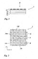
- Fig. 2 now shows in detail the formation of the metallic layer 14 in plan view.
- the metallic layer 14 is subdivided into island-shaped regions 14m, which are respectively enclosed by demetallized regions 14d of the replication layer 12 with a width B.
- the demetallized areas 14d form a contiguous background area.
- the regions 14m are arranged in a grid with a screen width D, wherein the grid lines are designated position 14r.
- You are in the Fig. 2 illustrated embodiment formed as square fields with an edge length F, which is smaller than the grid width D: F D - B
- the metallized areas 14m may be formed as reflecting surfaces, so that the film body 1 appears as a mirror film.
- diffractive optical structures into the regions 14m, for example a hologram, or matt structures can be formed.
- a variety of optical effects can be generated that go beyond the replica of an optically uniform metallic surface.
- "metallic" microwaveable safety features, logos or labels can be placed on finished-meal packages that are not destroyed when heated in the microwave because they are electrically non-conductive metallic surfaces.
- Security elements such as those used on documents and bills, can be equipped in this way with an additional security feature, which consists in that such a security element is not destructible by microwave radiation.
- electronic devices such as television receivers can be provided with an electrically non-conductive metallic surface.
- the metal layer does not have to come to rest on the physical surface, but may also be embedded between dielectric layers, for example as part of a transfer layer or by injection molding in the manufacture of the housing components.
- the grid of in Fig. 2 illustrated embodiment is a square grid, whose grid width D in the coordinate directions x and y is the same, but can also be provided that the grid width D in the direction of the x-coordinate and the y-coordinate is different.
- the edge length F of the metallized region 14m and / or the width B of the demetallized region 14d may be formed differently.
- the metallized areas 14m may also be rectangular, circular, elliptical or otherwise shaped Areas with closed contour act. For a square grid, as in Fig. 2 As illustrated, squares, circles, and regular polygons may be preferred as the contour of the metallized regions.
- line-shaped metallized regions 14m which are separated from each other by line-shaped demetallized regions 14d.
- the metallized areas 14m are thus arranged in a line grid, i. in a one-dimensional grid.
- Such a film body is consequently made to be insulating in a direction perpendicular to the line-shaped regions 14m, 14d and to be conductive in a direction parallel to the line-shaped regions 14m, 14d.
- Fig. 3 now shows a second embodiment in which the screen width in a random manner by ⁇ 40% by the value D 0 varies. It is in Fig. 3 around a film body 2 shown in plan view, in which both the metallized regions 14m and the demetallized regions 14d are formed irregularly shaped, wherein the deviations from a square grid are not larger than 40%. With such an embodiment, for example, the occurrence of moiré effects or disturbing diffraction effects can be avoided.
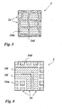
- Fig. 4 shows a schematic representation of a third embodiment, which by varying the first embodiment in Fig. 2 is formed.
- a metallic layer 34 is now structured such that, in addition to mutually insulated metallized regions 34m, regions of the metallic layer 34 are connected to one another and thus form conductor tracks 34l.
- antennas can be formed that are not visible to the unaided human eye.
- those under the metallized Regions 34m, 341 arranged replicating layer may have a diffraction-optical relief structure, for example in the form of a hologram, so also security elements can be provided with electrical functional elements.
- the film body of such a security element can have further layers which, for example, form an RFID tag, ie a circuit which serves for identification by means of radio waves.
- the background region that is to say between the metallized regions 34m, 34l, can be filled with an opaque colored layer.
- Fig. 5 shows a fourth embodiment, in which a film 4 applied to a metallic layer 44 is formed as a substantially transparent electrically conductive layer.
- a film 4 applied to a metallic layer 44 is formed as a substantially transparent electrically conductive layer.
- island-shaped demetallized areas 44d are now surrounded by metallized strip-shaped areas 44m, which are connected to one another and thus form a coherent electrically conductive surface area.
- This surface area has the form of a close meshed network.
- the metallic layer 44 may be used, for example, as a shield against electromagnetic fields or for the discharge of static charges.
- the foil body 4 in the demetallized areas 44d may have a transparent colored layer in register with the strip-shaped metallic areas 44m. For better orientation are in Fig. 5 the grid lines 14r drawn (see. Fig. 2 ).
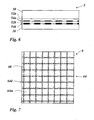
- Fig. 6 now shows a film body 5, which consists of a carrier layer 50, a first replication layer 52a, a first metallic layer 54a, a second replication layer 52b, a second metallic layer 54b and an adhesive layer 56.
- the two metallic layers 54a and 54b are arranged at such a distance from each other that the known interference effects can occur on thin layers.
- the two metallic layers 54a and 54b also have different thicknesses.
- the metallic layer 54a arranged closer to the carrier layer 50 is the thinner layer. It has a thickness in the lower nanometer range, so that it appears partially transparent in visible light. Because the transparency of a thin metal layer is inter alia dependent on the material, the required layer thickness is expediently determined by a series of experiments.
- Fig. 7 shows a film body 6 in plan view, in which the surface in the manner described above has island-shaped metallized areas 64m, which are surrounded by the metallized areas 64d.
- a micro-marking is introduced, which is formed in the illustrated embodiment as a micro-font, which is readable only with an optical aid, such as a strong magnifying glass or a microscope. But it can also be provided micrographics.
- the micro tag can reduce the electrical flashover strength of the demetallized regions 64d, provided that it has a metallized surface.
- the described embodiments include that the partial demetallization of the metallic layer occurs in the register.
- the metallic layer is arranged on the replication layer, which has a surface profile at least in regions. If now on the replication a metallic layer with uniform Surface density is applied based on the plane spanned by the replication layer, for example by vapor deposition in vacuum, the surface density or layer thickness can be chosen so that the applied metallic layer, depending on the local depth-to-width ratio of the surface profile a different has optical density. If the metallic layer is then used as an exposure mask for a photoresist, ie the photoresist is exposed through the metallic layer, then it can be developed into a register-accurate etching mask and the metallic layer can be partially demetallised in register.
- a surface profile with a high depth-to-width ratio for example with a depth-to-width ratio> 2
- the surface area profile can be formed into the regions of the replication layer arranged below the demetallized regions Replication layer under the metallized areas have a very low depth-to-width ratio .
- the dimensionless depth-to-width ratio is a characteristic feature of the surface enlargement, preferably of periodic structures.
- Such a structure forms “mountains” and “valleys” in a periodic sequence.
- Depth is here the distance between “mountain” and “valley”, as width the distance between two “mountains”.
- This effect can also be observed in the case of discretely distributed "valleys", which can be arranged at a distance that is many times greater than the depth of the "valleys".
- the depth of the "valley” is the width of the "valley” in order to properly describe the geometry of the "valley” by specifying the depth-to-width ratio.
- silver and gold As can be seen, have a high maximum reflectance R max and require one relatively small depth-to-width ratio for forming transparency.
- aluminum Al also has a high maximum reflectance R Max , it requires a higher depth-to-width ratio.
- it may be provided to form the metal layer of silver or gold. But it can also be provided to form the metal layer of other metals or of metal alloys.
- Table 2 now shows the calculation results obtained from rigorous diffraction calculations for surface structures formed as linear, sinusoidal grids with a grid spacing of 350 nm with different depth-to-width ratios.
- the degree of transparency, apart from the depth-to-width ratio depends on the polarization of the light radiated.
- the degree of transparency or the reflectance of the metal layer is wavelength-dependent. This effect is especially good for TE polarized light.
- the degree of transparency decreases when the angle of incidence of the light differs from the normal angle of incidence, i. the degree of transparency decreases when the light is not incident vertically.
- the metal layer in the region of the surface structure can be made transparent only in a limited incidence cone of the light. It can therefore be provided that the metal layer is formed opaque when viewed obliquely, this effect is useful for the use of the metal layer as a selective exposure mask.
- the Fig. 8 to 10 Now show an embodiment for producing a passergenau teildemetallêten metallic layer.
- Fig. 8 shows a multilayer film body 81, which is like that in Fig. 1 described film body 1 is constructed.
- the film body 81 consists of several layers. In the exemplary embodiment shown, these are a carrier foil 80, a replication layer 82 and a metallic layer 84, as well as an adhesive layer 86, which is applied to the side of the carrier foil 80 facing away from the replication layer 82.
- a photosensitive layer 88 is applied on the metallic layer 84.
- the photosensitive layer 88 may be, for example, a UV-sensitive photoresist. This may be an organic layer which is applied in liquid form by conventional coating methods, such as gravure printing. It may also be provided that the photosensitive layer is vapor-deposited or laminated as a dry film.
- Fig. 11 shows the exposure of the photosensitive layer 88 from the side of the adhesive layer 86 with the photosensitive layer 88 being in the developed state.
- the exposure of the photosensitive layer 88 is provided with UV light 89, the metallic layer 84 acting as an exposure mask.
- the photosensitive layer 88 has areas 88u in which the layer 88 is obtained and areas 88b in which the layer 88 is removed as a result of development.
- the areas 88u are areas where the replication layer 82 is formed with a lower depth-to-width ratio-in the illustrated embodiment, it is zero-while in the areas 88b, the replication layer 88 has a surface texture has a high depth-to-width ratio.
- the metallic layer 84 is formed with a smaller thickness than in the areas 88u, so that the metallic layer 84 has a different transmission in both areas and thus the incident UV light is attenuated to varying degrees. It is not necessary to make the metallic layer so thin that the regions 88b appear transparent when viewed visually. A relatively low total transmission of the film body 81 can be compensated by an increased exposure dose of the photosensitive layer 88. It should also be noted that the exposure of the photosensitive Layer is typically provided in the near UV range, so that the visual viewing impression for the assessment of the transmission is not critical.
- the photosensitive layer 88 is formed of a positive photoresist.
- the exposed areas are soluble in the developer.
- the unexposed areas are soluble in the developer. It is possible in this way to demetall matters with a layout different areas of the metallic layer 84 register accurate. It may further be provided to further modify the metallic layer 84 with the aid of a subsequent galvanic treatment, for example to form it with increased layer thickness, for example conductor tracks as described above Fig. 4 shown to form with improved electrical conductivity.
- Fig. 10 now shows the film body 81 in its final state, after using an etchant, the metallic layer 84 is removed in the areas 88b.
- the metallic layer 84 is therefore only present in the regions 88u and thus forms electrically isolated islands from one another.
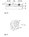
- Fig. 11 now shows a multi-layer body 110, which is divided into island areas 114 in a random manner.
- raster lines 114r are also randomly arranged and formed.
- the grid lines 114r are formed as a straight line. But they can also be curved lines. It can further be provided that the lines are formed with varying width.
- the grid width D and the width B are determined as mean values over all island areas 114.
- the size and shape of the island regions 114 may vary within a wide range, as well as the location of the centroids of the island regions. Nevertheless, it is envisaged that the island regions will typically have a mean size ⁇ 250 ⁇ m and the ratio between mean island size and width of the breaks will be between 5 and 200.
- the island regions 114 may be metallized and the background region characterized by the raster lines 114r may be demetallized or vice versa.
Description
Die Erfindung betrifft einen Mehrschichtkörper mit einer Replizierschicht, die mikroskopisch feine Musterbereiche aufweist, sowie ein Verfahren zur Herstellung eines Mehrschichtkörpers mit einstellbarer bzw. definierter elektrischer Leitfähigkeit.The invention relates to a multilayer body having a replication layer which has microscopically fine pattern areas, and to a method for producing a multilayer body having adjustable or defined electrical conductivity.
Es sind metallisierte Mehrschichtkörper, insbesondere metallisierte Folien bekannt, die eine spiegelnde oder matte oder sonstwie strukturierte Oberfläche aufweisen, die elektrisch leitend ist. Die elektrisch leitende Oberfläche kann störend sein, beispielsweise wenn die Folien zur Dekoration von Gehäusen elektronischer Geräte vorgesehen sind oder wenn die Folien als Verpackung für Lebensmittel dienen sollen, die der elektromagnetischen Strahlung eines Mikrowellenherdes ausgesetzt wird. Solche Verpackungen können zugleich Sicherheitsmerkmale mit metallischer Oberfläche enthalten, die ebenfalls durch Mikrowellenstrahlung thermisch zerstört werden können.There are known metallized multilayer bodies, in particular metallized films, which have a reflective or matt or otherwise structured surface which is electrically conductive. The electrically conductive surface may be troublesome, for example when the foils are intended to decorate enclosures of electronic equipment, or when the foils are to serve as packaging for food exposed to the electromagnetic radiation of a microwave oven. Such packaging can also contain security features with a metallic surface, which can also be thermally destroyed by microwave radiation.
Der Erfindung liegt nun die Aufgabe zugrunde, einen Mehrschichtkörper mit einstellbarer bzw. definierter elektrischer Leitfähigkeit anzugeben sowie ein Herstellungsverfahren dazu, das kostengünstig und für Massenproduktion geeignet ist.The invention is based on the object of specifying a multi-layer body with adjustable or defined electrical conductivity and a manufacturing method that is cost-effective and suitable for mass production.
Die Aufgabe der Erfindung wird mit einem Verfahren zur Herstellung eines Mehrschichtkörpers mit einstellbarer bzw. definierter elektrischer Leitfähigkeit gelöst, wobei vorgesehen ist, daß in einem ersten Bereich einer Replizierschicht des Mehrschichtkörpers eine diffraktive erste Oberflächenstruktur abgeformt wird, daß eine metallische Schicht auf die Replizierschicht in dem ersten Bereich und in einem zweiten Bereich, in dem die erste Oberflächenstruktur nicht in die Replizierschicht abgeformt ist, aufgebracht wird, wobei entweder der erste Bereich oder der zweite Bereich von einer Vielzahl mikroskopisch feiner Musterbereiche gebildet wird, die in einem Linienraster oder in einem Flächenraster mit der Rastenrveite D angeordnet sind und die jeweils durch den, jeden der Teilbereiche vollständig begrenzenden oder umschließenden zweiten Bereich bzw. ersten Bereich voneinander getrennt in einem Abstand B voneinander angeordnet sind, daß auf die metallische Schicht eine photoempfindliche Schicht aufgebracht wird oder als Replizierschicht eine photoempfindliche Waschmaske aufgebracht wird, daß die photoempfindliche Schicht bzw. Waschmaske durch die metallische Schicht hindurch belichtet wird, so daß die photoempfindliche Schicht bzw. Waschmaske durch die erste Oberflächenstruktur bedingt im ersten und im zweiten Bereich unterschiedlich belichtet wird, und daß die metallische Schicht unter Verwendung der belichteten photoempfindlichen Schicht bzw. Waschmaske als Maskenschicht im ersten Bereich, nicht jedoch im zweiten Bereich, oder im zweiten Bereich, nicht jedoch im ersten Bereich entfernt wird.The object of the invention is achieved with a method for producing a multilayer body with adjustable or defined electrical conductivity, wherein it is provided that in a first region of a replication layer of the multilayer body, a diffractive first surface structure is formed, that a metallic layer on the replication in the first region and in a second region in which the first surface structure is not formed in the replication layer, wherein either the first region or the second region is formed by a plurality of microscopically fine pattern areas, in a line grid or in a surface grid with the Rastenrveite D are arranged and which are each separated by the, each of the sub-areas completely delimiting or enclosing the second area or first area separated from each other at a distance B from each other that on the metallic layer a photoemp is applied sensitive layer or as a replication layer, a photosensitive wash mask is applied, that the photosensitive layer or wash mask is exposed through the metallic layer, so that the photosensitive layer or washing mask is exposed differently by the first surface structure in the first and in the second region and that the metallic layer is removed using the exposed photosensitive layer or mask as a mask layer in the first region, but not in the second region, or in the second region, but not in the first region.
Die Aufgabe wird weiter mit einem Mehrschichtkörper, insbesondere einer Transferfolie, mit einer Replizierschicht und einer auf der Replizierschicht angeordneten metallischen Schicht gelöst, wobei vorgesehen ist, daß der Mehrschichtkörper eine Vielzahl mikroskopisch feiner Musterbereiche und einen jeden der Musterbereiche vollständig begrenzenden oder umschließenden Hintergrundbereich aufweist, wobei die Musterbereiche in einem Linienraster oder in einem Flächenraster mit der Rasterweite D angeordnet sind, die Musterbereiche jeweils durch den Hintergrundbereich voneinander getrennt in einem Abstand B voneinander angeordnet sind, die Rasterweite D kleiner als 500 µm ist und das Verhältnis der Rasterweite D zum Abstand B im Bereich von 5 bis 200 liegt, und daß die metallische Schicht entweder im Hintergrundbereich oder in den Musterbereichen entfernt ist.The object is further achieved with a multi-layer body, in particular a transfer film, with a replication layer and a metallic layer arranged on the replication layer, wherein it is provided that the multi-layer body has a multiplicity of microscopically fine pattern areas and a background area completely delimiting or enclosing the pattern areas the pattern areas are arranged in a line grid or in an area grid with the screen width D, the pattern areas are separated from each other by the background area at a distance B from one another, the screen pitch D is smaller than 500 μm, and the ratio of the grid spacing D to the distance B in FIG Range of 5 to 200, and that the metallic layer is removed either in the background area or in the pattern areas.
Es ist also vorgesehen, daß zur Herstellung von an einem Raster ausgerichteten, mikroskopisch feinen Inselstrukturen die auf die Oberflächenstruktur aufgebrachte metallische Schicht selbst eine optische Belichtungsmaske bildet, wobei die optische Wirkung der metallischen Schicht jeweils durch die Oberflächenstruktur bestimmt ist, auf der sie angeordnet ist. Auf diese Weise kann eine registerhaltige teilweise Entfernung der als Belichtungsmaske fungierenden metallischen Schicht selbst erzielt werden, und zwar in der hohen Auflösung und Qualität, die für die Herstellung der mikroskopisch feinen Inselstrukturen erforderliche ist.It is thus envisaged that for the production of microscopically fine island structures aligned on a grid, the metallic layer applied to the surface structure itself forms an optical exposure mask, the optical effect of the metallic layer being determined by the surface structure on which it is arranged. In this way, in-register partial removal of the metallic layer itself acting as an exposure mask can be achieved, in the high resolution and quality required to fabricate the microscopically fine island structures.
Der Begriff "Raster" wird hier nicht nur als gleichmäßige Unterteilung einer Fläche gebraucht. Vielmehr sind auch ungleichmäßige oder zufällige Raster, wie beispielsweise frequenzmodulierte Raster, wie sie in der Druckindustrie verwendet werden, unter "Raster" verstanden. Es sind also ausdrücklich Unterteilungen der Fläche in Inselbereiche eingeschlossen, die völlig stochastisch gebildet sind. Die Linien zwischen den Inselbereichen können auch gekrümmt sein und/oder von variierender Dicke sein. Bei der Rasterweite D und/oder dem Abstand B kann es sich auch um Mittelwerte der Gesamtheit handeln. Weiter kann es sich um Linienraster, d.h. um eindimensionale Raster oder um mehrdimensionale Raster handeln, beispielsweise um Flächenraster.The term "grid" is not only used here as a uniform subdivision of a surface. Rather, uneven or random grids, such as frequency-modulated grids, as used in the printing industry, understood by "raster". Thus, it is expressly included subdivisions of the area in island areas, which are formed completely stochastic. The lines between the island areas can also be curved and / or be of varying thickness. The grid width D and / or the distance B can also be average values of the totality. Furthermore, they can be line grids, ie one-dimensional grids or multi-dimensional grids, for example area grids.
Durch die Erfindung wird somit ein Herstellungsverfahren für partiell metallisierte Mehrschichtkörper, insbesondere partiell metallisierte Folien mit mikroskopisch feinen Inselstrukturen angegeben, welches besonders effektiv und kostengünstig ist.The invention thus provides a production method for partially metallized multilayer bodies, in particular partially metallized foils with microscopically fine island structures, which is particularly effective and inexpensive.
Durch die besondere Strukturierung eines erfindungsgemäßen Mehrschichtkörpers werden weiter folgende Vorteile erzielt:The special structuring of a multilayer body according to the invention further achieves the following advantages:
Diese Strukturierung ist durch das unbewaffnete menschliche Auge nicht wahrnehmbar. So erscheint die metallische Schicht eines erfindungsgemäßen Mehrschichtkörpers, der mit der oben spezifizierten Anordnung von metallisierten inselförmigen Musterbereiche versehen ist, dem unbewaffneten menschlichen Auge einerseits als homogene metallische Oberfläche. Andererseits ist die metallische Schicht elektrisch nicht leitfähig, jedoch durchgängig für elektromagnetische Strahlung bis hin zum Mikrowellenbereich. Der Mehrschichtkörper kann deshalb beispielsweise der Strahlung einer Mikrowelle ausgesetzt werden, ohne sich merklich zu erhitzen. Damit ist mittels des erfindungsgemäßen Mehrschichtkörpers eine metallisch erscheinende, aber elektrisch nicht leitfähige Oberfläche realisierbar. Durch geeignete Ausgestaltung der Parameter, wie beispielsweise Rasterweite D und/oder Abstand B der Musterbereiche und/oder der Art des Rasters kann zudem der Effekt der elektrischen Leitfähigkeit frequenzabhängig gestaltet werden. Dies bedeutet, dass je nach Anregungsfrequenz eine elektrische Leitfähigkeit vorliegen kann oder nicht.This structuring is imperceptible to the unaided human eye. Thus, the metallic layer of a multilayer body according to the invention, which is provided with the above-specified arrangement of metallized island-shaped pattern areas, appears to the unarmed human eye as a homogeneous metallic surface. On the other hand, the metallic layer is electrically non-conductive, but throughout for electromagnetic radiation up to the microwave range. The multilayer body can therefore be exposed to, for example, the radiation of a microwave without noticeably heating. Thus, by means of the multilayer body according to the invention a metallically appearing, but electrically non-conductive surface can be realized. By suitable design of the parameters, such as grid spacing D and / or distance B of the pattern areas and / or the type of grid, moreover, the effect of the electrical conductivity can be made frequency-dependent. This means that depending on the excitation frequency, an electrical conductivity may or may not be present.
Wenn es sich beispielsweise bei den Musterbereichen um spiegelnde Bereiche handelt, wird ein als Folie ausgebildeter Mehrschichtkörper als eine metallische Spiegelfolie wahrgenommen. Eine solche Folie kann beispielsweise zur Dekoration von elektrischen Geräten, wie etwa Fernsehempfängern, verwendet werden, die eine elektrisch nichtleitende Oberfläche aufweisen sollen.For example, if the pattern areas are specular areas, a multilayer body formed as a film is perceived as a metallic mirror film. Such a film can be used, for example, for the decoration of electrical appliances, such as television receivers, which are to have an electrically non-conductive surface.
Andererseits kann durch Variation der Oberflächenstruktur eine transparente Folie hergestellt werden, die eine elektrisch leitende Oberfläche aufweist. Eine solche elektrisch leitfähige Folie kann beispielsweise demetallisierte Musterbereiche aufweisen, die von einem metallisierten Hintergrundbereich umgeben sind. Diese Folie kann beispielsweise als transparente Abschirmfolie verwendet werden, die trotz ihrer Transparenz wegen des netzartig ausgebildeten metallisierten Hintergrundbereichs elektromagnetische Strahlung abzuschirmen oder statische elektrische Ladungen abzuleiten vermag.On the other hand, by varying the surface structure, a transparent film having an electrically conductive surface can be produced. Such an electrically conductive film may have, for example, demetallized pattern areas which are surrounded by a metallized background area. This film can be used, for example, as a transparent shielding film, which despite its transparency because of the reticulated metallized background region to shield electromagnetic radiation or is able to dissipate static electrical charges.
Beliebige elektrische Leitfähigkeiten lassen sich beispielsweise durch Variation der Schichtdicke der metallischen Schicht oder durch Variation des Verhältnisses D/B einstellen.Any electrical conductivities can be adjusted, for example, by varying the layer thickness of the metallic layer or by varying the ratio D / B.
Wenn ein Linienraster vorgesehen ist, kann beispielsweise ein Mehrschichtkörper als eine Folie ausgebildet werden, die isolierend in einer Richtung und leitend in einer anderen Richtung ist.For example, when a line grid is provided, a multilayer body may be formed as a film which is insulating in one direction and conducting in another direction.
Vorteilhafte Ausgestaltungen sind in den Unteransprüchen bezeichnet.Advantageous embodiments are designated in the subclaims.
Vorzugsweise kann vorgesehen sein, daß die Rasterweite D im Bereich von 1 µm bis 500 µm gewählt wird, bevorzugt im Bereich von 5 µm bis 300 µm gewählt wird. Es kann auch vorgesehen sein, daß die Rasterweite im Bereich von 10 µm bis 250 µm liegt. Wenn die Rasterweite D in diesen Bereichen liegt, werden einerseits auffällige Beugungseffekte des Mehrschichtkörpers vermieden und andererseits sind die Musterbereiche im einzelnen nicht sichtbar, da die Unterteilung unterhalb der Auflösungsgrenze des unbewaffneten menschlichen Auges liegt.Preferably, it can be provided that the screen width D is selected in the range of 1 .mu.m to 500 .mu.m, preferably in the range of 5 .mu.m to 300 .mu.m. It can also be provided that the grid width in the range from 10 μm to 250 μm. If the screen width D is in these ranges, conspicuous diffraction effects of the multilayer body are avoided on the one hand, and on the other hand the pattern areas are not visible in detail since the subdivision lies below the resolution limit of the unarmed human eye.
Weiter kann vorgesehen sein, daß das Verhältnis der Rasterweite D zum Abstand B im Bereich von 5 bis 200 gewählt wird. Mit dem Verhältnis D/B kann insbesondere die elektrische Durchschlagsfestigkeit des Mehrschichtkörpers beeinflußt werden.It can further be provided that the ratio of the grid width D to the distance B in the range of 5 to 200 is selected. With the ratio D / B, in particular the electrical breakdown strength of the multilayer body can be influenced.
. Es ist vorgesehen, daß die metallische Schicht auf eine von der Replizierschicht aufgespannte Ebene vollflächig in einer konstanten Flächendichte aufgebracht, vorzugsweise aufgedampft wird. Ein solches Verfahren ist kostengünstig und in der Schichtdicke der metallischen Schicht gut steuerbar., It is envisaged that the metallic layer is applied to a plane spanned by the replication layer over its entire surface in a constant areal density, preferably vapor-deposited. Such a method is inexpensive and well controllable in the layer thickness of the metallic layer.
In einer vorteilhaften Ausgestaltung ist vorgesehen, daß die metallische Schicht auf die Replizierschicht vollflächig in einer Dicke aufgebracht wird, bei der die metallische Schicht in einem Bereich der Replizierschicht ohne Oberflächenstruktur eine optische Dichte zwischen 1 und 7 besitzt. Der Effekt der unterschiedlichen Transmission, insbesondere Transparenz wird durch das weiter unten näher beschriebene Tiefen-zu-Breiten-Verhältnis der Oberflächenstruktur der Replizierschicht eingestellt. Bei der metallischen Schicht kann es sich um ein Metall, beispielsweise um Aluminium, Silber, Gold, Kupfer, Chrom oder Palladium oder um eine Legierung aus diesen und/oder weiteren Metallen handeln oder um eine Schichtfolge der oben aufgeführten Metalle.In an advantageous embodiment, it is provided that the metallic layer is applied to the replication completely over the entire surface in a thickness at which the metallic layer has an optical density of between 1 and 7 in a region of the replication layer without a surface structure. The effect of the different transmission, in particular transparency, is set by the depth-to-width ratio of the surface structure of the replication layer described in more detail below. The metallic layer may be a metal, for example aluminum, silver, gold, copper, chromium or palladium, or an alloy of these and / or other metals, or a layer sequence of the metals listed above.
Es kann weiter vorgesehen sein, daß in dem zweiten Bereich eine zweite Oberflächenstruktur in der Replizierschicht abgeformt ist und daß als erste diffraktive Oberflächenstruktur eine Oberflächenstruktur in die Replizierschicht abgeformt wird, die die Transmission, insbesondere die Transparenz der metallischen Schicht im ersten Bereich gegenüber der Transmission, insbesondere der Transparenz der metallischen Schicht in dem zweiten Bereich erhöht, oder umgekehrt. Auf diese Weise kann also mittels der Oberflächenstruktur in der Replizierschicht die Transmission, insbesondere die Transparenz, bzw. die optische Dichte der metallischen Schicht beeinflußt werden. Bereits geringe Unterschiede in der Transmission oder Transparenz, die beispielsweise durch das menschliche Auge nicht mehr wahrnehmbar sind, können bei geeigneten Fertigungsbedingungen ausreichend sein, um die metallische Schicht als Belichtungsmaske zu verwenden. Weil die Replizierschicht kostengünstig mit einer sehr feinen Oberflächenstruktur ausgebildet werden kann, lassen sich die geforderten hohen Auflösungen bei der Teildemetallisierung der metallischen Schicht ebenso kostengünstig ausführen.It can further be provided that in the second region a second surface structure is formed in the replication layer and that a surface structure is formed in the replication layer as the first diffractive surface structure, the transmission, in particular the transparency of the metallic layer in the first region relative to the transmission, in particular, increases the transparency of the metallic layer in the second region, or vice versa. In this way, the transmission, in particular the transparency, or the optical density of the metallic layer can thus be influenced by means of the surface structure in the replication layer. Even slight differences in transmission or transparency, which are no longer perceptible, for example, by the human eye, may be sufficient under suitable production conditions to use the metallic layer as an exposure mask. Because the replication layer can be inexpensively formed with a very fine surface structure, the required high resolutions in the partial demetallization of the metallic layer can also be carried out inexpensively.
Es kann vorgesehen sein, daß die erste Oberflächenstruktur eine größere Relieftiefe als die zweite Oberflächenstruktur besitzt oder umgekehrt.It can be provided that the first surface structure has a greater relief depth than the second surface structure or vice versa.
In einer weiteren Ausführung kann vorgesehen sein, daß das Produkt aus Spatialfrequenz und Relieftiefe der ersten Oberflächenstruktur größer als das Produkt aus Spatialfrequenz und Relieftiefe der zweiten Oberflächenstruktur ist oder umgekehrt. Die Spatialfrequenz wird in Linien/mm angegeben und ist ein kennzeichnendes Merkmal für diffraktive Strukturen. Bei der bevorzugten Rasterweite von 5 µm bis 300 µm ist sie vorteilhafterweise zwischen 500 Linien/mm und 5000 Linien/mm gewählt. Bei Strukturen mit stochastischem Profil, wie beispielsweise Mattstrukturen, wird als Kenngröße eine typische Distanz zwischen Erhebungen verwendet oder beispielsweise die sogenannte Korrelationslänge. Diese Kenngröße liegt analog zwischen 0,2 und 2,0 µm.In a further embodiment it can be provided that the product of Spatialfrequenz and relief depth of the first surface structure is greater than the product of Spatialfrequenz and relief depth of the second surface structure or vice versa. The spatial frequency is given in lines / mm and is a characteristic feature of diffractive structures. In the preferred screen width of 5 microns to 300 microns, it is advantageously chosen between 500 lines / mm and 5000 lines / mm. In structures with stochastic profile, such as matte structures, is a typical characteristic Distance between surveys used or, for example, the so-called correlation length. This parameter is analogously between 0.2 and 2.0 microns.
Es kann vorgesehen sein, daß in dem ersten Bereich als erste diffraktive Oberflächenstruktur eine Oberflächenstruktur mit einem hohem Tiefen-zu-Breiten-Verhältnis der einzelnen Strukturelemente, insbesondere mit einem Tiefen-zu-Breiten-Verhältnis > 0,3, abgeformt wird und daß die zweite Oberflächenstruktur als Oberflächenstruktur mit niedrigerem Tiefen-zu-Breiten-Verhältnis ausgebildet wird, oder umgekehrt.It can be provided that in the first region as the first diffractive surface structure, a surface structure having a high depth-to-width ratio of the individual structural elements, in particular with a depth-to-width ratio> 0.3, is molded and that the second surface structure is formed as a surface structure with a lower depth-to-width ratio, or vice versa.
Das dimensionslose Tiefen-zu-Breiten-Verhältnis, häufig auch als Aspektrate bezeichnet, ist ein kennzeichnendes Merkmal für die Oberflächenvergrößerung durch vorzugsweise periodische Strukturen. Eine solche Struktur bildet in periodischer Abfolge "Berge" und "Täler" aus. Als Tiefe ist hier der Abstand zwischen "Berg" und "Tal" bezeichnet, als Breite der Abstand zwischen zwei "Bergen". Je höher nun das Tiefen-zu-Breiten-Verhältnis ist, desto steiler sind die "Bergflanken" ausgebildet und desto dünner ist eine auf den "Bergflanken" abgeschiedene metallische Schicht ausgebildet. Dieser Effekt ist auch zu beobachten, wenn es sich um diskret verteilte "Täler" handelt, die in einem Abstand zueinander angeordnet sein können, der um ein Vielfaches größer als die Tiefe der "Täler" ist. In einem solchen Fall ist die Tiefe des "Tales" zur Breite des "Tales" ins Verhältnis zu setzen, um durch Angabe des Tiefen-zu-Breiten-Verhältnisses die Geometrie des "Tales" zutreffend zu beschreiben.The dimensionless depth-to-width ratio, often referred to as aspect ratio, is a characteristic feature of surface enlargement by preferably periodic structures. Such a structure forms "mountains" and "valleys" in a periodic sequence. Depth is here the distance between "mountain" and "valley", as width the distance between two "mountains". The higher the depth-to-width ratio is, the steeper the "mountain flanks" are formed and the thinner a metallic layer deposited on the "mountain flanks" is formed. This effect can also be observed in the case of discretely distributed "valleys", which can be arranged at a distance that is many times greater than the depth of the "valleys". In such a case, the depth of the "valley" should be related to the width of the "valley" to properly describe the geometry of the "valley" by specifying the depth-to-width ratio.
Es ist also möglich, mit Hilfe des Tiefen-zu-Breiten-Verhältnisses die effektive Dicke der metallischen Schicht im Bereich der Oberflächenstruktur einzustellen.It is thus possible to adjust the effective thickness of the metallic layer in the area of the surface structure by means of the depth-to-width ratio.
Weitere vorteilhafte Ausführungen sind auf die Gestaltung der Belichtung und Entwicklung der photoempfindlichen Schichten sowie auf das Ätzen der metallischen Schicht gerichtet.Further advantageous embodiments are directed to the design of the exposure and development of the photosensitive layers and to the etching of the metallic layer.
Es kann vorgesehen sein, daß als photoempfindliche Schicht oder als photoempfindliche Waschmaske ein photoempfindliches Material mit einer binären Charakteristik aufgebracht wird und daß die photoempfindliche Schicht bzw. die photoempfindliche Waschmaske durch die metallische Schicht hindurch in einer Belichtungsstärke und Belichtungsdauer belichtet wird, daß die photoempfindliche Schicht bzw. die photoempfindliche Waschmaske im ersten Bereich oder im zweiten Bereich, in dem die Transmission, insbesondere die Transparenz der metallischen Schicht durch die erste Oberflächenstruktur bedingt erhöht ist, aktiviert wird und im zweiten Bereich nicht aktiviert wird, oder umgekehrt.It can be provided that a photosensitive material having a binary characteristic is applied as the photosensitive layer or as a photosensitive wash mask and that the photosensitive layer or the photosensitive wash mask is exposed through the metallic layer in an exposure intensity and exposure time such that the photosensitive layer or photosensitive layer is exposed the photosensitive washing mask in the first region or in the second region, in which the transmission, in particular the transparency of the metallic layer is conditionally increased by the first surface structure, is activated and is not activated in the second region, or vice versa.
Dabei kann vorgesehen sein, daß die photoempfindliche Schicht bzw. Waschmaske durch die metallische Schicht hindurch mittels UV-Strahlung belichtet wird. UV-Strahlung ist energiereicher als Tageslicht und deshalb vielfach bevorzugt.It can be provided that the photosensitive layer or washing mask is exposed through the metallic layer by means of UV radiation. UV radiation is more energetic than daylight and therefore often preferred.
Anschließend können die durch die Belichtung aktivierten Bereiche der photoempfindlichen Waschmaske und die darauf angeordneten Bereiche der metallischen Schicht in einem Waschprozeß entfernt werden.Subsequently, the areas of the photosensitive washing mask activated by the exposure and the areas of the metallic layer arranged thereon can be removed in a washing process.
Es kann aber auch vorgesehen sein, daß die belichtete photoempfindliche Schicht entwickelt wird und daß die entwickelte photoempfindliche Schicht eine Ätzmaske für die metallische Schicht bildet.However, it may also be provided that the exposed photosensitive layer is developed and that the developed photosensitive layer forms an etching mask for the metallic layer.
Eine weitere vorteilhafte Ausgestaltung sieht vor, daß die photoempfindliche Schicht durch die Belichtung im ersten Bereich, in dem die Transmission, insbesondere die Transparenz der metallischen Schicht durch die erste Oberflächenstruktur erhöht ist, aktiviert wird, und daß die aktivierte photoaktivierbare Schicht ein Ätzmittel für die metallische Schicht bildet.A further advantageous embodiment provides that the photosensitive layer is activated by the exposure in the first region in which the transmission, in particular the transparency of the metallic layer is increased by the first surface structure, and that the activated photoactivatable layer is an etchant for the metallic Layer forms.
Es kann vorgesehen sein, daß die photoempfindliche Schicht aus einem Photoresist ausgebildet wird.It may be provided that the photosensitive layer is formed of a photoresist.
Der Photoresist kann als positiver Photoresist oder als negativer Photoresist ausgebildet werden.The photoresist may be formed as a positive photoresist or as a negative photoresist.
Bei der photoempfindlichen Schicht kann es sich auch um ein Photopolymer handeln.The photosensitive layer may also be a photopolymer.
Es kann weiter vorgesehen sein, daß die Überreste der Ätzmasken entfernt werden.It may further be provided that the remnants of the etching masks are removed.
Ein möglicher Ausgangspunkt zur Herstellung des teilmetallisierten Mehrschichtkörpers ist also die metallische Schicht, welche mit einem Photoresist beschichtet ist. Die Strukturierung erfolgt typischerweise, wie oben beschrieben, durch Belichtung des Photoresists, Entwickeln bzw. Ätzen des Photoresists und Ätzen der metallischen Schicht mit dem Photoresist als Ätzmaske. Die Belichtung des Photoresists kann beispielsweise erfolgen durch:
- einen Bandbelichter; dabei wird eine bandförmige Belichtungsmaske in Kontakt mit dem Mehrschichtkörper transportiert und durch die Maske hindurch der Photoresist auf dem Mehrschichtkörper belichtet;
- angesteuertes Belichten mit einem fokussierten Laserstrahl, d.h. ein Laserstrahl wird durch eine Ansteuereinheit mittels einer Ablenkeinheit und ggf. einer Fokussieroptik über den Mehrschichtkörper bewegt;
- eine Maske, welche über eine Abbildungsoptik auf den Mehrschichtkörper projiziert wird. Das Verfahren kann im Sinne von "step & repeat" sein oder mittels einer im Register angesteuerten Blitzlampe erfolgen. Zudem kann die Maske elektronisch gesteuert und variabel sein, beispielsweise ein "spatial light modulator".
- a tape recorder; In this case, a band-shaped exposure mask is transported in contact with the multilayer body and exposed through the mask, the photoresist on the multilayer body;
- controlled exposure with a focused laser beam, ie a laser beam is moved by a drive unit by means of a deflection unit and possibly a focusing optics over the multilayer body;
- a mask which is projected onto the multilayer body via an imaging optic. The method may be in the sense of "step &repeat" or by means of a controlled in the register flash lamp. In addition, the mask can be electronically controlled and variable, for example a "spatial light modulator".
Vorteilhafterweise erfolgt die Belichtung jeweils auf die Photoresistseite, sie kann jedoch auch durch die metallische Schicht hindurch erfolgen.Advantageously, the exposure takes place in each case on the photoresist side, but it can also take place through the metallic layer.
Weiterhin kann die Strukturierung auch durch direkte Laserbestrahlung (Ablation) erfolgen, ohne den Umweg mittels Photoresist als "verstärker". Dabei kann unmittelbar das unterschiedliche Absorptionsverhalten der metallischen Schicht in Bereichen mit unterschiedlichen Oberflächenstrukturen bzw. in Bereichen mit und ohne Oberflächenstrukturen ausgenutzt werden.Furthermore, the structuring can also be done by direct laser irradiation (ablation), without the detour using photoresist as "amplifier". In this case, the different absorption behavior of the metallic layer in areas with different surface structures or in areas with and without surface structures can be exploited directly.
Weiterhin kann die Strukturierung durch Ausnutzung des strukturabhängigen Ätzverhaltens der metallischen Schicht erfolgen. Werden nämlich strukturierte Oberflächen mit einer metallischen Schicht bedampft und einem geeigneten Ätzmedium ausgesetzt, so erscheinen Bereiche mit hohem Aspektverhältnis nach einer bestimmten Zeit transparent, währenddem unstrukturierte Bereiche oder Bereiche mit geringem Aspektverhältnis immer noch weitgehend opak erscheinen. Ein derart zeitgesteuerter Ätzprozess endet beispielsweise dann, wenn in Bereichen der Replizierschicht mit Oberflächenreliefstruktur und effektiv dünnerer Schichtdicke der metallischen Schicht Transparenz erzeugt wurde, während in Bereichen der Replizierschicht ohne Oberflächenstruktur und effektiv dickerer Schichtdicke der metallischen Schicht noch eine opake metallische Schicht vorliegt. Die auch in den unstrukturierten Bereichen auftretende Ätzung der metallischen Schicht wird üblicherweise durch eine zu Beginn erhöhte optische Dichte der aufgedampften metallischen Schicht vorkompensiert. Als Anwendungsfall kann beispielsweise die Ausbildung eines Handygehäuses vorgesehen sein.Furthermore, the structuring can take place by utilizing the structure-dependent etching behavior of the metallic layer. Namely, if patterned surfaces are vapor-deposited with a metallic layer and exposed to a suitable etching medium, high aspect ratio regions appear transparent after a certain time, while unstructured regions or low aspect ratio regions still appear largely opaque. Such a time-controlled etching process ends, for example, when in regions of the replication layer with surface relief structure and effectively thinner layer thickness of the metallic layer transparency was generated, while in regions of the replication without surface structure and effectively thicker layer thickness of the metallic layer still opaque metallic layer is present. The etching of the metallic layer which also occurs in the unstructured regions is usually precompensated by an initially increased optical density of the vapor-deposited metallic layer. As an application example, the formation of a mobile phone housing may be provided.
Weiter kann die Kombination mit klassischen Demetallisierungsverfahren vorgesehen sein. Es kann also vorgesehen sein, daß weitere Bereiche durch klassische Demetallisierung vollständig oder partiell demetallisiert werden.Further, the combination may be provided with classical demetallization. It can therefore be provided that further areas are demetallized completely or partially by classical demetallization.
Weiter können eine oder mehrere Schichten des Mehrschichtkörpers, beispielsweise der Transferlage der Transferfolie, eingefärbt sein, um einen visuellen Eindruck zu erzeugen. Dabei kann der Mehrschichtkörper neben der metallischen Schicht weiterhin mindestens eine vollflächig oder partiell ausgebildete transparente oder opake farbige Schicht umfassen. Besonders bevorzugt ist es dabei, wenn die mindestens eine farbige Schicht im Register zu der metallischen Schicht ausgebildet ist, insbesondere in dem von der metallischen Schicht freien ersten oder zweiten Bereich angeordnet ist. Dadurch lässt sich ein farbiger Eindruck erzielen und/oder der Mehrschichtkörper trotz der Teilmetallisierung opak ausgebildet werden. Insbesondere ist es bevorzugt, wenn die mindestens eine farbige Schicht in dem von der metallischen Schicht freien ersten oder zweiten Bereich angeordnet ist und weiterhin eine zur metallischen Schicht ähnliche Farbe aufweist. So ist bei einer silbernen metallischen Schicht eine graue oder bei einer goldenen metallischen Schicht einen gelbliche Schicht bevorzugt, welche dazu beiträgt, dem menschlichen Auge eine ohne Unterbrechungen vorliegende spiegelnde metallische Schicht zu suggerieren.Furthermore, one or more layers of the multilayer body, for example the transfer layer of the transfer film, can be colored to produce a visual impression. In this case, in addition to the metallic layer, the multilayer body may furthermore comprise at least one transparent or opaque colored layer formed over the whole area or partially. It is particularly preferred if the at least one colored layer is formed in register with the metallic layer, in particular in the first or second region free of the metallic layer. As a result, a colored impression can be achieved and / or the multilayer body can be made opaque despite the partial metallization. In particular, it is preferred if the at least one colored layer is arranged in the first or second region free of the metallic layer and furthermore has a color similar to the metallic layer. For example, in the case of a silver metallic layer, a gray or, in the case of a golden metallic layer, a yellowish layer is preferred which helps to suggest to the human eye a reflective metallic layer without interruptions.
Dabei hat es sich weiterhin bewährt, wenn die mindestens eine farbige Schicht entweder als eine elektrisch leitfähige Schicht, welche beispielsweise nicht-metallische elektrisch leitende Stoffe, wie Kohlenstoff oder Polymere enthält, oder als eine elektrisch isolierende Schicht, welche beispielsweise die Durchschlagsspannung erhöht, ausgebildet ist. Die mindestens eine farbige Schicht kann schließlich auch eine halbleitende Schicht sein. Vorzugsweise enthält die mindestens eine farbige Schicht kein Metall.In this case, it has also proven useful if the at least one colored layer is formed either as an electrically conductive layer, which contains, for example, non-metallic electrically conductive substances, such as carbon or polymers, or as an electrically insulating layer, which, for example, increases the breakdown voltage , Finally, the at least one colored layer can also be a semiconducting layer. Preferably, the at least one colored layer contains no metal.
Insbesondere hat es sich bewährt, wenn mindestens zwei, insbesondere mindestens drei farbige Schichten in unterschiedlicher Farbe ausgebildet sind. Vorzugsweise erfolgt eine Auswahl aus dem Farbsystem CMYK.In particular, it has proven useful if at least two, in particular at least three colored layers are formed in different colors. Preferably, a selection is made from the color system CMYK.
Es können aber auch Farbstoffe eingesetzt werden, welche nur in einem bestimmten Wellenlängenbereich opak oder transparent sind und beispielsweise bei der Belichtung mit UV-Licht als Filter wirken. Dadurch lassen sich mittels Druck zusätzliche lokale Strukturierungen der Leitfähigkeit erzielen, welche zudem durch die Wahl des Spektrums der Lichtquelle beeinflußt werden können.However, it is also possible to use dyes which are opaque or transparent only in a certain wavelength range and which act as filters, for example when exposed to UV light. This can be achieved by pressure additional local structuring of the conductivity, which can also be influenced by the choice of the spectrum of the light source.
In einer weiteren vorteilhaften Ausgestaltung ist vorgesehen, daß die metallische Schicht galvanisch verstärkt wird. Dabei ist es auch möglich, die Schicht durch ein zweites Metall oder eine Metallegierung zu verstärken. Nach dem Belichten wird der Photoresist partiell entfernt, so daß entsprechend metallische Bereiche der metallischen Schicht freigelegt sind. Der galvanische Aufbau erfolgt nun in den freigelegten Bereichen, währenddem die mit Photoresist bedeckten Bereiche im wesentlichen dazu dienen, die für den galvanischen Aufbau notwendige elektrische Leitfähigkeit sicherzustellen. Anschließend wird der Photoresist auch von diesen Bereichen entfernt. Die verbliebene dünne metallische Schicht im Hintergrundbereich wird anschließend durch Ätzen entfernt.In a further advantageous embodiment, it is provided that the metallic layer is galvanically reinforced. It is also possible to reinforce the layer by a second metal or a metal alloy. After exposure, the photoresist is partially removed so that corresponding metallic areas of the metallic layer are exposed. The galvanic structure now takes place in the exposed areas, while the photoresist-covered areas essentially serve to ensure the necessary electrical conductivity for the galvanic structure. Subsequently, the photoresist is also removed from these areas. The remaining thin metallic layer in the background area becomes then removed by etching.
Für den erfindungsgemäßen Mehrschichtkörper kann vorgesehen sein, daß der Raster mit konstanter Rasterweite D ausgebildet ist.For the multilayer body according to the invention it can be provided that the grid is formed with a constant screen width D.
In einer weiteren Ausführung kann vorgesehen sein, daß der Raster mit nichtkonstanter Rasterweite D ausgebildet ist.In a further embodiment it can be provided that the grid is formed with a non-constant grid width D.
Weiter kann vorgesehen sein, daß die Rasterweite D vorzugsweise in einem Bereich von ± 40 % zufallsverteilt variiert. Mit einer solchen zufallsverteilten Variation der Rasterweite kann dem Auftreten von Moiré entgegengewirkt werden, sowie Beugungseffekte vermieden werden, welche sich bei Rastern mit konstanter Rasterweite u.U. störend bemerkbar machen können.It can further be provided that the screen width D preferably varies randomly over a range of ± 40%. With such a randomized variation of the screen ruling, the occurrence of moire can be counteracted, and diffraction effects can be avoided, which may occur in the case of screens having a constant screen ruling. can make disturbing noticeable.
Es kann aber auch die Ausbildung eines Moiré-Effekts vorgesehen sein, wenn damit eine besondere optische Wirkung erzielt werden soll.However, the formation of a moiré effect can also be provided if a special visual effect is to be achieved therewith.
Die erste oder zweite Oberflächenstruktur kann als optisch aktive, reflektierende oder transmittierende lichtbeugende und/oder lichtbrechende und/oder lichtstreuende Mikro- oder Nanostruktur ausgebildet sein, beispielsweise als Gitterstruktur, wie Lineargitter oder Kreuzgitter, als Überlagerung mehrerer Gitterstrukturen, als isotrope oder anisotrope Mattstruktur, als binäre oder kontinuierliche Fresnellinse, als Mikroprisma, als Blazegitter, als Kombinationsstruktur oder als Makrostruktur. Auf diese Weise lassen sich zahlreiche interessante optische Effekte ausbilden. Es ist also möglich, ein metallisch erscheinendes Hologramm oder KINEGRAM® elektrisch nichtleitend auszubilden. Das Reflexionsvermögen wird durch die Teildemetallisierung nur geringfügig vermindert, so daß das Hologramm im wesentlichen in gleicher Intensität wahrgenommen wird, wie eine elektrisch leitende Version. Da die Rasterung unterhalb der Auflösungsgrenze des unbewaffneten Auges liegt, bleibt sie dem menschlichen Betrachter verborgen, sofern die Rasterung derart gewählt wird, daß keine Moiré-Effekte mit Designelementen des Hologramms auftreten. Auch bei maschineller Auswertung sind keine Qualitätseinbußen zu befürchten.The first or second surface structure may be formed as an optically active, reflective or transmitting light-diffractive and / or refractive and / or light-scattering microstructure or nanostructure, for example as a lattice structure, such as a linear lattice or a lattice, as a superposition of a plurality of lattice structures, as an isotropic or anisotropic matt structure, as binary or continuous Fresnel lens, as a microprism, as Blazegitter, as a combination structure or as a macrostructure. In this way, numerous interesting optical effects can be formed. It is thus possible to form a metallic appearing hologram or KINEGRAM ® electrically non-conductive. The reflectivity is only slightly reduced by the partial demetallization, so that the hologram is perceived at substantially the same intensity as an electrically conductive version. Because the Rasterung is below the resolution limit of the unaided eye, it remains hidden from the human observer, if the screening is chosen such that no moiré effects occur with design elements of the hologram. Even with machine evaluation no quality losses are to be feared.
Durch lokale Variation der Rasterung kann das Transmissionsverhalten der nichtleitenden Spiegelfolie deutlich erkennbar verändert werden, währenddem das Reflexionsverhalten nur unmerklich variiert. In Betrachtung im Auflicht ist somit keine Information erkennbar, während sie sich bei Betrachtung im Durchlicht beispielsweise als bildhafte Darstellung erschließt.
Weiter kann vorgesehen sein, daß der Mehrschichtkörper eine zweite metallische Schicht aufweist, die im Register zu einer ersten metallischen Schicht und/oder zur mindestens einen farbigen Schicht angeordnet ist.
Damit lassen sich weitere interessante Effekte ausbilden.By local variation of the screening, the transmission behavior of the non-conductive mirror foil can be changed clearly recognizable, while the reflection behavior varies only imperceptibly. When viewed in reflected light, therefore, no information is visible, while it opens up when viewed in transmitted light, for example, as a pictorial representation.
It can further be provided that the multilayer body has a second metallic layer, which is arranged in register with a first metallic layer and / or the at least one colored layer.
Thus, further interesting effects can be formed.
Die metallischen Schichten können unterschiedliche Dicken aufweisen, wodurch zum einen die elektrischen Eigenschaften des Mehrschichtkörpers und zum anderen die optischen Eigenschaften des Mehrschichtkörpers weiter gestaltbar sind.The metallic layers may have different thicknesses, as a result of which, on the one hand, the electrical properties of the multi-layer body and, on the other hand, the optical properties of the multi-layer body can be designed further.
So kann vorgesehen sein, daß mindestens eine der metallischen Schichten in einer Schichtdicke aufgebracht ist, bei der sie im sichtbaren Bereich teilweise transparent ist. Die dafür zu wählende Schichtdicke ist materialabhängig. Schichtdicken von einigen 10 nm können bereits opak, d.h. nichttransparent erscheinen. Beispielsweise erscheint Aluminium opak, wenn seine optische Dichte im Bereich von 1 bis 5 liegt. Sie wird weiter durch das Tiefen-zu-Breiten-Verhältnis der Oberflächenstruktur der Replizierschicht bestimmt, auf der die metallische Schicht abgeschieden ist.Thus it can be provided that at least one of the metallic layers is applied in a layer thickness in which it is partially transparent in the visible range. The layer thickness to be selected depends on the material. Layer thicknesses of a few 10 nm can already appear opaque, ie non-transparent. For example, aluminum appears opaque when its optical density is in the range of 1 to 5. It is further determined by the depth-to-width ratio of the surface structure of the replication layer on which the metallic layer is deposited.
Trotz der optischen Transparenz kann die metallische Schicht noch eine elektrische Leitfähigkeit aufweisen, die für viele Anwendungsfälle ausreichend ist. Es kann beispielsweise vorgesehen sein, einen solchen als Folie ausgebildeten Mehrschichtkörper zur Abschirmung elektromagnetischer Strahlung zu verwenden oder zur Ableitung statischer elektrischer Aufladungen. Der Mehrschichtkörper kann also u.a. als Verpackungsfolie für gegen statische Aufladung empfindliche Bauelemente, wie beispielsweise Mikroprozessoren, eingesetzt werden. Es kann auch vorgesehen sein, daß eine solche Folie nur mit einer metallischen Schicht ausgebildet ist, wie weiter oben beschrieben.Despite the optical transparency, the metallic layer may still have an electrical conductivity which is sufficient for many applications. It can be provided, for example, to use such a film designed as a multilayer body for shielding electromagnetic radiation or for dissipating static electrical charges. The multilayer body can thus u.a. be used as a packaging film for static-sensitive components such as microprocessors. It can also be provided that such a film is formed only with a metallic layer, as described above.
Weiter kann vorgesehen sein, daß der Abstand zwischen den metallischen Schichten so gewählt ist, daß Interferenzeffekte auftreten. Dazu können die metallischen Schichten im (2n+1)·λ/2- oder (4n+1)·λ/4-Abstand angeordnet sein, wobei n eine ganze Zahl incl. 0 ist und λ die Wellenlänge des Lichtes bezeichnet. Durch die Interferenz an dünnen Schichten werden Farbwechsel erzeugt, wie sie beispielsweise von Ölfilmen auf Wasseroberflächen bekannt sind. Auf diese Weise können interessante optische Effekte ausgebildet werden, die beispielsweise dekorativen Zwecken dienen können oder ein schwer nachahmbares Sicherheitsmerkmal bilden können.It can further be provided that the distance between the metallic layers is chosen such that interference effects occur. For this purpose, the metallic layers can be arranged in (2n + 1) .λ / 2 or (4n + 1) .lambda. / 4-distance, where n is an integer incl. 0 and .lambda. Denotes the wavelength of the light. The interference on thin layers produces color changes, as are known, for example, from oil films on water surfaces. In this way, interesting optical effects can be formed which can serve, for example, decorative purposes or can form a security feature that is difficult to imitate.
Weitere vorteilhafte Ausgestaltungen sind auf die Gestaltung der Oberflächenstruktur gerichtet, die die Ausbildung weiterer optischer Effekte ermöglichen.Further advantageous embodiments are directed to the design of the surface structure, which allow the formation of further optical effects.
Es kann vorgesehen sein, daß die metallischen Schichten eine unterschiedliche erste Oberflächenstruktur und/oder zweite Oberflächenstruktur aufweisen und/oder daß ihre ersten Bereiche und/oder ihre zweiten Bereiche unterschiedlich angeordnet sind. Die Musterbereiche der beiden metallischen Schichten können beispielsweise schachbrettartig gegeneinander versetzt angeordnet sein und mit farblich unterschiedlichen Metallen ausgeführt sein, beispielsweise Aluminium und Kupfer. Dabei können die Musterbereiche einer Schicht auch Gruppen bilden, die auf Grund ihrer Abmessungen durch das menschliche Auge wahrgenommen werden können. Bei den Gruppen könnte es sich beispielsweise um Bildpunkte handeln, die insgesamt zu einer bildlichen oder textlichen Darstellung angeordnet sind.It can be provided that the metallic layers have a different first surface structure and / or second surface structure and / or that their first regions and / or their second regions are arranged differently. The pattern areas of the two metallic Layers can for example be arranged in a checkerboard manner offset from each other and be executed with different color metals, such as aluminum and copper. The pattern areas of a layer can also form groups that can be perceived by the human eye due to their dimensions. The groups could, for example, be pixels that are arranged overall in a pictorial or textual representation.
Weiter kann vorgesehen sein, daß es sich bei der ersten Oberflächenstruktur und/oder der zweiten Oberflächenstruktur um eine beugungsoptische Oberflächenstruktur handelt, beispielsweise ein Hologramm, Kinegram® oder dergleichen. Auf diese Weise kann beispielsweise ein metallisiertes Hologramm oder Kinegram® mit einer elektrisch nichtleitenden Oberfläche oder Reflexionsschicht versehen werden. Es kann deshalb als Sicherheitsmerkmal auf Lebensmittelverpackungen angebracht werden, die samt Inhalt in einer Mikrowelle der Mikrowellenstrahlung ausgesetzt werden sollen. Es ist aber auch möglich, solche Sicherheitsmerkmale auf Geldscheinen oder Dokumenten anzubringen und die Echtheitsprüfung durch Mikrowellenbestrahlung vorzunehmen. Auf diese Weise können nachgeahmte Sicherheitsmerkmale identifiziert und gleichzeitig zerstört werden.It can further be provided that it is at the first surface structure and / or the second surface structure is a diffractive surface structure, for example a hologram, Kinegram ® or the like. In this way, for example, a metallized hologram or Kinegram ® be provided with an electrically non-conductive surface or reflection layer. It can therefore be applied as a safety feature on food packaging, which should be exposed together with the contents in a microwave of microwave radiation. But it is also possible to attach such security features on bills or documents and make the authenticity check by microwave irradiation. In this way, counterfeit security features can be identified and destroyed at the same time.
Weiter kann vorgesehen sein, daß es sich bei der ersten Oberflächenstruktur und/oder bei der zweiten Oberflächenstruktur um eine Mattstruktur handelt. Weiter oben ist dargestellt, daß sich mit dem erfindungsgemäßen Verfahren Spiegelfolien herstellen lassen, die eine elektrisch nichtleitende Oberfläche aufweisen. Die Oberflächenstruktur der inselförmigen metallisierten Bereiche kann jedoch auch als Mattstruktur ausgebildet sein oder in einer anderen Weise gestaltet sein, um den vielfältigen optischen Eindruck metallischer Oberflächen nachzuahmen, beispielsweise von gebürsteten Oberflächen mit mattem Metallglanz. Die metallische Reflexionsschicht kann auch mit weiteren transparenten oder eingefärbten Schichten überdeckt sein.It can further be provided that the first surface structure and / or the second surface structure is a matt structure. It is shown above that it is possible with the method according to the invention to produce mirror films which have an electrically non-conductive surface. However, the surface structure of the island-like metallized regions may also be formed as a matte structure or otherwise designed to mimic the multiple optical appearance of metallic surfaces, such as matte brushed surfaces Metallic luster. The metallic reflection layer can also be covered with further transparent or colored layers.
In einer weiteren vorteilhaften Ausgestaltung kann der Musterbereich und/oder der Hintergrundbereich in Form eines Mikrotexts oder einer Mikrografik substrukturiert sein. Der Mikrotext oder die Mikrografik können ein Sicherheitsmerkmal bilden, das mit dem unbewaffneten menschlichen Auge nicht wahrnehmbar ist und das nur schwer nachahmbar ist.In a further advantageous embodiment, the pattern area and / or the background area can be substructured in the form of a microtext or a micrograph. The microtext or micrograph can be a safety feature that is imperceptible to the unaided human eye and is difficult to imitate.
Der Mikrotext oder die Mikrografik oder ein Barcode können als metallisierte oder als nichtmetallisierte Subbereiche ausgebildet sein. In einem metallisierten Musterbereich können also beispielsweise nichtmetallisierte Subbereiche ausgebildet sein, indem dort eine andere Oberflächenstruktur in die Replizierschicht abgeformt ist als in den Musterbereich selbst. Die Hüllkurve der anderen Oberflächenstruktur bildet dabei die Randkontur des Mikrotextes oder der Mikrografik. Es kann sich aber auch um einen metallisierten Subbereich handeln, der sich in seiner optischen Wirkung von dem ihn umgebenden Musterbereich unterscheidet, also beispielsweise durch Farbwechsel beim Neigen oder Kippen der Folie in Erscheinung tritt. In analoger Weise kann Mikrotext oder Mikrografik in den Hintergrundbereich eingebracht sein, wobei vorteilhafterweise vorgesehen sein kann, daß metallisierter Mikrotext oder Mikrografik durch nichtmetallisierte Bereiche von den metallisierten Musterbereichen getrennt sind, wenn die Folie mit nichtleitender Oberfläche ausgebildet sein soll.The microtext or the micrograph or a barcode may be formed as metallized or non-metallized subregions. Thus, for example, non-metallized subregions can be formed in a metallized pattern region, in that a different surface structure is formed in the replication layer than in the pattern region itself. The envelope of the other surface structure forms the edge contour of the microtext or the micrograph. However, it can also be a metallized subregion, which differs in its optical effect from the pattern region surrounding it, that is to say, for example, due to color change when tilting or tilting the film. Analogously, microtext or micrographics may be incorporated in the background region, it being advantageously possible to provide that metallized microtext or micrograph is separated from the metallized pattern regions by non-metallized regions if the film is to be formed with a non-conductive surface.
Weiter kann vorgesehen sein, daß die Musterbereiche und/oder der Hintergrundbereich in Form eines versteckten Musters substrukturiert sind, das durch einen Moiré-Verifier, also ein separates Verifizierungsschild, erschließbar ist. Auch ein solches Sicherheitsmerkmal ist nur schwer nachzuahmen.It can further be provided that the pattern areas and / or the background area are substructured in the form of a hidden pattern that can be opened by a moiré verifier, that is to say a separate verification sign is. Even such a security feature is difficult to imitate.
Weitere mögliche Anwendungsfälle des erfindungsgemäßen Mehrschichtkörpers außer den weiter oben beschriebenen können sein:
- OLED,
- Sensorik, beispielsweise Sensoren mit sensitiven Schichten, welche empfindlich auf Feuchtigkeit, Sauerstoff, Licht, Hitze, Kälte, usw. reagieren,
- Sicherheitselemente mit leitfähiger Strukturierung, welche mittels Detektor überprüfbar sind,
- Leiterplatten,
- elektronische Bauelemente.
- OLED,
- Sensors, for example sensors with sensitive layers, which are sensitive to moisture, oxygen, light, heat, cold, etc.,
- Safety elements with conductive structuring, which are verifiable by means of a detector,
- PCBs,
- Electronic Components.
Dazu können weitere, gegebenenfalls lediglich partiell ausgeformte, funktionelle Schichten, wie Halbleiterschichten, Isolatorschichten, sensitive Schichten oder ähnliches, im Mehrschichtkörper vorgesehen sein, die optische und/oder elektrische Eigenschaften aufweisen.For this purpose, further, possibly only partially shaped, functional layers, such as semiconductor layers, insulator layers, sensitive layers or the like, may be provided in the multilayer body, which have optical and / or electrical properties.
Zahlreiche weitere Applikationen und/oder Zusatzeffekte sind möglich, wie beispielsweise:
- Realisierung spezieller Testpunkte auf der Oberfläche des Mehrschichtkörpers, welche die Überprüfung der elektrischen Leitfähigkeit erlauben,
- Dickenvariation der metallischen Schicht,
- Belichtung mit polarisiertem Licht,
- frequenzabhängige Auslegung der Parameter der teilmetallisierten Bereiche,
- Ergänzung des mit strukturierter elektrischer Leitfähigkeit ausgebildeten Mehrschichtkörpers durch weitere elektronische Bauelemente.
- Realization of special test points on the surface of the multilayer body, which allow the verification of the electrical conductivity,
- Thickness variation of the metallic layer,
- Exposure with polarized light,
- frequency-dependent design of the parameters of the partially metallised areas,
- Supplementing the formed with structured electrical conductivity multilayer body by other electronic components.
Im folgenden wird die Erfindung anhand von mehreren Ausführungsbeispielen unter Zuhilfenahme der beiliegenden Zeichnungen beispielhaft verdeutlicht. Es zeigen
- Fig. 1
- eine schematische Schnittdarstellung eines ersten Ausführungsbeispiels;
- Fig. 2
- eine schematische Darstellung des ersten Ausführungsbeispiels in der Draufsicht;
- Fig. 3
- eine schematische Darstellung eines zweiten Ausführungsbeispiels in der Draufsicht;
- Fig. 4
- eine schematische Darstellung eines dritten Ausführungsbeispiels in der Draufsicht;
- Fig. 5
- eine schematische Darstellung eines vierten Ausführungsbeispiels in der Draufsicht;
- Fig. 6
- eine schematische Schnittdarstellung eines fünften Ausführungsbeispiels;
- Fig. 7
- eine schematische Darstellung eines sechsten Ausführungsbeispiels in der Draufsicht;
- Fig. 8
- eine Fertigungsstufe des ersten Ausführungsbeispiels in schematischer Schnittdarstellung;
- Fig. 9
- eine weitere Fertigungsstufe gemäß
Fig. 8 ; - Fig. 10
- die letzte Fertigungsstufe gemäß
Fig. 8 ; - Fig. 11
- eine schematische Darstellung eines siebenten Ausführungsbeispiels in der Draufsicht.
- Fig. 1
- a schematic sectional view of a first embodiment;
- Fig. 2
- a schematic representation of the first embodiment in plan view;
- Fig. 3
- a schematic representation of a second embodiment in plan view;
- Fig. 4
- a schematic representation of a third embodiment in plan view;
- Fig. 5
- a schematic representation of a fourth embodiment in plan view;
- Fig. 6
- a schematic sectional view of a fifth embodiment;
- Fig. 7
- a schematic representation of a sixth embodiment in plan view;
- Fig. 8
- a manufacturing stage of the first embodiment in a schematic sectional view;
- Fig. 9
- another manufacturing stage according to
Fig. 8 ; - Fig. 10
- the last stage of production according to
Fig. 8 ; - Fig. 11
- a schematic representation of a seventh embodiment in plan view.
Die Replizierschicht 12 trägt eine teilweise durchbrochene metallische Schicht 14, die beispielsweise aus Aluminium, Kupfer, Silber, Gold oder Chrom bestehen kann. Als letzte Schicht ist auf der der Replizierschicht 12 abgewandten Seite der Trägerfolie 10 eine Kleberschicht 16 aufgetragen, mit deren Hilfe der Folienkörper 1 auf ein Substrat übertragen werden kann. Bei der Kleberschicht 16 kann es sich vorzugsweise um einen Heißkleber handeln.The replication layer 12 carries a partially perforated
Als weitere Variante kann die Kleberschicht 16 auch auf die Metallschicht aufgebracht sein. Insbesondere kann der Verbund aus Replizierschicht, Metallschicht und Kleberschicht als Transferlage ausgestaltet sein, welche auf ein Substrat aufgeklebt wird, wobei der Träger 10 anschließend abgezogen werden kann.As a further variant, the adhesive layer 16 may also be applied to the metal layer. In particular, the composite of replication layer, metal layer and adhesive layer can be designed as a transfer layer which is adhesively bonded to a substrate, wherein the carrier 10 can subsequently be removed.
![]()
![]()
Die Rasterweite D und das Verhältnis der Rasterweite D zur Breite B sind nun so gewählt, daß die Strukturierung der metallischen Schicht 14 durch ein unbewaffnetes menschliches Auge nicht sichtbar ist. Dabei sind folgende Randbedingungen zu beachten:
- Der kleinste zulässige Wert für das Verhältnis der Rasterweite D zur Breite B ist durch die maximal auftretende elektrische Überschlagsspannung bestimmt, wobei zu berücksichtigen ist, daß äußere Einflüsse, wie Luftfeuchtigkeit, Handschweiß und Verschmutzung die Isolationswirkung der demetallisierten Bereiche 14d herabsetzen können. Zudem wird die Überschlagsspannung durch allfällige absichtlich aufgebrachte dielektrische Deckschichten bestimmt. Diese Deckschichten können aus Teilen der Folie 1 bestehen, wie beispielsweise Replizierschicht oder Kleber.
- Der kleinste zulässige Wert für die Rasterweite D ist durch Beugungseffekte begrenzt, die an Strukturen in der Größenordnung der Lichtwellenlänge auftreten können und den Eindruck einer geschlossenen metallischen Oberfläche zerstören, respektive ungewünschte Farbeffekte erzeugen.
- Der größte zulässige Wert für die Breite B und/oder die Rasterweite D ist durch das Auflösungsvermögen des menschlichen Auges begrenzt. Werden Rasterweite D und/oder Breite B zu groß gewählt, kann die Rasterung vom unbewaffneten Auge erkannt werden.
- The smallest permissible value for the ratio of the screen width D to the width B is determined by the maximum occurring electrical breakdown voltage, wherein it should be considered that external influences such as humidity, hand sweat and dirt can reduce the insulating effect of the
demetallisierten areas 14d. In addition, the flashover voltage is determined by any intentionally applied dielectric cover layers. These cover layers may consist of parts of thefilm 1, such as replication layer or adhesive. - The smallest permissible value for the screen width D is limited by diffraction effects that can occur on structures of the order of the wavelength of light and destroy the impression of a closed metallic surface or produce unwanted color effects.
- The maximum allowable value for the width B and / or the screen width D is limited by the resolving power of the human eye. If screen width D and / or width B are chosen too large, the screening can be recognized by the unaided eye.
Die metallisierten Bereiche 14m können als spiegelnde Flächen ausgebildet sein, so daß der Folienkörper 1 als Spiegelfolie erscheint. Es können aber auch beugungsoptische Strukturen in die Bereiche 14m eingebracht sein, beispielsweise ein Hologramm, oder es können Mattstrukturen ausgebildet sein. Auf diese Weise können vielfältige optische Effekte erzeugt werden, die über die Nachbildung einer optisch einheitlichen metallischen Oberfläche hinausgehen. Beispielsweise können "metallische" mikrowellentaugliche Sicherheitsmerkmale, Logos oder Beschriftungen auf Verpackungen für Fertigmahlzeiten angebracht werden, die beim Erhitzen in der Mikrowelle nicht zerstört werden, weil es sich um elektrisch nichtleitende metallische Oberflächen handelt. Sicherheitselemente, wie sie auf Dokumenten und Geldscheinen verwendet werden, können auf diese Weise mit einem zusätzlichen Sicherheitsmerkmal ausgestattet werden, das darin besteht, daß ein solches Sicherheitselement durch Mikrowellenstrahlung nicht zerstörbar ist. Weiter können elektronische Geräte, wie Fernsehempfänger, mit einer elektrisch nichtleitenden metallischen Oberfläche versehen werden. Die Metallschicht muß dabei nicht an der physischen Oberfläche zu liegen kommen, sondern kann auch zwischen dielektrischen Schichten eingebettet sein, beispielsweise als Teil einer Transferlage oder durch Spritzguß bei der Herstellung der Gehäusekomponenten.The metallized
Wenngleich es sich bei dem Raster des in
Es kann auch vorgesehen sein, linienförmige metallisierte Bereiche 14m auszubilden, die durch linienförmige demetallisierte Bereiche 14d voneinander getrennt sind. Die metallisierten Bereiche 14m sind demzufolge in einem Linienraster angeordnet, d.h. in einem eindimensionalen Raster. Ein solcher Folienkörper ist folglich in senkrecht zu den linienförmigen Bereichen 14m, 14d verlaufender Richtung isolierend und in parallel zu den linienförmigen Bereichen 14m, 14d verlaufender Richtung leitfähig ausgebildet.It may also be provided to form line-shaped
Eine metallische Schicht 34 ist nun so strukturiert, daß neben voneinander isolierten metallisierten Bereichen 34m Bereiche der metallischen Schicht 34 miteinander verbunden sind und so Leiterbahnen 34l bilden. Auf diese Weise können beispielsweise Antennen ausgebildet werden, die für das unbewaffnete menschliche Auge nicht sichtbar sind. Weil die unter den metallisierten Bereichen 34m, 341 angeordnete Replizierschicht eine beugungsoptische Reliefstruktur aufweisen kann, beispielsweise in Form eines Hologramms, können so auch Sicherheitselemente mit elektrischen Funktionselementen versehen werden. Der Folienkörper eines solchen Sicherheitselements kann weitere Schichten aufweisen, die beispielsweise einen RFID-Tag bilden, d.h. einen Schaltkreis, der zur Identifikation mittels Radiowellen dient. Weiterhin kann der Hintergrundbereich, also zwischen den metallisierten Bereichen 34m, 34l, mit einer opaken farbigen Schicht ausgefüllt sein.A
Es kann auch vorgesehen sein, daß auf der metallischen Schicht 44 weitere Schichten angeordnet sind, beispielsweise eine Schutzlackschicht oder eine farbige Schicht, ohne die Abschirmwirkung zu beeinträchtigen. Weiterhin kann der Folienkörper 4 in den demetallisierten Bereichen 44d eine transparente farbige Schicht im Register zu den streifenförmigen metallischen Bereichen 44m aufweisen. Zur besseren Orientierung sind in
Die beschriebenen Ausführungsbeispiele schließen ein, daß die Teildemetallisierung der metallischen Schicht im Register erfolgt. Das ist ohne weiteres möglich, weil die metallische Schicht auf der Replizierschicht angeordnet ist, die mindestens bereichsweise ein Oberflächenprofil aufweist. Wenn nun auf die Replizierschicht eine metallische Schicht mit gleichmäßiger Flächendichte bezogen auf die von der Replizierschicht aufgespannte Ebene aufgebracht wird, beispielsweise durch Aufdampfen im Vakuum, so kann die Flächendichte bzw. Schichtdicke so gewählt werden, daß die aufgebrachte metallische Schicht in Abhängigkeit von dem lokalen Tiefen-zu-Breiten-Verhältnis des Oberflächenprofils eine unterschiedliche optische Dichte aufweist. Wird nun die metallische Schicht als Belichtungsmaske für einen Photoresist verwendet, d.h. der Photoresist durch die metallische Schicht hindurch belichtet, dann kann er zu einer registergenauen Ätzmaske entwickelt werden und die metallische Schicht registergenau teildemetallisiert werden.The described embodiments include that the partial demetallization of the metallic layer occurs in the register. This is readily possible because the metallic layer is arranged on the replication layer, which has a surface profile at least in regions. If now on the replication a metallic layer with uniform Surface density is applied based on the plane spanned by the replication layer, for example by vapor deposition in vacuum, the surface density or layer thickness can be chosen so that the applied metallic layer, depending on the local depth-to-width ratio of the surface profile a different has optical density. If the metallic layer is then used as an exposure mask for a photoresist, ie the photoresist is exposed through the metallic layer, then it can be developed into a register-accurate etching mask and the metallic layer can be partially demetallised in register.
Wenn die metallisierten Bereiche als spiegelnde Bereiche ausgebildet sein sollen, kann in die unter den demetallisierten Bereichen angeordneten Bereiche der Replizierschicht ein Oberflächenprofil mit hohem Tiefen-zu-Breiten-Verhältnis abgeformt werden, beispielsweise mit einem Tiefen-zu-Breiten-Verhältnis > 2 und die Replizierschicht unter den metallisierten Bereichen ein sehr geringes Tiefen-zu-Breiten-Verhältnis aufweisen..When the metallized regions are to be formed as specular regions, a surface profile with a high depth-to-width ratio, for example with a depth-to-width ratio> 2, and the surface area profile can be formed into the regions of the replication layer arranged below the demetallized regions Replication layer under the metallized areas have a very low depth-to-width ratio ..
Das dimensionslose Tiefen-zu-Breiten-Verhältnis, häufig auch als Aspektrate bezeichnet, ist ein kennzeichnendes Merkmal für die Oberflächenvergrößerung vorzugsweise periodischer Strukturen. Eine solche Struktur bildet in periodischer Abfolge "Berge" und "Täler" aus. Als Tiefe ist hier der Abstand zwischen "Berg" und "Tal" bezeichnet, als Breite der Abstand zwischen zwei "Bergen". Je höher nun das Tiefen-zu-Breiten-Verhältnis ist, desto steiler sind die "Bergflanken" ausgebildet und desto dünner ist eine auf den "Bergflanken" abgeschiedene metallische Schicht ausgebildet. Dieser Effekt ist auch zu beobachten, wenn es sich um diskret verteilte "Täler" handelt, die in einem Abstand zueinander angeordnet sein können, der um ein Vielfaches größer als die Tiefe der "Täler" ist. In einem solchen Fall ist die Tiefe des "Tales" zur Breite des "Tales" ins Verhältnis zu setzen, um durch Angabe des Tiefen-zu-Breiten-Verhältnisses die Geometrie des "Tales" zutreffend zu beschreiben.The dimensionless depth-to-width ratio, often referred to as aspect ratio, is a characteristic feature of the surface enlargement, preferably of periodic structures. Such a structure forms "mountains" and "valleys" in a periodic sequence. Depth is here the distance between "mountain" and "valley", as width the distance between two "mountains". The higher the depth-to-width ratio is, the steeper the "mountain flanks" are formed and the thinner a metallic layer deposited on the "mountain flanks" is formed. This effect can also be observed in the case of discretely distributed "valleys", which can be arranged at a distance that is many times greater than the depth of the "valleys". In such a case, the depth of the "valley" is the width of the "valley" in order to properly describe the geometry of the "valley" by specifying the depth-to-width ratio.
Es ist also möglich, die mittlere Schichtdicke der metallischen Schicht durch das Tiefen-zu-Breiten-Verhältnis h/d des Oberflächenprofils der Replizierschicht zu beeinflussen. Dadurch wird einerseits die Leitfähigkeit der metallischen Schicht beeinflußt und andererseits deren Transmission bzw. Transparenz.It is thus possible to influence the average layer thickness of the metallic layer by the depth-to-width ratio h / d of the surface profile of the replication layer. As a result, on the one hand the conductivity of the metallic layer is influenced and on the other hand its transmission or transparency.
Tabelle 1 zeigt den ermittelten Reflexionsgrad von zwischen Plastikfolien (Brechungsindex n = 1,5) angeordneten Metallschichten aus Ag, Al, Au, Cr, Cu, Rh und Ti bei einer Licht-Wellenlänge λ = 550 nm. Das Dickenverhältnis ε ist hierbei als Quotient aus der für den Reflexionsgrad R = 80% des Maximums Rmax und der für den Reflexionsgrad R = 20% des Maximums Rmax erforderlichen Dicke t der Metallschicht gebildet.
Aus der heuristischen Betrachtung heraus haben Silber und Gold (Ag und Au), wie zu sehen ist, einen hohen maximalen Reflexionsgrad RMax und erfordern ein relativ kleines Tiefen-zu-Breiten-Verhältnis zur Ausbildung von Transparenz. Aluminium (Al) hat zwar ein auch einen hohen maximalen Reflexionsgrad RMax, erfordert aber ein höheres Tiefen-zu-Breiten-Verhältnis. Vorzugsweise kann deshalb vorgesehen sein, die Metallschicht aus Silber oder Gold auszubilden. Es kann aber auch vorgesehen sein, die Metallschicht aus anderen Metallen oder aus Metallegierungen auszubilden.From the heuristic point of view, silver and gold (Ag and Au), as can be seen, have a high maximum reflectance R max and require one relatively small depth-to-width ratio for forming transparency. Although aluminum (Al) also has a high maximum reflectance R Max , it requires a higher depth-to-width ratio. Preferably, therefore, it may be provided to form the metal layer of silver or gold. But it can also be provided to form the metal layer of other metals or of metal alloys.
Tabelle 2 zeigt nun die Berechnungsergebnisse, gewonnen aus strengen Beugungsberechnungen für als lineare, sinusförmige Gitter mit einem Gitterabstand von 350 nm ausgebildete Oberflächenstrukturen mit unterschiedlichen Tiefen-zu-Breiten-Verhältnissen. Die Oberflächenstrukturen sind mit Silber beschichtet mit einer nominalen Dicke t0 = 40 nm. Das Licht, das auf die Oberflächenstrukturen auftrifft, hat die Wellenlänge λ = 550 nm (grün) und ist TE-polarisiert bzw. TM-polarisiert.
Wie sich zeigte, ist insbesondere der Transparenzgrad außer vom Tiefen-zu-Breiten-Verhältnis abhängig von der Polarisation des aufgestrahlten Lichtes.As it turned out, in particular the degree of transparency, apart from the depth-to-width ratio, depends on the polarization of the light radiated.
Diese Abhängigkeit ist in Tabelle 2 für verschiedene Tiefen-zu-Breiten-Verhältnisse h/d dargestellt.This dependence is shown in Table 2 for different depth-to-width ratios h / d.
Weiterhin zeigte sich, daß der Transparenzgrad bzw. der Reflexionsgrad der Metallschicht wellenlängenabhängig ist.
Dieser Effekt ist besonders gut für TE-polarisiertes Licht ausgeprägt.Furthermore, it was found that the degree of transparency or the reflectance of the metal layer is wavelength-dependent.
This effect is especially good for TE polarized light.
Weiterhin zeigte sich, daß der Transparenzgrad abnimmt, wenn der Einfallswinkel des Lichtes sich vom normalen Einfallswinkel unterscheidet, d.h. der Transparenzgrad nimmt ab, wenn das Licht nicht senkrecht einfällt. Das bedeutet, daß die Metallschicht im Bereich der Oberflächenstruktur nur in einem begrenzten Einfallskegel des Lichtes transparent ausgebildet sein kann. Es kann also vorgesehen sein, daß die Metallschicht bei schräger Betrachtung opak ausgebildet ist, wobei dieser Effekt für die Verwendung der Metallschicht als selektive Belichtungsmaske nutzbar ist.Furthermore, it has been found that the degree of transparency decreases when the angle of incidence of the light differs from the normal angle of incidence, i. the degree of transparency decreases when the light is not incident vertically. This means that the metal layer in the region of the surface structure can be made transparent only in a limited incidence cone of the light. It can therefore be provided that the metal layer is formed opaque when viewed obliquely, this effect is useful for the use of the metal layer as a selective exposure mask.
Die
Auf die metallische Schicht 84 ist eine photoempfindliche Schicht 88 aufgetragen.On the
Bei der photoempfindlichen Schicht 88 kann es sich beispielsweise um einen UV-empfindlichen Photoresist handeln. Dabei kann es sich um eine organische Schicht handeln, die durch klassische Beschichtungsverfahren, wie Tiefdruck, in flüssiger Form aufgebracht wird. Es kann auch vorgesehen sein, daß die photoempfindliche Schicht aufgedampft wird oder als trockener Film auflaminiert wird.The
In
Die Belichtung der photoempfindlichen Schicht 88 ist mit UV-Licht 89 vorgesehen, wobei die metallische Schicht 84 als Belichtungsmaske wirkt. Nach der Entwicklung weist die photoempfindliche Schicht 88 Bereiche 88u auf, in denen die Schicht 88 erhalten ist und Bereiche 88b auf, in denen die Schicht 88 infolge der Entwicklung entfernt ist. Wie in
In dem in den
Die Größe und Form der Inselbereiche 114 kann in einem großen Bereich variieren, ebenso die Lage der Schwerpunkte der Inselbereiche. Dennoch ist vorgesehen, daß die Inselbereiche typischerweise eine mittlere Größe < 250 µm aufweisen und das Verhältnis zwischen mittlerer Inselgröße und Breite der Unterbrechungen zwischen 5 und 200 ist.The size and shape of the
In dem in
Claims (35)
- Method for the production of a multilayer body having an adjustable or defined level of electrical conductivity,
characterised in that,
a diffractive first surface structure is moulded in a first region of a replication layer (12, 52a, 52b, 82) of the multilayer body,
a metallic layer (14, 24, 34, 64, 84) is applied to the replication layer (12, 52a, 52b, 82) in the first region and in a second region in which the first surface structure is not moulded into the replication layer (12, 52a, 52b, 82), wherein either the first region or the second region is formed by a plurality of microscopic pattern regions that cannot be perceived by a naked human eye, said regions being arranged in a linear grid or in a planar grid with the grid width D, and being arranged separated from one another at a distance B by the respective second region or first region that completely borders or encloses each of the partial regions,
a photosensitive layer (88) is applied to the metallic layer (14, 24, 34, 64, 84) or a photosensitive washing mask is applied as the replication layer, in that the photosensitive layer (88) or washing mask is exposed through the metallic layer (14, 24, 34, 64, 84), such that the photosensitive layer (88) or washing mask is exposed at different levels in the first and in the second region due to the first surface structure, and that the metallic layer (14, 24, 34, 64, 84) is removed by using the exposed photosensitive layer (88) or washing mask as the masking layer in the first region, but not in the second region, or in the second region but not the first region. - Method according to claim 1,
characterised in that,
the grid width D is selected to be in the range of 1µm to 500µm, preferably in the range from 5µm to 300µm, and the ratio of the grid width D to the distance B is selected to be in the range of 5 to 200. - Method according to claim 1 or 2,
characterised in that,
the metallic layer (14, 24, 34, 64, 84) is fully applied, preferably vapour deposited, onto a plane that is spanned by the replication layer (12, 52a, 52b, 82) at a constant areal density. - Method according to one of the preceding claims,
characterised in that,
the metallic layer (14, 24, 34, 64, 84) is applied fully to the replication layer (12, 52a, 52b, 82) at a thickness at which the metallic layer (14, 24, 34, 64, 84) has an optical density of between 1 and 7 in a region of the replication layer (12, 52a, 52b, 82) without a surface structure. - Method according to one of the preceding claims,
characterised in that,
a second surface structure is moulded in the replication layer (12, 52a, 52b, 82) in the second region and a surface structure is moulded into the replication layer (12, 52a, 52b, 82) as a first diffractive surface structure, which increases a transmission, in particular a transparency, of the metallic layer (14, 24, 34, 64, 84) in the first region compared to a transmission, in particular a transparency, of the metallic layer (14, 24, 34, 64, 84) in the second region, or vice versa. - Method according to one of the preceding claims,
characterised in that,
the first surface structure has a greater relief depth than the second surface structure, or vice versa. - Method according to one of the preceding claims,
characterised in that,
the product of spatial frequency and relief depth of the first surface structure is greater than the product of spatial frequency and relief depth of the second surface structure, or vice versa. - Method according to one of the preceding claims,
characterised in that,
the first or second surface structure is formed as an optically active, reflecting or transmitting, light-diffracting and/or refracting and/or scattering micro or nanostructure, for example as a grating structure such as a linear grating or cross grating, as an isotropic or anisotropic matt structure, as a binary or continuous Fresnel lens, as a microprism, a blazed grating, as a combination structure or as a macro structure. - Method according to one of the preceding claims,
characterised in that,
a surface structure having a high depth-to-width ratio of the individual structural elements, in particular having a depth-to-width ratio of >0.3, is moulded in the first region as a first diffractive surface structure, and in that the second surface structure is formed as a surface structure with a low depth-to-width ratio, or vice versa. - Method according to one of the preceding claims,
characterised in that,
a photosensitive material with a binary characteristic is applied as a photosensitive layer or as a photosensitive washing mask, and in that the photosensitive layer or the photosensitive washing mask is exposed through the metallic layer (14, 24, 34, 64, 84) at an exposure intensity and exposure duration, that the photosensitive layer (88) or the photosensitive washing mask is activated in the first region, in which the transmission, in particular the transparency, of the metallic layer (14, 24, 34, 64, 84) is increased due to the first surface structure, and is not activated in the second region, or vice versa. - Method according to claim 10,
characterised in that,
the photosensitive layer or washing mask is exposed through the metallic layer by means of UV radiation. - Method according to one of the preceding claims,
characterised in that,
the regions of the photosensitive washing mask that are activated by exposure and the regions of the metallic layer arranged thereon are removed in a washing process. - Method according to one of the preceding claims,
characterised in that,
the exposed photosensitive layer (88) is developed and the developed photosensitive layer forms an etching mask for the metallic layer (14, 24, 34, 64, 84). - Method according to one of the preceding claims, characterised in that,
the photosensitive layer (88) is activated by the exposure in the first or in the second region in which the transmission, in particular the transparency, of the metallic layer is increased due to the first surface structure, and in that the activated photoactivatable layer forms an etching agent for the metallic layer. - Method according to one of the preceding claims,
characterised in that,
the photosensitive layer is formed from a photoresist. - Method according to one of the preceding claims,
characterised in that,
the remains of the etching masks are removed. - Method according to one of the preceding claims,
characterised in that,
the metallic layer (14, 24, 34, 64, 84) is galvanically reinforced. - Method according to one of the preceding claims,
characterised in that,
at least one transparent or opaque, coloured layer is arranged in register with the metallic layer, in particular arranged in the first or second region that is free from the metallic layer (14, 24, 34, 64, 84). - Multilayer body, in particular a transfer film, which can be obtained according to one of claims 1 to 18, having a replication layer (12, 52a, 52b, 82) and a metallic layer (14, 24, 34, 64, 84) arranged on the replication layer (12, 52a, 52b, 82),
characterised in that,
the multilayer body has a plurality of microscopic pattern regions that cannot be perceived by a naked human eye and a background region that completely borders or encloses each of the pattern regions, wherein the pattern regions are arranged in a linear grid or in a planar grid with the grid width D, the pattern regions are each arranged separated from one another at a distance B, separated by the background region, the grid width D is in the range of 5µm to 300µm and the ratio of grid width D to distance B is in the range of 5 to 200, and in that the metallic layer is either present in the background region or in the pattern regions. - Multilayer body according to claim 19,
characterised in that,
a diffractive first surface structure is moulded in a first region of the replication layer (12, 52a, 52b, 82) and the first surface structure is not moulded in a second region of the replication layer (12, 52a, 52b, 82), wherein the pattern regions are either formed in the first region or in the second region. - Multilayer body according to one of claims 19 or 20, characterised in that,
the replication layer (12, 52a, 52b, 82) has a first surface structure in the pattern regions and a second surface structure in the background region, wherein the first and the second surface structures are formed by different surface structures and at least one of these surface structures is a diffractive surface structure. - Multilayer body according to one of claims 19 to 21, characterised in that,
the first surface structure and the second surface structure have a different depth-to-width ratio. - Multilayer body according to one of claims 19 to 22, characterised in that,
the multilayer body has a second metallic layer (54b) that is arranged in register with a first metallic layer (54a). - Multilayer body according to claim 23,
characterised in that,
at least one of the metallic layers (54a, 54b) is applied at a layer thickness at which it is partially transparent in the visible range. - Multilayer body according to one of claims 23 or 24, characterised in that,
the metallic layers (54a, 54b) are arranged at the distance (2n+1).λ/2 or (4n+1).λ/4, wherein n is an integer including 0, and λ is the wavelength or the median wavelength of the light that is provided for the application purpose of the multilayer body, wherein λ is in particular selected to be in the range of the visible spectrum. - Multilayer body according to one of claims 23 to 25,
characterised in that,
the metallic layers (14, 24, 34, 64, 84) have a different first surface structure and/or second surface structure, and/or in that their first regions and/or their second regions are arranged differently. - Multilayer body according to one of claims 20 to 26,
characterised in that,
the first surface structure and/or the second surface structure is an optically diffractive surface structure, for example a hologram, kinegram® or suchlike. - Multilayer body according to one of claims 20 to 27,
characterised in that,
the first surface structure and/or the second surface structure is a matt structure. - Multilayer body according to one of claims 19 to 28,
characterised in that,
the pattern regions and/or the background region are substructured in the form of a microtext and/or micrographic depiction. - Multilayer body according to one of claims 19 to 29,
characterised in that,
the pattern regions and/or the background region are substructured in the form of a hidden pattern that can be developed by a Moiré verifier. - Multilayer body according to one of claims 19 to 30,
characterised in that,
the multilayer body furthermore comprises at least one fully or partially formed transparent or opaque, coloured layer. - Multilayer body according to claim 31,
characterised in that,
the at least one coloured layer is formed in register with the metallic layer, in particular arranged in the first or second region that is free from the metallic layer (14, 24, 34, 64, 84). - Multilayer body according to one of claims 31 or 32,
characterised in that,
the at least one coloured layer is formed as an electrically conductive or electrically insulating layer. - Multilayer body according to one of claims 31 to 33,
characterised in that,
the at least one coloured layer is designed to be patterned. - Multilayer body according to one of claims 31 to 34,
characterised in that,
at least two, in particular at least three, coloured layers are formed with a different colour.
Applications Claiming Priority (2)
| Application Number | Priority Date | Filing Date | Title |
|---|---|---|---|
| DE102005049891A DE102005049891A1 (en) | 2005-10-17 | 2005-10-17 | Metallized multilayer body |
| PCT/EP2006/007860 WO2007045294A1 (en) | 2005-10-17 | 2006-08-09 | Multi-layer body and method for producing the same |
Publications (2)
| Publication Number | Publication Date |
|---|---|
| EP1937471A1 EP1937471A1 (en) | 2008-07-02 |
| EP1937471B1 true EP1937471B1 (en) | 2014-02-12 |
Family
ID=36953843
Family Applications (1)
| Application Number | Title | Priority Date | Filing Date |
|---|---|---|---|
| EP06776694.9A Active EP1937471B1 (en) | 2005-10-17 | 2006-08-09 | Multi-layer body and method for producing the same |
Country Status (12)
| Country | Link |
|---|---|
| US (1) | US8906491B2 (en) |
| EP (1) | EP1937471B1 (en) |
| JP (1) | JP5186378B2 (en) |
| KR (1) | KR101306403B1 (en) |
| CN (1) | CN101287594B (en) |
| AU (1) | AU2006303616B2 (en) |
| CA (1) | CA2621816C (en) |
| DE (1) | DE102005049891A1 (en) |
| ES (1) | ES2463422T3 (en) |
| RU (1) | RU2391214C2 (en) |
| TW (1) | TWI395675B (en) |
| WO (1) | WO2007045294A1 (en) |
Families Citing this family (25)
| Publication number | Priority date | Publication date | Assignee | Title |
|---|---|---|---|---|
| DE102005049891A1 (en) | 2005-10-17 | 2007-04-19 | Leonhard Kurz Gmbh & Co. Kg | Metallized multilayer body |
| DE102007057658A1 (en) * | 2007-02-07 | 2009-06-04 | Leonhard Kurz Stiftung & Co. Kg | Security document in the form of a multilayer film body for viewing in incident light and in transmitted light, comprises a carrier film and a partial metallic reflective layer in a first region that is transparent or semi-transparent |
| DE102007027998A1 (en) * | 2007-06-14 | 2008-12-18 | Leonhard Kurz Gmbh & Co. Kg | Hot embossing of printed conductors on photovoltaic silicon wafers |
| JP2009086385A (en) * | 2007-09-29 | 2009-04-23 | Hoya Corp | Photomask and method for manufacturing the same, and pattern transfer method |
| DE102007051930A1 (en) * | 2007-10-29 | 2009-04-30 | Leonhard Kurz Gmbh & Co. Kg | Method for producing a printed conductor structure |
| JP5157394B2 (en) * | 2007-11-29 | 2013-03-06 | 凸版印刷株式会社 | RFID transfer foil with optical function, RFID tag with optical function, and information recording medium including the tag |
| US7920297B2 (en) * | 2008-02-18 | 2011-04-05 | Vistaprint Technologies Limited | System and method for printing using variable-density white ink under-printed layer |
| DE102008013073B4 (en) * | 2008-03-06 | 2011-02-03 | Leonhard Kurz Stiftung & Co. Kg | Process for producing a film element and film element |
| DE102008036481A1 (en) * | 2008-08-05 | 2010-02-11 | Giesecke & Devrient Gmbh | Method for producing security elements with matched motifs |
| DE102008046511A1 (en) * | 2008-09-10 | 2010-03-11 | Giesecke & Devrient Gmbh | representation arrangement |
| US7995278B2 (en) * | 2008-10-23 | 2011-08-09 | 3M Innovative Properties Company | Methods of forming sheeting with composite images that float and sheeting with composite images that float |
| DE202010001261U1 (en) * | 2010-01-22 | 2010-05-06 | Mondi Ag | Plastic film bag with relief |
| KR101147420B1 (en) | 2010-02-24 | 2012-05-22 | 삼성모바일디스플레이주식회사 | Lamination sheet and Method for manufacturing the same |
| DE102010056493A1 (en) | 2010-12-30 | 2012-07-05 | Polyic Gmbh & Co. Kg | Heated mirror |
| EP2579217A1 (en) * | 2011-10-04 | 2013-04-10 | Deutsche Post AG | Method and device for marking value labels |
| DE102013101881A1 (en) | 2013-02-26 | 2014-08-28 | Leonhard Kurz Stiftung & Co. Kg | Multilayer body and method for producing a multilayer body |
| DE112015003824T5 (en) * | 2014-08-21 | 2017-05-04 | Sony Corporation | HOUSING COMPONENT, ELECTRONIC DEVICE AND HOUSING COMPONENT MANUFACTURING METHOD |
| DE102014118366A1 (en) * | 2014-12-10 | 2016-06-16 | Ovd Kinegram Ag | Multilayer body and method for its production |
| DE102015106800B4 (en) * | 2015-04-30 | 2021-12-30 | Leonhard Kurz Stiftung & Co. Kg | Method for producing a multilayer body |
| JP6603177B2 (en) * | 2016-06-09 | 2019-11-06 | 株式会社ノリタケカンパニーリミテド | Half mirror type touch switch panel |
| DE102017003281A1 (en) * | 2017-04-04 | 2018-10-04 | Giesecke+Devrient Currency Technology Gmbh | Security element with relief structure and manufacturing method therefor |
| JP6658800B2 (en) * | 2018-06-12 | 2020-03-04 | コニカミノルタ株式会社 | Functional fine wire pattern, substrate with transparent conductive film, device and electronic equipment |
| WO2020105013A1 (en) * | 2018-11-22 | 2020-05-28 | Sabic Global Technologies B.V. | Structural panels for electronic devices |
| CN110703577B (en) * | 2019-11-21 | 2022-03-04 | 苏州大学 | Preparation method of super-surface color hologram and optical system |
| CN114280711B (en) * | 2020-09-28 | 2023-07-11 | 比亚迪股份有限公司 | Transparent plate, manufacturing method thereof, shell and mobile terminal |
Family Cites Families (19)
| Publication number | Priority date | Publication date | Assignee | Title |
|---|---|---|---|---|
| JPS593421B2 (en) * | 1974-10-11 | 1984-01-24 | セントラル硝子株式会社 | Soushiyoku Kagamino Seizouhou |
| JPS5978987A (en) * | 1982-10-29 | 1984-05-08 | マルイ工業株式会社 | Formation of pattern on metal coating |
| DE3430111C1 (en) * | 1984-08-16 | 1985-10-24 | Leonhard Kurz GmbH & Co, 8510 Fürth | Foil, in particular hot stamping foil, with a decorative metal layer and process for its production |
| JPS63158245A (en) * | 1986-12-22 | 1988-07-01 | 株式会社 麗光 | Sheet for molding |
| JPH0771880B2 (en) * | 1989-06-27 | 1995-08-02 | 株式会社麗光 | Method of manufacturing transfer material |
| DE4132476A1 (en) | 1991-09-30 | 1993-04-01 | Matthiesen Geb Sievers Gerda | Hologram printing on paper or cardboard at high speeds - has varnish layer on web print material to be hardened by UV setting |
| DE4307487C2 (en) * | 1993-03-10 | 1995-08-24 | Horst Sitte Heispraegetechnik | Hot stamping foil and process for its manufacture |
| US5800724A (en) | 1996-02-14 | 1998-09-01 | Fort James Corporation | Patterned metal foil laminate and method for making same |
| EP0816123B1 (en) | 1996-06-27 | 2009-02-18 | Daiwa Seiko Inc. | Member for fishing or sport tool |
| JPH1044308A (en) * | 1996-07-30 | 1998-02-17 | Daiwa Seiko Inc | Member having decorative layer |
| DE19813314A1 (en) * | 1998-03-26 | 1999-09-30 | Kurz Leonhard Fa | Stamping foil, especially hot stamping foil |
| JP2000117885A (en) | 1998-10-16 | 2000-04-25 | Minnesota Mining & Mfg Co <3M> | Decorative film and its production |
| DE20002802U1 (en) * | 2000-02-16 | 2000-05-18 | Kurz Leonhard Fa | Decorative film |
| TW583688B (en) * | 2002-02-21 | 2004-04-11 | Dainippon Printing Co Ltd | Electromagnetic shielding sheet and method of producing the same |
| US6982832B2 (en) * | 2002-05-14 | 2006-01-03 | Leonard Kurz Gmbh & Co. Kg | Optically variable element comprising a sequence of thin-film layers |
| DE10256832A1 (en) * | 2002-12-04 | 2004-06-24 | Giesecke & Devrient Gmbh | Security film and method of making the same |
| DE10328760B4 (en) * | 2003-06-25 | 2007-05-24 | Ovd Kinegram Ag | Optical security element |
| DE10333704B4 (en) | 2003-07-23 | 2009-12-17 | Ovd Kinegram Ag | Security element for RF identification |
| DE102005049891A1 (en) | 2005-10-17 | 2007-04-19 | Leonhard Kurz Gmbh & Co. Kg | Metallized multilayer body |
-
2005
- 2005-10-17 DE DE102005049891A patent/DE102005049891A1/en not_active Withdrawn
-
2006
- 2006-08-09 US US12/083,132 patent/US8906491B2/en active Active
- 2006-08-09 JP JP2008535903A patent/JP5186378B2/en active Active
- 2006-08-09 ES ES06776694.9T patent/ES2463422T3/en active Active
- 2006-08-09 AU AU2006303616A patent/AU2006303616B2/en not_active Ceased
- 2006-08-09 RU RU2008119511/02A patent/RU2391214C2/en not_active IP Right Cessation
- 2006-08-09 CN CN2006800384310A patent/CN101287594B/en active Active
- 2006-08-09 TW TW095129158A patent/TWI395675B/en active
- 2006-08-09 EP EP06776694.9A patent/EP1937471B1/en active Active
- 2006-08-09 WO PCT/EP2006/007860 patent/WO2007045294A1/en active Application Filing
- 2006-08-09 KR KR1020087009143A patent/KR101306403B1/en active IP Right Grant
- 2006-08-09 CA CA2621816A patent/CA2621816C/en not_active Expired - Fee Related
Also Published As
| Publication number | Publication date |
|---|---|
| WO2007045294A1 (en) | 2007-04-26 |
| AU2006303616B2 (en) | 2010-12-16 |
| ES2463422T3 (en) | 2014-05-27 |
| CN101287594A (en) | 2008-10-15 |
| US20090136721A1 (en) | 2009-05-28 |
| KR101306403B1 (en) | 2013-09-09 |
| EP1937471A1 (en) | 2008-07-02 |
| JP5186378B2 (en) | 2013-04-17 |
| RU2008119511A (en) | 2009-11-27 |
| TWI395675B (en) | 2013-05-11 |
| CA2621816C (en) | 2014-03-18 |
| AU2006303616A1 (en) | 2007-04-26 |
| CA2621816A1 (en) | 2007-04-26 |
| JP2009511308A (en) | 2009-03-19 |
| US8906491B2 (en) | 2014-12-09 |
| TW200728107A (en) | 2007-08-01 |
| KR20080050616A (en) | 2008-06-09 |
| CN101287594B (en) | 2013-01-23 |
| DE102005049891A1 (en) | 2007-04-19 |
| RU2391214C2 (en) | 2010-06-10 |
Similar Documents
| Publication | Publication Date | Title |
|---|---|---|
| EP1937471B1 (en) | Multi-layer body and method for producing the same | |
| DE102005006231B4 (en) | Method for producing a multilayer body | |
| EP1786632B2 (en) | Metallisied security element | |
| DE102005006277B4 (en) | Method for producing a multilayer body | |
| EP2117840B1 (en) | Security element for a security document and method for production thereof | |
| EP2991837B1 (en) | Optically variable security element | |
| EP1893416B1 (en) | Security document | |
| DE102008013073B4 (en) | Process for producing a film element and film element | |
| EP2708371B1 (en) | Visually variable security element with additional visual reflection/transmission effect | |
| WO2009149833A2 (en) | Security element comprising a rastered layer of raster elements | |
| WO2017097430A1 (en) | Security element having a lenticular image | |
| DE102012105571A1 (en) | Decorative element, security document with a decorative element and method for producing a decorative element | |
| DE102007012042A1 (en) | security element | |
| DE10216561A1 (en) | Security element with macro structures | |
| EP2981418B1 (en) | Security thread or window element for a valuable article and production method therefor | |
| EP1599344B1 (en) | Safety element | |
| EP2821242B1 (en) | Security element for value documents | |
| EP2086769B1 (en) | Safety foil | |
| EP1547807B1 (en) | Security element having a diffraction structure and method of manufacturing said element |
Legal Events
| Date | Code | Title | Description |
|---|---|---|---|
| PUAI | Public reference made under article 153(3) epc to a published international application that has entered the european phase |
Free format text: ORIGINAL CODE: 0009012 |
|
| 17P | Request for examination filed |
Effective date: 20080218 |
|
| AK | Designated contracting states |
Kind code of ref document: A1 Designated state(s): AT BE BG CH CY CZ DE DK EE ES FI FR GB GR HU IE IS IT LI LT LU LV MC NL PL PT RO SE SI SK TR |
|
| DAX | Request for extension of the european patent (deleted) | ||
| GRAP | Despatch of communication of intention to grant a patent |
Free format text: ORIGINAL CODE: EPIDOSNIGR1 |
|
| INTG | Intention to grant announced |
Effective date: 20130829 |
|
| GRAP | Despatch of communication of intention to grant a patent |
Free format text: ORIGINAL CODE: EPIDOSNIGR1 |
|
| INTG | Intention to grant announced |
Effective date: 20131104 |
|
| GRAS | Grant fee paid |
Free format text: ORIGINAL CODE: EPIDOSNIGR3 |
|
| GRAA | (expected) grant |
Free format text: ORIGINAL CODE: 0009210 |
|
| AK | Designated contracting states |
Kind code of ref document: B1 Designated state(s): AT BE BG CH CY CZ DE DK EE ES FI FR GB GR HU IE IS IT LI LT LU LV MC NL PL PT RO SE SI SK TR |
|
| REG | Reference to a national code |
Ref country code: GB Ref legal event code: FG4D Free format text: NOT ENGLISH |
|
| REG | Reference to a national code |
Ref country code: CH Ref legal event code: EP |
|
| REG | Reference to a national code |
Ref country code: AT Ref legal event code: REF Ref document number: 651957 Country of ref document: AT Kind code of ref document: T Effective date: 20140215 |
|
| REG | Reference to a national code |
Ref country code: IE Ref legal event code: FG4D Free format text: LANGUAGE OF EP DOCUMENT: GERMAN |
|
| REG | Reference to a national code |
Ref country code: DE Ref legal event code: R096 Ref document number: 502006013531 Country of ref document: DE Effective date: 20140327 |
|
| REG | Reference to a national code |
Ref country code: CH Ref legal event code: NV Representative=s name: FIAMMENGHI-FIAMMENGHI, CH |
|
| REG | Reference to a national code |
Ref country code: SE Ref legal event code: TRGR |
|
| REG | Reference to a national code |
Ref country code: ES Ref legal event code: FG2A Ref document number: 2463422 Country of ref document: ES Kind code of ref document: T3 Effective date: 20140527 |
|
| REG | Reference to a national code |
Ref country code: NL Ref legal event code: VDEP Effective date: 20140212 |
|
| REG | Reference to a national code |
Ref country code: LT Ref legal event code: MG4D |
|
| PG25 | Lapsed in a contracting state [announced via postgrant information from national office to epo] |
Ref country code: LT Free format text: LAPSE BECAUSE OF FAILURE TO SUBMIT A TRANSLATION OF THE DESCRIPTION OR TO PAY THE FEE WITHIN THE PRESCRIBED TIME-LIMIT Effective date: 20140212 Ref country code: IS Free format text: LAPSE BECAUSE OF FAILURE TO SUBMIT A TRANSLATION OF THE DESCRIPTION OR TO PAY THE FEE WITHIN THE PRESCRIBED TIME-LIMIT Effective date: 20140612 |
|
| PG25 | Lapsed in a contracting state [announced via postgrant information from national office to epo] |
Ref country code: NL Free format text: LAPSE BECAUSE OF FAILURE TO SUBMIT A TRANSLATION OF THE DESCRIPTION OR TO PAY THE FEE WITHIN THE PRESCRIBED TIME-LIMIT Effective date: 20140212 Ref country code: PT Free format text: LAPSE BECAUSE OF FAILURE TO SUBMIT A TRANSLATION OF THE DESCRIPTION OR TO PAY THE FEE WITHIN THE PRESCRIBED TIME-LIMIT Effective date: 20140612 Ref country code: CY Free format text: LAPSE BECAUSE OF FAILURE TO SUBMIT A TRANSLATION OF THE DESCRIPTION OR TO PAY THE FEE WITHIN THE PRESCRIBED TIME-LIMIT Effective date: 20140212 |
|
| PG25 | Lapsed in a contracting state [announced via postgrant information from national office to epo] |
Ref country code: LV Free format text: LAPSE BECAUSE OF FAILURE TO SUBMIT A TRANSLATION OF THE DESCRIPTION OR TO PAY THE FEE WITHIN THE PRESCRIBED TIME-LIMIT Effective date: 20140212 |
|
| PG25 | Lapsed in a contracting state [announced via postgrant information from national office to epo] |
Ref country code: EE Free format text: LAPSE BECAUSE OF FAILURE TO SUBMIT A TRANSLATION OF THE DESCRIPTION OR TO PAY THE FEE WITHIN THE PRESCRIBED TIME-LIMIT Effective date: 20140212 Ref country code: RO Free format text: LAPSE BECAUSE OF FAILURE TO SUBMIT A TRANSLATION OF THE DESCRIPTION OR TO PAY THE FEE WITHIN THE PRESCRIBED TIME-LIMIT Effective date: 20140212 Ref country code: DK Free format text: LAPSE BECAUSE OF FAILURE TO SUBMIT A TRANSLATION OF THE DESCRIPTION OR TO PAY THE FEE WITHIN THE PRESCRIBED TIME-LIMIT Effective date: 20140212 |
|
| REG | Reference to a national code |
Ref country code: DE Ref legal event code: R097 Ref document number: 502006013531 Country of ref document: DE |
|
| PG25 | Lapsed in a contracting state [announced via postgrant information from national office to epo] |
Ref country code: SK Free format text: LAPSE BECAUSE OF FAILURE TO SUBMIT A TRANSLATION OF THE DESCRIPTION OR TO PAY THE FEE WITHIN THE PRESCRIBED TIME-LIMIT Effective date: 20140212 Ref country code: PL Free format text: LAPSE BECAUSE OF FAILURE TO SUBMIT A TRANSLATION OF THE DESCRIPTION OR TO PAY THE FEE WITHIN THE PRESCRIBED TIME-LIMIT Effective date: 20140212 |
|
| PLBE | No opposition filed within time limit |
Free format text: ORIGINAL CODE: 0009261 |
|
| STAA | Information on the status of an ep patent application or granted ep patent |
Free format text: STATUS: NO OPPOSITION FILED WITHIN TIME LIMIT |
|
| 26N | No opposition filed |
Effective date: 20141113 |
|
| REG | Reference to a national code |
Ref country code: DE Ref legal event code: R097 Ref document number: 502006013531 Country of ref document: DE Effective date: 20141113 |
|
| PG25 | Lapsed in a contracting state [announced via postgrant information from national office to epo] |
Ref country code: LU Free format text: LAPSE BECAUSE OF FAILURE TO SUBMIT A TRANSLATION OF THE DESCRIPTION OR TO PAY THE FEE WITHIN THE PRESCRIBED TIME-LIMIT Effective date: 20140809 Ref country code: MC Free format text: LAPSE BECAUSE OF FAILURE TO SUBMIT A TRANSLATION OF THE DESCRIPTION OR TO PAY THE FEE WITHIN THE PRESCRIBED TIME-LIMIT Effective date: 20140212 |
|
| PG25 | Lapsed in a contracting state [announced via postgrant information from national office to epo] |
Ref country code: BE Free format text: LAPSE BECAUSE OF NON-PAYMENT OF DUE FEES Effective date: 20140831 |
|
| REG | Reference to a national code |
Ref country code: IE Ref legal event code: MM4A |
|
| PG25 | Lapsed in a contracting state [announced via postgrant information from national office to epo] |
Ref country code: SI Free format text: LAPSE BECAUSE OF FAILURE TO SUBMIT A TRANSLATION OF THE DESCRIPTION OR TO PAY THE FEE WITHIN THE PRESCRIBED TIME-LIMIT Effective date: 20140212 |
|
| PG25 | Lapsed in a contracting state [announced via postgrant information from national office to epo] |
Ref country code: IE Free format text: LAPSE BECAUSE OF NON-PAYMENT OF DUE FEES Effective date: 20140809 |
|
| REG | Reference to a national code |
Ref country code: AT Ref legal event code: MM01 Ref document number: 651957 Country of ref document: AT Kind code of ref document: T Effective date: 20140809 |
|
| PG25 | Lapsed in a contracting state [announced via postgrant information from national office to epo] |
Ref country code: AT Free format text: LAPSE BECAUSE OF NON-PAYMENT OF DUE FEES Effective date: 20140809 |
|
| PG25 | Lapsed in a contracting state [announced via postgrant information from national office to epo] |
Ref country code: BG Free format text: LAPSE BECAUSE OF FAILURE TO SUBMIT A TRANSLATION OF THE DESCRIPTION OR TO PAY THE FEE WITHIN THE PRESCRIBED TIME-LIMIT Effective date: 20140212 |
|
| PG25 | Lapsed in a contracting state [announced via postgrant information from national office to epo] |
Ref country code: GR Free format text: LAPSE BECAUSE OF FAILURE TO SUBMIT A TRANSLATION OF THE DESCRIPTION OR TO PAY THE FEE WITHIN THE PRESCRIBED TIME-LIMIT Effective date: 20140513 |
|
| PG25 | Lapsed in a contracting state [announced via postgrant information from national office to epo] |
Ref country code: HU Free format text: LAPSE BECAUSE OF FAILURE TO SUBMIT A TRANSLATION OF THE DESCRIPTION OR TO PAY THE FEE WITHIN THE PRESCRIBED TIME-LIMIT; INVALID AB INITIO Effective date: 20060809 |
|
| REG | Reference to a national code |
Ref country code: FR Ref legal event code: PLFP Year of fee payment: 11 |
|
| REG | Reference to a national code |
Ref country code: FR Ref legal event code: PLFP Year of fee payment: 12 |
|
| REG | Reference to a national code |
Ref country code: FR Ref legal event code: PLFP Year of fee payment: 13 |
|
| PGFP | Annual fee paid to national office [announced via postgrant information from national office to epo] |
Ref country code: FI Payment date: 20190820 Year of fee payment: 14 Ref country code: IT Payment date: 20190821 Year of fee payment: 14 Ref country code: CZ Payment date: 20190730 Year of fee payment: 14 Ref country code: ES Payment date: 20190919 Year of fee payment: 14 Ref country code: SE Payment date: 20190826 Year of fee payment: 14 |
|
| PGFP | Annual fee paid to national office [announced via postgrant information from national office to epo] |
Ref country code: GB Payment date: 20190827 Year of fee payment: 14 |
|
| PGFP | Annual fee paid to national office [announced via postgrant information from national office to epo] |
Ref country code: CH Payment date: 20190826 Year of fee payment: 14 |
|
| REG | Reference to a national code |
Ref country code: FI Ref legal event code: MAE |
|
| REG | Reference to a national code |
Ref country code: SE Ref legal event code: EUG |
|
| REG | Reference to a national code |
Ref country code: CH Ref legal event code: PL |
|
| GBPC | Gb: european patent ceased through non-payment of renewal fee |
Effective date: 20200809 |
|
| PG25 | Lapsed in a contracting state [announced via postgrant information from national office to epo] |
Ref country code: CH Free format text: LAPSE BECAUSE OF NON-PAYMENT OF DUE FEES Effective date: 20200831 Ref country code: CZ Free format text: LAPSE BECAUSE OF NON-PAYMENT OF DUE FEES Effective date: 20200809 Ref country code: LI Free format text: LAPSE BECAUSE OF NON-PAYMENT OF DUE FEES Effective date: 20200831 Ref country code: FI Free format text: LAPSE BECAUSE OF NON-PAYMENT OF DUE FEES Effective date: 20200809 |
|
| PG25 | Lapsed in a contracting state [announced via postgrant information from national office to epo] |
Ref country code: SE Free format text: LAPSE BECAUSE OF NON-PAYMENT OF DUE FEES Effective date: 20200810 |
|
| PG25 | Lapsed in a contracting state [announced via postgrant information from national office to epo] |
Ref country code: IT Free format text: LAPSE BECAUSE OF NON-PAYMENT OF DUE FEES Effective date: 20200809 |
|
| PG25 | Lapsed in a contracting state [announced via postgrant information from national office to epo] |
Ref country code: GB Free format text: LAPSE BECAUSE OF NON-PAYMENT OF DUE FEES Effective date: 20200809 |
|
| REG | Reference to a national code |
Ref country code: ES Ref legal event code: FD2A Effective date: 20220110 |
|
| PG25 | Lapsed in a contracting state [announced via postgrant information from national office to epo] |
Ref country code: ES Free format text: LAPSE BECAUSE OF NON-PAYMENT OF DUE FEES Effective date: 20200810 |
|
| PGFP | Annual fee paid to national office [announced via postgrant information from national office to epo] |
Ref country code: TR Payment date: 20230801 Year of fee payment: 18 |
|
| PGFP | Annual fee paid to national office [announced via postgrant information from national office to epo] |
Ref country code: FR Payment date: 20230821 Year of fee payment: 18 Ref country code: DE Payment date: 20230713 Year of fee payment: 18 |