EP1936710A2 - Säulenförmige Phasenwechsel-Speicherzelle - Google Patents
Säulenförmige Phasenwechsel-Speicherzelle Download PDFInfo
- Publication number
- EP1936710A2 EP1936710A2 EP07024825A EP07024825A EP1936710A2 EP 1936710 A2 EP1936710 A2 EP 1936710A2 EP 07024825 A EP07024825 A EP 07024825A EP 07024825 A EP07024825 A EP 07024825A EP 1936710 A2 EP1936710 A2 EP 1936710A2
- Authority
- EP
- European Patent Office
- Prior art keywords
- material layer
- electrode
- phase change
- storage location
- insulation material
- Prior art date
- Legal status (The legal status is an assumption and is not a legal conclusion. Google has not performed a legal analysis and makes no representation as to the accuracy of the status listed.)
- Withdrawn
Links
- 230000015654 memory Effects 0.000 title claims abstract description 278
- 230000008859 change Effects 0.000 title claims abstract description 174
- 239000012782 phase change material Substances 0.000 claims abstract description 230
- 238000003860 storage Methods 0.000 claims abstract description 178
- 239000012774 insulation material Substances 0.000 claims description 221
- 239000000463 material Substances 0.000 claims description 149
- 238000000151 deposition Methods 0.000 claims description 129
- 239000003989 dielectric material Substances 0.000 claims description 113
- 238000000034 method Methods 0.000 claims description 99
- 238000005530 etching Methods 0.000 claims description 95
- 239000007772 electrode material Substances 0.000 claims description 82
- 229910052787 antimony Inorganic materials 0.000 claims description 3
- 229910052785 arsenic Inorganic materials 0.000 claims description 3
- 229910052732 germanium Inorganic materials 0.000 claims description 3
- 229910052738 indium Inorganic materials 0.000 claims description 3
- 229910052711 selenium Inorganic materials 0.000 claims description 3
- 229910052717 sulfur Inorganic materials 0.000 claims description 3
- VYPSYNLAJGMNEJ-UHFFFAOYSA-N Silicium dioxide Chemical compound O=[Si]=O VYPSYNLAJGMNEJ-UHFFFAOYSA-N 0.000 description 52
- 230000008569 process Effects 0.000 description 41
- 238000005229 chemical vapour deposition Methods 0.000 description 26
- 238000000231 atomic layer deposition Methods 0.000 description 25
- 238000001912 gas jet deposition Methods 0.000 description 25
- 239000005388 borosilicate glass Substances 0.000 description 18
- 229910004541 SiN Inorganic materials 0.000 description 17
- 229910052681 coesite Inorganic materials 0.000 description 17
- 229910052906 cristobalite Inorganic materials 0.000 description 17
- 239000000377 silicon dioxide Substances 0.000 description 17
- 229910052814 silicon oxide Inorganic materials 0.000 description 17
- 229910052682 stishovite Inorganic materials 0.000 description 17
- 229910052905 tridymite Inorganic materials 0.000 description 17
- 238000009826 distribution Methods 0.000 description 16
- -1 TiAIN Inorganic materials 0.000 description 15
- 238000000059 patterning Methods 0.000 description 14
- ATJFFYVFTNAWJD-UHFFFAOYSA-N Tin Chemical compound [Sn] ATJFFYVFTNAWJD-UHFFFAOYSA-N 0.000 description 13
- 229910052718 tin Inorganic materials 0.000 description 13
- 238000009966 trimming Methods 0.000 description 10
- 229910004491 TaAlN Inorganic materials 0.000 description 9
- 229910004200 TaSiN Inorganic materials 0.000 description 9
- 229910008482 TiSiN Inorganic materials 0.000 description 9
- 239000010949 copper Substances 0.000 description 9
- QRXWMOHMRWLFEY-UHFFFAOYSA-N isoniazide Chemical compound NNC(=O)C1=CC=NC=C1 QRXWMOHMRWLFEY-UHFFFAOYSA-N 0.000 description 9
- 238000004519 manufacturing process Methods 0.000 description 9
- 229910052721 tungsten Inorganic materials 0.000 description 8
- 229910004166 TaN Inorganic materials 0.000 description 6
- 229910052782 aluminium Inorganic materials 0.000 description 6
- 238000010438 heat treatment Methods 0.000 description 5
- 238000002844 melting Methods 0.000 description 4
- 230000008018 melting Effects 0.000 description 4
- 238000000206 photolithography Methods 0.000 description 4
- 229910005900 GeTe Inorganic materials 0.000 description 3
- 230000008021 deposition Effects 0.000 description 3
- RYGMFSIKBFXOCR-UHFFFAOYSA-N Copper Chemical compound [Cu] RYGMFSIKBFXOCR-UHFFFAOYSA-N 0.000 description 2
- 230000004888 barrier function Effects 0.000 description 2
- 239000004020 conductor Substances 0.000 description 2
- 229910052802 copper Inorganic materials 0.000 description 2
- 238000002425 crystallisation Methods 0.000 description 2
- 230000008025 crystallization Effects 0.000 description 2
- 238000010586 diagram Methods 0.000 description 2
- 238000009792 diffusion process Methods 0.000 description 2
- 238000010791 quenching Methods 0.000 description 2
- WFKWXMTUELFFGS-UHFFFAOYSA-N tungsten Chemical compound [W] WFKWXMTUELFFGS-UHFFFAOYSA-N 0.000 description 2
- 239000010937 tungsten Substances 0.000 description 2
- 229910000763 AgInSbTe Inorganic materials 0.000 description 1
- 229910005542 GaSb Inorganic materials 0.000 description 1
- 229910005872 GeSb Inorganic materials 0.000 description 1
- 229910000618 GeSbTe Inorganic materials 0.000 description 1
- 229910018321 SbTe Inorganic materials 0.000 description 1
- 230000006978 adaptation Effects 0.000 description 1
- 229910045601 alloy Inorganic materials 0.000 description 1
- 239000000956 alloy Substances 0.000 description 1
- 229910002056 binary alloy Inorganic materials 0.000 description 1
- 229910052798 chalcogen Inorganic materials 0.000 description 1
- 150000004770 chalcogenides Chemical class 0.000 description 1
- 150000001787 chalcogens Chemical class 0.000 description 1
- 238000001816 cooling Methods 0.000 description 1
- 239000002178 crystalline material Substances 0.000 description 1
- WPYVAWXEWQSOGY-UHFFFAOYSA-N indium antimonide Chemical compound [Sb]#[In] WPYVAWXEWQSOGY-UHFFFAOYSA-N 0.000 description 1
- 239000012212 insulator Substances 0.000 description 1
- 229910052751 metal Inorganic materials 0.000 description 1
- 239000002184 metal Substances 0.000 description 1
- 238000012856 packing Methods 0.000 description 1
- 230000000737 periodic effect Effects 0.000 description 1
- 230000006903 response to temperature Effects 0.000 description 1
- 239000005368 silicate glass Substances 0.000 description 1
- 239000000126 substance Substances 0.000 description 1
- 238000007740 vapor deposition Methods 0.000 description 1
Images


Classifications
-
- H—ELECTRICITY
- H10—SEMICONDUCTOR DEVICES; ELECTRIC SOLID-STATE DEVICES NOT OTHERWISE PROVIDED FOR
- H10N—ELECTRIC SOLID-STATE DEVICES NOT OTHERWISE PROVIDED FOR
- H10N70/00—Solid-state devices without a potential-jump barrier or surface barrier, and specially adapted for rectifying, amplifying, oscillating or switching
- H10N70/20—Multistable switching devices, e.g. memristors
- H10N70/231—Multistable switching devices, e.g. memristors based on solid-state phase change, e.g. between amorphous and crystalline phases, Ovshinsky effect
-
- G—PHYSICS
- G11—INFORMATION STORAGE
- G11C—STATIC STORES
- G11C13/00—Digital stores characterised by the use of storage elements not covered by groups G11C11/00, G11C23/00, or G11C25/00
- G11C13/0002—Digital stores characterised by the use of storage elements not covered by groups G11C11/00, G11C23/00, or G11C25/00 using resistive RAM [RRAM] elements
- G11C13/0004—Digital stores characterised by the use of storage elements not covered by groups G11C11/00, G11C23/00, or G11C25/00 using resistive RAM [RRAM] elements comprising amorphous/crystalline phase transition cells
-
- H—ELECTRICITY
- H01—ELECTRIC ELEMENTS
- H01L—SEMICONDUCTOR DEVICES NOT COVERED BY CLASS H10
- H01L29/00—Semiconductor devices adapted for rectifying, amplifying, oscillating or switching, or capacitors or resistors with at least one potential-jump barrier or surface barrier, e.g. PN junction depletion layer or carrier concentration layer; Details of semiconductor bodies or of electrodes thereof ; Multistep manufacturing processes therefor
- H01L29/66—Types of semiconductor device ; Multistep manufacturing processes therefor
- H01L29/66007—Multistep manufacturing processes
- H01L29/66075—Multistep manufacturing processes of devices having semiconductor bodies comprising group 14 or group 13/15 materials
- H01L29/66227—Multistep manufacturing processes of devices having semiconductor bodies comprising group 14 or group 13/15 materials the devices being controllable only by the electric current supplied or the electric potential applied, to an electrode which does not carry the current to be rectified, amplified or switched, e.g. three-terminal devices
- H01L29/66409—Unipolar field-effect transistors
- H01L29/66477—Unipolar field-effect transistors with an insulated gate, i.e. MISFET
-
- H—ELECTRICITY
- H10—SEMICONDUCTOR DEVICES; ELECTRIC SOLID-STATE DEVICES NOT OTHERWISE PROVIDED FOR
- H10N—ELECTRIC SOLID-STATE DEVICES NOT OTHERWISE PROVIDED FOR
- H10N70/00—Solid-state devices without a potential-jump barrier or surface barrier, and specially adapted for rectifying, amplifying, oscillating or switching
- H10N70/011—Manufacture or treatment of multistable switching devices
- H10N70/061—Patterning of the switching material
- H10N70/063—Patterning of the switching material by etching of pre-deposited switching material layers, e.g. lithography
-
- H—ELECTRICITY
- H10—SEMICONDUCTOR DEVICES; ELECTRIC SOLID-STATE DEVICES NOT OTHERWISE PROVIDED FOR
- H10N—ELECTRIC SOLID-STATE DEVICES NOT OTHERWISE PROVIDED FOR
- H10N70/00—Solid-state devices without a potential-jump barrier or surface barrier, and specially adapted for rectifying, amplifying, oscillating or switching
- H10N70/801—Constructional details of multistable switching devices
- H10N70/821—Device geometry
- H10N70/826—Device geometry adapted for essentially vertical current flow, e.g. sandwich or pillar type devices
-
- H—ELECTRICITY
- H10—SEMICONDUCTOR DEVICES; ELECTRIC SOLID-STATE DEVICES NOT OTHERWISE PROVIDED FOR
- H10N—ELECTRIC SOLID-STATE DEVICES NOT OTHERWISE PROVIDED FOR
- H10N70/00—Solid-state devices without a potential-jump barrier or surface barrier, and specially adapted for rectifying, amplifying, oscillating or switching
- H10N70/801—Constructional details of multistable switching devices
- H10N70/881—Switching materials
- H10N70/882—Compounds of sulfur, selenium or tellurium, e.g. chalcogenides
- H10N70/8825—Selenides, e.g. GeSe
-
- H—ELECTRICITY
- H10—SEMICONDUCTOR DEVICES; ELECTRIC SOLID-STATE DEVICES NOT OTHERWISE PROVIDED FOR
- H10N—ELECTRIC SOLID-STATE DEVICES NOT OTHERWISE PROVIDED FOR
- H10N70/00—Solid-state devices without a potential-jump barrier or surface barrier, and specially adapted for rectifying, amplifying, oscillating or switching
- H10N70/801—Constructional details of multistable switching devices
- H10N70/881—Switching materials
- H10N70/882—Compounds of sulfur, selenium or tellurium, e.g. chalcogenides
- H10N70/8828—Tellurides, e.g. GeSbTe
-
- H—ELECTRICITY
- H10—SEMICONDUCTOR DEVICES; ELECTRIC SOLID-STATE DEVICES NOT OTHERWISE PROVIDED FOR
- H10N—ELECTRIC SOLID-STATE DEVICES NOT OTHERWISE PROVIDED FOR
- H10N70/00—Solid-state devices without a potential-jump barrier or surface barrier, and specially adapted for rectifying, amplifying, oscillating or switching
- H10N70/801—Constructional details of multistable switching devices
- H10N70/881—Switching materials
- H10N70/884—Other compounds of groups 13-15, e.g. elemental or compound semiconductors
Definitions
- Resistive memory utilizes the resistance value of a memory element to store one or more bits of data.
- a memory element programmed to have a high resistance value may represent a logic "1" data bit value
- a memory element programmed to have a low resistance value may represent a logic "0" data bit value.
- the resistance value of the memory element is switched electrically by applying a voltage pulse or a current pulse to the memory element.
- One type of resistive memory is phase change memory. Phase change memory uses a phase change material for the resistive memory element.
- Phase change memories are based on phase change materials that exhibit at least two different states.
- Phase change material may be used in memory cells to store bits of data.
- the states of phase change material may be referred to as amorphous and crystalline states.
- the states may be distinguished because the amorphous state generally exhibits higher resistivity than does the crystalline state.
- the amorphous state involves a more disordered atomic structure, while the crystalline state involves a more ordered lattice.
- Some phase change materials exhibit more than one crystalline state, e.g. a face-centered cubic (FCC) state and a hexagonal closest packing (HCP) state.
- FCC face-centered cubic
- HCP hexagonal closest packing
- Phase change in the phase change materials may be induced reversibly.
- the memory may change from the amorphous state to the crystalline state and from the crystalline state to the amorphous state in response to temperature changes.
- the temperature changes to the phase change material may be achieved in a variety of ways.
- a laser can be directed to the phase change material, current may be driven through the phase change material, or current can be fed through a resistive heater adjacent the phase change material.
- controllable heating of the phase change material causes controllable phase change within the phase change material.
- a phase change memory including a memory array having a plurality of memory cells that are made of phase change material may be programmed to store data utilizing the memory states of the phase change material.
- One way to read and write data in such a phase change memory device is to control a current and/or a voltage pulse that is applied to the phase change material.
- the level of current and/or voltage generally corresponds to the temperature induced within the phase change material in each memory cell.
- a pillar cell structure includes a bottom electrode, phase change material, and a top electrode.
- the thickness of the top electrode of the phase change memory cell may not be uniform, which contributes to uneven etching over the wafer.
- the etch rate for phase change material may be higher than the etch rate for the top electrode material. This difference in etch rates may result in the etch process being stopped too early or too late. If the etch process is stopped too early or too late, the pillar cell may not be uniform and may become structurally unstable.
- the memory cell includes a first electrode, a storage location, and a second electrode.
- the storage location includes a phase change material and contacts the first electrode.
- the storage location has a first cross-sectional width.
- the second electrode contacts the storage location and has a second cross-sectional width greater than the first cross-sectional width.
- the first electrode, the storage location, and the second electrode form a pillar phase change memory cell.
- a method for fabricating a memory cell comprises:
- fabricating the second electrode comprises:
- the method further comprises:
- fabricating the second electrode comprises:
- depositing the phase change material layer comprises depositing a stack of phase change material layers.
- etching the phase change material layer to form the storage location comprises:
- patterning the resist material layer comprises trimming the resist material layer to form a mask having a sublithographic cross-sectional width.
- etching the phase change material layer to form the storage location comprises:
- the method further comprises:
- providing the wafer including the first electrode comprises:
- providing the wafer including the first electrode comprises:
- a method for fabricating a memory cell comprises:
- fabricating the second electrode comprises:
- the method further comprises:
- fabricating the second electrode comprises:
- depositing the phase change material layer comprises depositing a stack of phase change materials layers.
- etching the phase change material layer to form the storage location comprises:
- patterning the resist material layer comprises trimming the resist material layer to form a mask having a sublithographic cross-sectional width.
- etching the phase change material layer to form the storage location comprises:
- the method further comprises:
- method for fabricating a memory cell comprises:
- depositing the phase change material layer comprises depositing a stack of phase change material layers.
- etching the phase change material layer to form the storage location comprises:
- patterning the resist material layer comprises trimming the resist material layer to form a mask having a sublithographic cross-sectional width.
- etching the phase change material layer to form the storage location comprises:
- the method further comprises:
- the method further comprises:
- providing the wafer including the first electrode comprises:
- providing the wafer including the first electrode comprises:
- a method for fabricating a memory cell comprises:
- depositing the phase change material layer comprises depositing a stack of phase change material layers.
- etching the phase change material layer to form the storage location comprises:
- patterning the resist material layer comprises trimming the resist material layer to form a mask having a sublithographic cross-sectional width.
- etching the phase change material layer to form the storage location comprises:
- the method further comprises:
- the method further comprises:
- a method for fabricating a memory cell comprises:
- fabricating the second electrode comprises:
- the method further comprises:
- fabricating the second electrode comprises:
- depositing the phase change material layer comprises depositing a stack of phase change material layers.
- etching the phase change material layer and the first electrode material layer to form the storage location and the first electrode comprises:
- patterning the resist material layer comprises trimming the resist material layer to provide a mask having a sublithographic cross-sectional width.
- etching the phase change material layer to form the storage location comprises:
- the method further comprises:
- FIG. 1 is a block diagram illustrating one embodiment of a memory device 100.
- Memory device 100 includes a write circuit 102, a distribution circuit 104, memory cells 106a, 106b, 106c, and 106d, and a sense circuit 108.
- Each of the memory cells 106a-106d is a phase change memory cell that stores data based on the amorphous and crystalline states of phase change material in the memory cell.
- each of the memory cells 106a-106d can be programmed into one of two or more states by programming the phase change material to have intermediate resistance values.
- the amount of crystalline material coexisting with amorphous material - and hence the cell resistance - is controlled using a suitable write strategy.
- electrically coupled is not meant to mean that the elements must be directly coupled together and intervening elements may be provided between the “electrically coupled” elements.
- Write circuit 102 is electrically coupled to distribution circuit 104 though signal path 110.
- Distribution circuit 104 is electrically coupled to each of the memory cells 106a-106d through signal paths 112a-112d.
- Distribution circuit 104 is electrically coupled to memory cell 106a through signal path 112a.
- Distribution circuit 104 is electrically coupled to memory cell 106b through signal path 112b.
- Distribution circuit 104 is electrically coupled to memory cell 106c through signal path 112c.
- Distribution circuit 104 is electrically coupled to memory cell 106d through signal path 112d.
- distribution circuit 104 is electrically coupled to sense circuit 108 through signal path 114, and sense circuit 108 is electrically coupled to write circuit 102 through signal path 116.
- Each of the memory cells 106a-106d includes a phase change material that may be changed from an amorphous state to a crystalline state or from a crystalline state to an amorphous state under the influence of temperature change.
- the amount of crystalline phase change material coexisting with amorphous phase change material in one of the memory cells 106a-106d thereby defines two or more states for storing data within memory device 100.
- Memory cells 106a-106d are pillar memory cells.
- pillar memory cells include processing steps during fabrication in which phase change material is deposited and then etched to form free-standing portions of phase change material.
- the pillar memory cells are fabricated by forming a phase change material storage location contacting a first electrode and then forming a second electrode contacting the phase change material storage location.
- the phase change material storage location is fabricated by depositing a phase change material over an electrode, patterning the phase change material, and etching the phase change material to form the storage location.
- the storage location is then surrounded by dielectric material by depositing dielectric material over the phase change material and planarizing the dielectric material.
- the second electrode is then fabricated over the storage location using one or more deposition, patterning, and etching processes.
- the two or more states of memory cells 106a-106d differ in their electrical resistivity.
- the two or more states include two states and a binary system is used, wherein the two states are assigned bit values of "0" and "1".
- the two or more states include three states and a trinary system is used, wherein the three states are assigned bit values of "0", "1", and "2".
- the two or more states includes four states that are assigned multi-bit values, such as "00", "01", "10", and "11".
- the two or more states can be any suitable number of states in the phase change material of a memory cell.
- write circuit 102 provides voltage pulses to distribution circuit 104 through signal path 110, and distribution circuit 104 controllably directs the voltage pulses to memory cells 106a-106d through signal paths 112a-112d.
- distribution circuit 104 includes a plurality of transistors that controllably direct voltage pulses to each of the memory cells 106a-106d.
- write circuit 102 provides current pulses to distribution circuit 104 through signal path 110, and distribution circuit 104 controllably directs the current pulses to memory cells 106a-106d through signal paths 112a-112d.
- Sense circuit 108 reads each of the two or more states of memory cells 106a-106d through signal path 114.
- Distribution circuit 104 controllably directs read signals between sense circuit 108 and memory cells 106a-106d through signal paths 112a-112d.
- distribution circuit 104 includes a plurality of transistors that controllably direct read signals between sense circuit 108 and memory cells 106a-106d.
- sense circuit 108 to read the resistance of one of the memory cells 106a-106d, sense circuit 108 provides current that flows through one of the memory cells 106a-106d and sense circuit 108 reads the voltage across that one of the memory cells 106a-106d.
- sense circuit 108 provides voltage across one of the memory cells 106a-106d and reads the current that flows through that one of the memory cells 106a-106d. In one embodiment, write circuit 102 provides voltage across one of the memory cells 106a-106d and sense circuit 108 reads the current that flows through that one of the memory cells 106a-106d. In one embodiment, write circuit 102 provides current through one of the memory cells 106a-106d and sense circuit 108 reads the voltage across that one of the memory cells 106a-106d.
- write circuit 102 To program a memory cell 106a-106d within memory device 100, write circuit 102 generates a current or voltage pulse for heating the phase-change material in the target memory cell. In one embodiment, write circuit 102 generates an appropriate current or voltage pulse, which is fed into distribution circuit 104 and distributed to the appropriate target memory cell 106a-106d. The current or voltage pulse amplitude and duration is controlled depending on whether the memory cell is being set or reset. Generally, a "set" operation of a memory cell is heating the phase change material of the target memory cell above its crystallization temperature (but below its melting temperature) long enough to achieve the crystalline state or a partially crystalline and partially amorphous state.
- a "reset" operation of a memory cell is heating the phase change material of the target memory cell above its melting temperature, and then quickly quench cooling the material, thereby achieving the amorphous state or a partially amorphous and partially crystalline state.
- Phase change memory cell 200a includes a first electrode 202, phase change material 204, a second electrode 206, dielectric material 210a, and insulation material 208.
- Phase change material 204 provides a storage location for storing one or more bits of data.
- First electrode 202 contacts phase change material 204, and phase change material 204 contacts second electrode 206.
- first electrode 202 and second electrode 206 have larger cross-sectional widths than phase change material 204.
- Dielectric material 210a laterally completely encloses phase change material 204.
- Insulation material 208 laterally completely encloses first electrode 202 and second electrode 206.
- each of the memory cells 106a-106d is similar to phase change memory cell 200a.
- Insulation material 208 can be any suitable insulator, such as SiO 2 , SiO x , SiN, fluorinated silica glass (FSG), boro-phosphorous silicate glass (BPSG), boro-silicate glass (BSG), or low-k material.
- Dielectric material 210a can be any suitable dielectric material, such as SiO 2 , SiO x , SiN, FSG, BPSG, BSG, or low-k material.
- dielectric material 210a and insulation material 208 include the same material. In other embodiments, dielectric material 210a has a lower thermal conductivity than insulation material 208.
- First electrode 202 and second electrode 206 can be any suitable electrode material, such as TiN, TaN, W, Al, TiSiN, TiAIN, TaSiN, TaAlN, WN, or Cu.
- Phase change material 204 may be made up of a variety of materials in accordance with the present invention. Generally, chalcogenide alloys that contain one or more elements from group VI of the periodic table are useful as such materials.
- phase change material 204 of memory cell 200a is made up of a chalcogenide compound material, such as GeSbTe, SbTe, GeTe, or AgInSbTe.
- phase change material 204 is chalcogen free, such as GeSb, GaSb, InSb, or GeGaInSb.
- phase change material 204 is made up of any suitable material including one or more of the elements Ge, Sb, Te, Ga, As, In, Se, and S.
- a selection device such as an active device like a transistor or diode, is coupled to first electrode 202 or second electrode 206 to control the application of current or voltage pulses to the other of first electrode 202 or second electrode 206, and thus to phase change material 204, to set and reset phase change material 204.
- phase change memory cell 200a During operation of phase change memory cell 200a, current or voltage pulses are applied between first electrode 202 and second electrode 206 to program phase change memory cell 200a.
- a set current or voltage pulse is selectively enabled to first electrode 202 and sent through phase change material 204 thereby heating it above its crystallization temperature (but usually below its melting temperature). In this way, phase change material 204 reaches a crystalline state or a partially crystalline and partially amorphous state during the set operation.
- a reset current or voltage pulse is selectively enabled to first electrode 202 and sent through phase change material 204. The reset current or voltage quickly heats phase change material 204 above its melting temperature. After the current or voltage pulse is turned off, phase change material 204 quickly quench cools into an amorphous state or a partially amorphous and partially crystalline state.
- FIG. 2B illustrates a cross-sectional view of another embodiment of a phase change memory cell 200b.
- Phase change memory cell 200b is similar to phase change memory cell 200a previously described and illustrated with reference to Figure 2A , except that phase change memory cell 200b includes etch stop material layer 212 and a phase change material layer stack 204a-204c.
- Etch stop material layer 212 is used during the fabrication process of phase change memory cell 200b to prevent over etching into phase change material 204 when fabricating second electrode 206.
- each of the memory cells 106a-106d is similar to phase change memory cell 200b.
- Phase change material layer stack 204a-204c includes two or more phase change material layers. At least two of the phase change materials layers 204a-204c include different phase change materials.
- diffusion barrier layers such as TiN, GeTe, or other suitable material, is deposited between adjacent phase change material layers 204a-204c, and/or between phase change material layer stack 204a-204c and first electrode 202, and/or between phase change material layer stack 204a-204c and second electrode 206.
- Phase change memory cell 200b operates similarly to phase change memory cell 200a.
- FIG. 3-12 illustrate embodiments of a method for fabricating a phase change memory cell, such as phase change memory cell 200a previously described and illustrated with reference to Figure 2A and phase change memory cell 200b previously described and illustrated with reference to Figure 2B .
- Figure 3 illustrates a cross-sectional view of one embodiment of a preprocessed wafer 220.
- Preprocessed wafer 220 includes first electrode 202, insulation material 208a, and lower wafer layers (not shown).
- first electrode 202 is a contact plug, such as a tungsten plug, copper plug, TiN plug, TaN plug, Al plug, or other suitable conducting material plug.
- first electrode 202 is a dedicated contact electrode comprising TiN, TaN, TiAIN, TiSiN, TaSiN, or TaAlN.
- First electrode 202 is laterally surrounded by insulation material 208a, such as SiO 2 , SiO x , SiN, FSG, BPSG, BSG, low-k material, or other suitable dielectric material, to electrically isolate first electrode 202 from adjacent device features.
- insulation material 208a such as SiO 2 , SiO x , SiN, FSG, BPSG, BSG, low-k material, or other suitable dielectric material, to electrically isolate first electrode 202 from adjacent device features.
- Figure 4A illustrates a cross-sectional view of one embodiment of preprocessed wafer 220 and a phase change material layer 203.
- a phase change material such as a chalcogenide compound material or other suitable phase change material, is deposited over preprocessed wafer 220 to provide phase change material layer 203.
- Phase change material layer 203 is deposited using chemical vapor deposition (CVD), atomic layer deposition (ALD), metal organic chemical vapor deposition (MOCVD), plasma vapor deposition (PVD), jet vapor deposition (JVP), or other suitable deposition technique.
- CVD chemical vapor deposition
- ALD atomic layer deposition
- MOCVD metal organic chemical vapor deposition
- PVD plasma vapor deposition
- JVP jet vapor deposition
- Figure 4B illustrates a cross-sectional view of one embodiment of preprocessed wafer 220 and a stack of phase change material layers 203a-203c.
- a stack of phase change material layers 203a-203c is used in place of the single phase change material layer 203 illustrated in Figure 4A .
- a first phase change material such as a chalcogenide compound material or other suitable phase change material, is deposited over preprocessed wafer 220 to provide first phase change material layer 203a.
- First phase change material layer 203a is deposited using CVD, ALD, MOCVD, PVD, JVP, or other suitable deposition technique.
- a second phase change material such as a chalcogenide compound material or other suitable phase change material, is deposited over first phase change material layer 203a to provide second phase change material layer 203b.
- Second phase change material layer 203b is deposited using CVD, ALD, MOCVD, PVD, JVP, or other suitable deposition technique.
- a third phase change material such as a chalcogenide compound material or other suitable phase change material, is deposited over second phase change material layer 203b to provide third phase change material layer 203c.
- Third phase change material layer 203c is deposited using CVD, ALD, MOCVD, PVD, JVP, or other suitable deposition technique. In other embodiments, another suitable number of phase change material layers are deposited on preprocessed wafer 220.
- diffusion barrier layers such as TiN, GeTe, or other suitable material, is deposited between adjacent phase change material layers 203a-203c, and/or between phase change material layer stack 203a-203c and first electrode 202, and/or on top of phase change material layer stack 203a-203c.
- the stack of phase change material layers 203a-203c can be used in place of the single phase change material layer 203 illustrated in Figure 4A .
- Figure 5 illustrates a cross-sectional view of one embodiment of preprocessed wafer 220, phase change material layer 203, and a resist mask layer 222a.
- Resist material is deposited on phase change material layer 203 using spin on or another suitable technique.
- the resist material is patterned using photolithography or another suitable technique to provide resist mask layer 222a.
- resist mask layer 222a is substantially centered over first electrode 202.
- Figure 6 illustrates a cross-sectional view of one embodiment of preprocessed wafer 220, phase change material layer 203, and resist mask layer 222b after a resist trim process.
- Resist mask layer 222a is trimmed using a resist trim process to provide resist mask layer 222b having a smaller cross-sectional width than resist mask layer 222a.
- the resist trim process provides resist mask layer 222b having a sublithographic cross-sectional width.
- a hard mask process may be used instead of using a resist mask layer and a resist trim process as described and illustrated with reference to Figures 5 and 6 .
- a hard mask material such as SiO 2 , SiO x , SiN, FSG, BPSG, BSG, or other suitable hard mask material is deposited over phase change material layer 203 ( Fig. 5 ) to provide a hard mask material layer.
- the hard mask material layer is deposited using CVD, ALD, MOCVD, PVD, JVP, or other suitable deposition technique.
- Resist material is deposited over the hard mask material layer using spin on or another suitable technique.
- the resist material is patterned using photolithography or another suitable technique to provide a resist mask layer.
- the resist mask layer is substantially centered over first electrode 202.
- the portions of the hard mask material layer that are not protected by the resist mask layer are etched to provide a hard mask.
- the resist mask layer is trimmed as described with reference to Figure 6 before the etch of the hard mask material layer.
- the hard mask material layer is trimmed after etching using a trim process to provide a hard mask having a smaller cross-sectional width.
- the trim process provides a hard mask having a sublithographic cross-sectional width.
- the resist mask layer is stripped after the hard mask trim.
- the resist mask layer is stripped before the hard mask trim. In the following description, the hard mask may be used in place of resist mask layer 222b.
- Figure 7 illustrates a cross-sectional view of one embodiment of preprocessed wafer 220 and a storage location 204 after etching phase change material layer 203.
- the portions of phase change material layer 203 not protected by resist mask layer 222b are etched to expose preprocessed wafer 220 and provide phase change material storage location 204. Resist mask layer 222b is then removed.
- Figure 8 illustrates a cross-sectional view of one embodiment of preprocessed wafer 220, storage location 204, and a dielectric material layer 210a.
- Dielectric material such as SiO 2 , SiO x , SiN, FSG, BPSG, BSG, low-k material, or other suitable dielectric material is deposited over exposed portions of preprocessed wafer 220 and storage location 204.
- the dielectric material is deposited using CVD, ALD, MOCVD, PVD, JVP, or other suitable deposition technique.
- the dielectric material is planarized using chemical mechanical planarization (CMP) or another suitable planarization technique to expose storage location 204 and provide dielectric material layer 210a.
- CMP chemical mechanical planarization
- dielectric material layer 210a and insulation material 208a include the same material.
- dielectric material layer 210a has a lower thermal conductivity than insulation material 208a.
- Figure 9A illustrates a cross-sectional view of one embodiment of preprocessed wafer 220, storage location 204, dielectric material layer 210a, and an insulation material layer 208b.
- Insulation material such as SiO 2 , SiO x , SiN, FSG, BPSG, BSG, low-k material, or other suitable dielectric material is deposited over exposed portions of dielectric material layer 210a and storage location 204 to provide insulation material layer 208b.
- Insulation material layer 208b is deposited using CVD, ALD, MOCVD, PVD, JVP, or other suitable deposition technique.
- Figure 9B illustrates a cross-sectional view of one embodiment of preprocessed wafer 220, storage location 204, dielectric material layer 210a, an etch stop material layer 212a, and an insulation material layer 208b.
- an etch stop material layer 212a and an insulation material layer 208b are used in place of insulation material layer 208b illustrated in Figure 9A .
- An etch stop material layer such as SiN or another suitable etch stop material, is deposited over exposed portions of dielectric material layer 210a and storage location 204 to provide etch stop material layer 212a.
- Etch stop material layer 212a is deposited using CVD, ALD, MOCVD, PVD, JVP, or other suitable deposition technique.
- Insulation material such as SiO 2 , SiO x , SiN, FSG, BPSG, BSG, low-k material, or other suitable dielectric material is deposited over etch stop material layer 212a to provide insulation material layer 208b.
- Insulation material layer 208b is deposited using CVD, ALD, MOCVD, PVD, JVP, or other suitable deposition technique.
- Figure 10 illustrates a cross-sectional view of one embodiment of preprocessed wafer 220, storage location 204, dielectric material layer 210a, and insulation material layer 208c after etching an opening 224 in insulation material layer 208b.
- Insulation material layer 208c is etched to expose storage location 204 and provide opening 224.
- opening 224 is substantially centered over storage location 204.
- Electrode material such as TiN, TaN, W, Al, TiSiN, TiAIN, TaSiN, TaAlN, WN, Cu, or other suitable electrode material, is deposited over exposed portions of insulation material layer 208c, dielectric material layer 210a, and storage location 204.
- the electrode material layer is deposited using CVD, ALD, MOCVD, PVD, JVP, or other suitable deposition technique.
- the electrode material layer is planarized using CMP or another suitable planarization technique to expose insulation material layer 208c and form second electrode 206. This process provides phase change memory cell 200a as illustrated in Figure 2A or phase change memory cell 200b as illustrated in Figure 2B .
- Figures 11 and 12 illustrate another embodiment for fabricating second electrode 206 that can be used in place of the process described with reference to Figures 9A-10 .
- FIG 11 illustrates a cross-sectional view of one embodiment of preprocessed wafer 220, storage location 204, dielectric material layer 210a, and an electrode material layer 206a.
- Electrode material such as TiN, TaN, W, Al, TiSiN, TiAIN, TaSiN, TaAlN, WN, Cu, or other suitable electrode material, is deposited over exposed portions of dielectric material layer 210a and storage location 204 to provide electrode material layer 206a.
- Electrode material layer 206a is deposited using CVD, ALD, MOCVD, PVD, JVP, or other suitable deposition technique.
- Figure 12 illustrates a cross-sectional view of one embodiment of preprocessed wafer 220, storage location 204, dielectric material layer 210a, and second electrode 206 after etching electrode material layer 206a. Electrode material layer 206a is etched to expose dielectric material layer 210a and provide second electrode 206. In one embodiment, second electrode 206 is substantially centered over storage location 204.
- Insulation material such as SiO 2 , SiO x , SiN, FSG, BPSG, BSG, low-k material, or other suitable dielectric material is deposited over exposed portions of second electrode 206 and dielectric material layer 210a.
- the insulation material is deposited using CVD, ALD, MOCVD, PVD, JVP, or other suitable deposition technique.
- the insulation material is planarized using CMP or another suitable planarization technique to expose second electrode 206 and provide phase change memory cell 200a as illustrated in Figure 2A or phase change memory cell 200b as illustrated in Figure 2B .
- FIG. 13A illustrates a cross-sectional view of another embodiment of a phase change memory cell 230a.
- Phase change memory cell 230a is similar to phase change memory cell 200a previously described and illustrated with reference to Figure 2A , except that phase change memory cell 230a includes a bottom contact or electrode 232.
- Bottom contact 232 contacts first electrode 202 and phase change material 204.
- Bottom contact 232 is laterally completely surrounded by insulation material 208.
- Bottom contact 232 includes any suitable electrode material, such as TiN, TaN, W, A1, TiSiN, TiAIN, TaSiN, TaAlN, WN, or Cu.
- each of the memory cells 106a-106d is similar to phase change memory cell 230a.
- Phase change memory cell 230a operates similarly to phase change memory cell 200a.
- FIG. 13B illustrates a cross-sectional view of another embodiment of a phase change memory cell 230b.
- Phase change memory cell 230b is similar to phase change memory cell 230a previously described and illustrated with reference to Figure 13A , except that phase change memory cell 230b includes etch stop material layer 212 and phase change material layer stack 204a-204c as previously described with reference to phase change memory cell 200b illustrated in Figure 2B .
- each of the memory cells 106a-106d is similar to phase change memory cell 230b.
- Phase change memory cell 230b operates similarly to phase change memory cell 200a.
- FIG. 14-19 illustrate embodiments of a method for fabricating a phase change memory cell, such as phase change memory cell 230a previously described and illustrated with reference to Figure 13A and phase change memory cell 230b previously described and illustrated with reference to Figure 13B .
- the fabrication process begins with a preprocessed wafer 220 as previously described and illustrated with reference to Figure 3 .
- Figure 14 illustrates a cross-sectional view of one embodiment of preprocessed wafer 220 and a contact material layer 232a.
- Electrode material such as TiN, TaN, W, Al, TiSiN, TiAIN, TaSiN, TaAlN, WN, Cu, or other suitable electrode material, is deposited over preprocessed wafer 220 to provide contact material layer 232a.
- Contact material layer 232a is deposited using CVD, ALD, MOCVD, PVD, JVP, or other suitable deposition technique.
- Figure 15 illustrates a cross-sectional view of one embodiment of preprocessed wafer 220 and a bottom contact 232 after etching contact material layer 232a.
- Contact material layer 232a is etched to expose preprocessed wafer 220 and provide bottom contact 232.
- bottom contact 232 is substantially centered over first electrode 202.
- bottom contact 232 completely covers the top of first electrode 202. In other embodiments, bottom contact 232 partially covers the top of first electrode 202.
- Figure 16 illustrates a cross-sectional view of one embodiment of preprocessed wafer 220, bottom contact 232, and an insulation material layer 208d.
- Insulation material such as SiO 2 , SiO x , SiN, FSG, BPSG, BSG, low-k material, or other suitable dielectric material is deposited over exposed portions of preprocessed wafer 220 and bottom contact 232.
- the insulation material is deposited using CVD, ALD, MOCVD, PVD, JVP, or other suitable deposition technique.
- the insulation material is planarized using CMP or another suitable planarization technique to expose bottom contact 232 and provide insulation material layer 208d.
- Figures 17-19 illustrate another embodiment of a process for fabricating bottom contact 232 that can be used in place of the process described and illustrated with reference to Figures 14-16 .
- Figure 17 illustrates a cross-sectional view of one embodiment of preprocessed wafer 220 and an insulation material layer 208e.
- Insulation material such as SiO 2 , SiO x , SiN, FSG, BPSG, BSG, low-k material, or other suitable dielectric material is deposited over preprocessed wafer 220 to provide insulation material layer 208e.
- Insulation material layer 208e is deposited using CVD, ALD, MOCVD, PVD, JVP, or other suitable deposition technique.
- Figure 18 illustrates a cross-sectional view of one embodiment of preprocessed wafer 220 and insulation material 208d after etching an opening 234 in insulation material layer 208e.
- Insulation material layer 208e is etched to expose first electrode 202 and provide opening 234.
- opening 234 is substantially centered over first electrode 202.
- opening 234 completely exposes the top of first electrode 202.
- opening 234 partially exposes the top of first electrode 202.
- FIG 19 illustrates a cross-sectional view of one embodiment of preprocessed wafer 220, insulation material 208d, and bottom contact 232.
- Electrode material such as TiN, TaN, W, Al, TiSiN, TiAIN, TaSiN, TaAlN, WN, Cu, or other suitable electrode material, is deposited over exposed portions of insulation material layer 208d and preprocessed wafer 220.
- the electrode material layer is deposited using CVD, ALD, MOCVD, PVD, JVP, or other suitable deposition technique.
- the electrode material layer is planarized using CMP or another suitable planarization technique to expose insulation material layer 208d and form bottom contact 232.
- the process previously described with reference to Figures 4A-12 is then performed using preprocessed wafer 220 and bottom contact 232 to fabricate phase change memory cell 230a illustrated in Figure 13A or phase change memory cell 230b illustrated in Figure 13B .
- FIG 20A illustrates a cross-sectional view of another embodiment of a phase change memory cell 240a.
- Phase change memory cell 240a is similar to phase change memory cell 230a previously described and illustrated with reference to Figure 13A , except that in phase change memory cell 240a, dielectric material layer 210a is replaced with dielectric material layer 210b, which is laterally surrounded by insulation material 208.
- each of the memory cells 106a-106d is similar to phase change memory cell 240a.
- Phase change memory cell 240a operates similarly to phase change memory cell 200a.
- FIG 20B illustrates a cross-sectional view of another embodiment of a phase change memory cell 240b.
- Phase change memory cell 240b is similar to phase change memory cell 240a previously described and illustrated with reference to Figure 20A , except that phase change memory cell 240b includes etch stop material layer 212 and phase change material layer stack 204a-204c as previously described with reference to phase change memory cell 200b illustrated in Figure 2B .
- each of the memory cells 106a-106d is similar to phase change memory cell 240b.
- Phase change memory cell 240b operates similarly to phase change memory cell 200a.
- FIG. 21-28 illustrate embodiments of a method for fabricating a phase change memory cell, such as phase change memory cell 240a previously described and illustrated with reference to Figure 20A and phase change memory cell 240b previously described and illustrated with reference to Figure 20B .
- Figure 21 illustrates a cross-sectional view of one embodiment of preprocessed wafer 220.
- Preprocessed wafer 220 includes first electrode 202, insulation material 208a, and lower wafer layers (not shown).
- first electrode 202 is a contact plug, such as a tungsten plug, copper plug, TiN plug, TaN plug, Al plug, or other suitable conducting material plug.
- first electrode 202 is a dedicated contact electrode comprising TiN, TaN, TiAIN, TiSiN, TaSiN, or TaAlN.
- First electrode 202 is laterally surrounded by insulation material 208a, such as SiO 2 , SiO x , SiN, FSG, BPSG, BSG, low-k material, or other suitable dielectric material, to electrically isolate first electrode 202 from adjacent device features.
- insulation material 208a such as SiO 2 , SiO x , SiN, FSG, BPSG, BSG, low-k material, or other suitable dielectric material, to electrically isolate first electrode 202 from adjacent device features.
- Figure 22 illustrates a cross-sectional view of one embodiment of preprocessed wafer 220, a contact material layer 232a, and a phase change material layer 203.
- Electrode material such as TiN, TaN, W, Al, TiSiN, TiAIN, TaSiN, TaAlN, WN, Cu, or other suitable electrode material, is deposited over preprocessed wafer 220 to provide contact material layer 232a.
- Contact material layer 232a is deposited using CVD, ALD, MOCVD, PVD, JVP, or other suitable deposition technique.
- phase change material such as a chalcogenide compound material or other suitable phase change material
- phase change material layer 203 is deposited using CVD, ALD, MOCVD, PVD, JVP, or other suitable deposition technique.
- Figure 23 illustrates a cross-sectional view of one embodiment of preprocessed wafer 220, contact material layer 232a, phase change material layer 203, and a resist mask layer 222a.
- Resist material is deposited on phase change material layer 203 using spin on or another suitable technique.
- the resist material is patterned using photolithography or another suitable technique to provide resist mask layer 222a.
- resist mask layer 222a is substantially centered over first electrode 202.
- Figure 24 illustrates a cross-sectional view of one embodiment of preprocessed wafer 220, contact material layer 232a, phase change material layer 203, and resist mask layer 222b after a resist trim process.
- Resist mask layer 222a is trimmed using a resist trim process to provide resist mask layer 222b having a smaller cross-sectional width than resist mask layer 222a.
- the resist trim process provides resist mask layer 222b having a sublithographic cross-sectional width.
- a hard mask process may be used instead of using a resist mask layer and a resist trim process as described and illustrated with reference to Figures 23 and 24 .
- a hard mask material such as SiO 2 , SiO x , SiN, FSG, BPSG, BSG, or other suitable hard mask material is deposited over phase change material layer 203 ( Fig. 23 ) to provide a hard mask material layer.
- the hard mask material layer is deposited using CVD, ALD, MOCVD, PVD, JVP, or other suitable deposition technique.
- Resist material is deposited over the hard mask material layer using spin on or another suitable technique.
- the resist material is patterned using photolithography or another suitable technique to provide a resist mask layer.
- the resist mask layer is substantially centered over first electrode 202.
- the portions of the hard mask material layer that are not protected by the resist mask layer are etched to provide a hard mask.
- the resist mask layer is trimmed as described with reference to Figure 24 before the etch of the hard mask material layer.
- the hard mask material layer is trimmed after etching using a trim process to provide a hard mask having a smaller cross-sectional width.
- the trim process provides a hard mask having a sublithographic cross-sectional width.
- the resist mask layer is stripped after the hard mask trim.
- the resist mask layer is stripped before the hard mask trim. In the following description, the hard mask may be used in place of resist mask layer 222b.
- Figure 25 illustrates a cross-sectional view of one embodiment of preprocessed wafer 220, contact material layer 232a, and a storage location 204 after etching phase change material layer 203.
- the portions of phase change material layer 203 not protected by resist mask layer 222b are etched to expose contact material layer 232a and provide phase change material storage location 204. Resist mask layer 222b is then removed.
- Figure 26 illustrates a cross-sectional view of one embodiment of preprocessed wafer 220, contact material layer 232a, storage location 204, and a dielectric material layer 210a.
- Dielectric material such as SiO 2 , SiO x , SiN, FSG, BPSG, BSG, low-k material, or other suitable dielectric material is deposited over exposed portions of preprocessed wafer 220 and storage location 204.
- the dielectric material is deposited using CVD, ALD, MOCVD, PVD, JVP, or other suitable deposition technique.
- the dielectric material is planarized using CMP or another suitable planarization technique to expose storage location 204 and provide dielectric material layer 210a.
- dielectric material 210a and insulation material 208a include the same material.
- dielectric material 210a has a lower thermal conductivity than insulation material 208a.
- Figure 27 illustrates a cross-sectional view of one embodiment of preprocessed wafer 220, a bottom contact 232, storage location 204, and dielectric material 210b after etching dielectric material layer 210a and contact material layer 232a.
- Dielectric material layer 210a and contact material layer 232a are etched to expose preprocessed wafer 220 and provide dielectric material layer 210b and bottom contact 232.
- Figure 28 illustrates a cross-sectional view of one embodiment of preprocessed wafer 220, bottom contact 232, storage location 204, dielectric material 210b, and insulation material 208f.
- Insulation material such as SiO 2 , SiO x , SiN, FSG, BPSG, BSG, low-k material, or other suitable dielectric material is deposited over exposed portions of preprocessed wafer 220, bottom contact 232, dielectric material layer 210b, and storage location 204.
- the insulation material is deposited using CVD, ALD, MOCVD, PVD, JVP, or other suitable deposition technique.
- the insulation material is planarized using CMP or another suitable planarization technique to expose storage location 204 and dielectric material layer 210b and to provide insulation material layer 208f.
- the process previously described with reference to Figures 9A-12 is then performed to fabricate second electrode 206 of phase change memory cell 240a as illustrated in Figure 20A or phase change memory cell 240b as illustrated in Figure 20B .
- FIG 29A illustrates a cross-sectional view of another embodiment of a phase change memory cell 250a.
- Phase change memory cell 250a is similar to phase change memory cell 200a previously described and illustrated with reference to Figure 2A , except that in phase change memory cell 250a dielectric material layer 210a is replaced with dielectric material layer 210c. Dielectric material layer 210c surrounds phase change material 204 and surrounds the bottom portion of second electrode 206.
- each of the memory cells 106a-106d is similar to phase change memory cell 250a.
- Phase change memory cell 250a operates similarly to phase change memory cell 200a.
- FIG 29B illustrates a cross-sectional view of another embodiment of a phase change memory cell 250b.
- Phase change memory cell 250b is similar to phase change memory cell 250a previously described and illustrated with reference to Figure 29A , except that phase change memory cell 250b includes etch stop material layer 212 and phase change material layer stack 204a-204c as previously described with reference to phase change memory cell 200b illustrated in Figure 2B .
- each of the memory cells 106a-106d is similar to phase change memory cell 250b.
- Phase change memory cell 250b operates similarly to phase change memory cell 200a.
- FIG. 30 illustrates embodiments of a method for fabricating a phase change memory cell, such as phase change memory cell 250a previously described and illustrated with reference to Figure 29A and phase change memory cell 250b previously described and illustrated with reference to Figure 29B .
- the fabrication process begins by performing the steps previously described and illustrated with reference to Figures 3-7 .
- Figure 30 illustrates a cross-sectional view of one embodiment of preprocessed wafer 220, storage location 204, and a dielectric material layer 210d.
- Dielectric material such as SiO 2 , SiO x , SiN, FSG, BPSG, BSG, low-k material, or other suitable dielectric material is deposited over exposed portions of preprocessed wafer 220 and storage location 204.
- the dielectric material is deposited using CVD, ALD, MOCVD, PVD, JVP, or other suitable deposition technique.
- the dielectric material is planarized using CMP or another suitable planarization technique without exposing storage location 204 to provide dielectric material layer 210d.
- Storage location 204 is protected from the planarization by the portion of dielectric material layer 210d capping storage location 204.
- dielectric material 210d and insulation material 208a include the same material.
- dielectric material 210d has a lower thermal conductivity than insulation material 208a.
- the process previously described with reference to Figures 9A-10 is then performed to fabricate second electrode 206, except that dielectric material layer 210d is also etched to provide opening 224 illustrated in Figure 10 . This process is used to fabricate phase change memory cell 250a as illustrated in Figure 29A or phase change memory cell 250b as illustrated in Figure 29B .
- FIG 31A illustrates a cross-sectional view of another embodiment of a phase change memory cell 260a.
- Phase change memory cell 260a is similar to phase change memory cell 250a previously described and illustrated with reference to Figure 29A , except that phase change memory cell 260a includes bottom contact 232 as previously described with reference to phase change memory cell 230a illustrated in Figure 13A .
- each of the memory cells 106a-106d is similar to phase change memory cell 260a.
- Phase change memory cell 260a operates similarly to phase change memory cell 200a.
- FIG 31 B illustrates a cross-sectional view of another embodiment of a phase change memory cell 260b.
- Phase change memory cell 260b is similar to phase change memory cell 260a previously described and illustrated with reference to Figure 31A , except that phase change memory cell 260b includes etch stop material layer 212 and phase change material layer stack 204a-204c as previously described with reference to phase change memory cell 200b illustrated in Figure 2B .
- each of the memory cells 106a-106d is similar to phase change memory cell 260b.
- Phase change memory cell 260b operates similarly to phase change memory cell 200a.
- Phase change memory cell 260a and phase change memory cell 260b are fabricated using the processes previously described and illustrated with reference to Figures 14-19 (fabricating bottom contact 232), Figure 30 (fabricating storage location 204 and dielectric material layer 210c), and Figures 9A-10 (fabricating second electrode 206).
- FIG 32A illustrates a cross-sectional view of another embodiment of a phase change memory cell 270a.
- Phase change memory cell 270a is similar to phase change memory cell 230a previously described and illustrated with reference to Figure 13A , except that in phase change memory cell 270a dielectric material layer 210a is replaced with dielectric material layer 210e.
- Dielectric material layer 210e surrounds phase change material 204 and surrounds the bottom portion of second electrode 206.
- Dielectric material layer 210e is laterally surrounded by insulation material 208.
- each of the memory cells 106a-106d is similar to phase change memory cell 270a.
- Phase change memory cell 270a operates similarly to phase change memory cell 200a.
- FIG 32B illustrates a cross-sectional view of another embodiment of a phase change memory cell 270b.
- Phase change memory cell 270b is similar to phase change memory cell 270a previously described and illustrated with reference to Figure 32A , except that phase change memory cell 270b includes etch stop material layer 212 and phase change material layer stack 204a-204c as previously described with reference to phase change memory cell 200b illustrated in Figure 2B .
- each of the memory cells 106a-106d is similar to phase change memory cell 270b.
- Phase change memory cell 270b operates similarly to phase change memory cell 200a.
- FIG. 33 illustrates embodiments of a method for fabricating a phase change memory cell, such as phase change memory cell 270a previously described and illustrated with reference to Figure 32A and phase change memory cell 270b previously described and illustrated with reference to Figure 32B .
- the fabrication process begins by performing the steps previously described and illustrated with reference to Figures 21-25 .
- Figure 33 illustrates a cross-sectional view of one embodiment of preprocessed wafer 220, contact material layer 232a, storage location 204, and a dielectric material layer 210d.
- Dielectric material such as SiO 2 , SiO x , SiN, FSG, BPSG, BSG, low-k material, or other suitable dielectric material is deposited over exposed portions of contact material layer 232a and storage location 204.
- the dielectric material is deposited using CVD, ALD, MOCVD, PVD, JVP, or other suitable deposition technique.
- the dielectric material is planarized using CMP or another suitable planarization technique without exposing storage location 204 to provide dielectric material layer 210d.
- Storage location 204 is protected from the planarization by the portion of dielectric material layer 210d capping storage location 204.
- dielectric material 210d and insulation material 208a include the same material.
- dielectric material 210d has a lower thermal conductivity than insulation material 208a.
- the process previously described with reference to Figures 27-28 (etching dielectric material layer 210d and contact material layer 232a) and Figures 9A-10 (fabricating second electrode 206) is then performed, except that dielectric material layer 210d is also etched to provide opening 224 illustrated in Figure 10 . This process is used to fabricate phase change memory cell 270a as illustrated in Figure 32A or phase change memory cell 270b as illustrated in Figure 32B .
- FIG 34A illustrates a cross-sectional view of another embodiment of a phase change memory cell 280a.
- Phase change memory cell 280a is similar to phase change memory cell 230a previously described and illustrated with reference to Figure 13A , except that in phase change memory cell 280a bottom contact 232 has the same cross-sectional width as phase change material 204 and both phase change material 204 and bottom contact 232 are laterally surrounded by dielectric material layer 210f.
- each of the memory cells 106a-106d is similar to phase change memory cell 280a.
- Phase change memory cell 280a operates similarly to phase change memory cell 200a.
- FIG 34B illustrates a cross-sectional view of another embodiment of a phase change memory cell 280b.
- Phase change memory cell 280b is similar to phase change memory cell 280a previously described and illustrated with reference to Figure 34A , except that phase change memory cell 280b includes etch stop material layer 212 and phase change material layer stack 204a-204c as previously described with reference to phase change memory cell 200b illustrated in Figure 2B .
- each of the memory cells 106a-106d is similar to phase change memory cell 280b.
- Phase change memory cell 280b operates similarly to phase change memory cell 200a.
- FIG. 35 illustrates embodiments of a method for fabricating a phase change memory cell, such as phase change memory cell 280a previously described and illustrated with reference to Figure 34A and phase change memory cell 280b previously described and illustrated with reference to Figure 34B .
- the fabrication process begins by performing the steps previously described and illustrated with reference to Figures 21-24 .
- Figure 35 illustrates a cross-sectional view of one embodiment of preprocessed wafer 220, a bottom contact 232, and a storage location 204 after etching phase change material layer 203 and contact material layer 232a.
- the portions of phase change material layer 203 and contact material layer 232a not protected by resist mask layer 222b are etched to expose preprocessed wafer 220 and provide phase change material storage location 204 and bottom contact 232. Resist mask layer 222b is then removed.
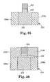
- Figure 36 illustrates a cross-sectional view of one embodiment of preprocessed wafer 220, bottom contact 232, storage location 204, and a dielectric material layer 210f.
- Dielectric material such as SiO 2 , SiO x , SiN, FSG, BPSG, BSG, low-k material, or other suitable dielectric material is deposited over exposed portions of preprocessed wafer 220, bottom contact 232, and storage location 204.
- the dielectric material is deposited using CVD, ALD, MOCVD, PVD, JVP, or other suitable deposition technique.
- the dielectric material is planarized using CMP or another suitable planarization technique to expose storage location 204 and provide dielectric material layer 210f.
- dielectric material layer 210f and insulation material 208a include the same material. In another embodiment, dielectric material layer 210f has a lower thermal conductivity than insulation material 208a. The process previously described with reference to Figures 9A-12 is then performed to fabricate second electrode 206 of phase change memory cell 280a as illustrated in Figure 34A or phase change memory cell 280b as illustrated in Figure 34B .
- Embodiments of the present invention provide a fabrication process for fabricating pillar type phase change memory cells.
- the phase change material storage location for each memory cell is fabricated using a first deposition, patterning, and etching process.
- the second electrode contacting the storage location is fabricated using a second deposition, patterning, and etching process. In this way, the structural integrity of the memory cell is maintained during the fabrication process.
Applications Claiming Priority (1)
| Application Number | Priority Date | Filing Date | Title |
|---|---|---|---|
| US11/643,438 US8017930B2 (en) | 2006-12-21 | 2006-12-21 | Pillar phase change memory cell |
Publications (2)
| Publication Number | Publication Date |
|---|---|
| EP1936710A2 true EP1936710A2 (de) | 2008-06-25 |
| EP1936710A3 EP1936710A3 (de) | 2010-04-21 |
Family
ID=39186107
Family Applications (1)
| Application Number | Title | Priority Date | Filing Date |
|---|---|---|---|
| EP07024825A Withdrawn EP1936710A3 (de) | 2006-12-21 | 2007-12-20 | Säulenförmige Phasenwechsel-Speicherzelle |
Country Status (5)
| Country | Link |
|---|---|
| US (1) | US8017930B2 (de) |
| EP (1) | EP1936710A3 (de) |
| JP (1) | JP2008235863A (de) |
| KR (1) | KR20080058271A (de) |
| CN (1) | CN101232075A (de) |
Families Citing this family (16)
| Publication number | Priority date | Publication date | Assignee | Title |
|---|---|---|---|---|
| US7989793B2 (en) * | 2007-12-10 | 2011-08-02 | Electronics And Telecommunications Research Institute | Electrical device using phase change material, phase change memory device using solid state reaction and method for fabricating the same |
| US7960203B2 (en) * | 2008-01-29 | 2011-06-14 | International Business Machines Corporation | Pore phase change material cell fabricated from recessed pillar |
| FR2934711B1 (fr) * | 2008-07-29 | 2011-03-11 | Commissariat Energie Atomique | Dispositif memoire et memoire cbram a fiablilite amelioree. |
| JP4635236B2 (ja) * | 2008-10-30 | 2011-02-23 | 独立行政法人産業技術総合研究所 | 固体メモリの製造方法 |
| JP4635235B2 (ja) * | 2008-10-30 | 2011-02-23 | 独立行政法人産業技術総合研究所 | 固体メモリ |
| JP2010183017A (ja) * | 2009-02-09 | 2010-08-19 | National Institute Of Advanced Industrial Science & Technology | 固体メモリ |
| JP2011023576A (ja) * | 2009-07-16 | 2011-02-03 | Hitachi Kokusai Electric Inc | 半導体装置の製造方法及び基板処理装置 |
| KR101333751B1 (ko) * | 2009-09-11 | 2013-11-28 | 도호쿠 다이가쿠 | 상변화 재료 및 상변화형 메모리 소자 |
| US8129268B2 (en) | 2009-11-16 | 2012-03-06 | International Business Machines Corporation | Self-aligned lower bottom electrode |
| US8233317B2 (en) * | 2009-11-16 | 2012-07-31 | International Business Machines Corporation | Phase change memory device suitable for high temperature operation |
| CN101931048A (zh) * | 2010-08-27 | 2010-12-29 | 复旦大学 | 一次可编程存储单元、存储器及其操作方法 |
| CN102005466A (zh) * | 2010-09-28 | 2011-04-06 | 中国科学院上海微系统与信息技术研究所 | 一种具有低k介质绝热材料的相变存储器结构及制备方法 |
| US20130306929A1 (en) * | 2012-05-16 | 2013-11-21 | Jaeho Lee | Multilayer-Stacked Phase Change Memory Cell |
| TWI549229B (zh) * | 2014-01-24 | 2016-09-11 | 旺宏電子股份有限公司 | 應用於系統單晶片之記憶體裝置內的多相變化材料 |
| JP6489480B2 (ja) * | 2014-06-12 | 2019-03-27 | パナソニックIpマネジメント株式会社 | 不揮発性記憶装置およびその製造方法 |
| US9564585B1 (en) | 2015-09-03 | 2017-02-07 | HGST Netherlands B.V. | Multi-level phase change device |
Citations (8)
| Publication number | Priority date | Publication date | Assignee | Title |
|---|---|---|---|---|
| US20050051901A1 (en) * | 2003-09-04 | 2005-03-10 | Bomy Chen | Memory device with discrete layers of phase change memory material |
| FR2861887A1 (fr) * | 2003-11-04 | 2005-05-06 | Commissariat Energie Atomique | Element de memoire a changement de phase a cyclabilite amelioree |
| US20060113573A1 (en) * | 2004-11-29 | 2006-06-01 | Byung-Ki Cheong | Phase change memory cell with transparent conducting oxide for electrode contact layer |
| US20060169968A1 (en) * | 2005-02-01 | 2006-08-03 | Thomas Happ | Pillar phase change memory cell |
| US20060175599A1 (en) * | 2005-02-10 | 2006-08-10 | Infineon Technologies North America Corp. | Phase change memory cell with high read margin at low power operation |
| EP1724850A2 (de) * | 2005-05-20 | 2006-11-22 | Infineon Technologies AG | Phasenwechselspeicherzelle mit geringem Leistungsverbrauch und großem Lesesignal |
| EP1732148A1 (de) * | 2005-06-07 | 2006-12-13 | Infineon Technologies AG | Phasenwechselspeicherzelle mit Ringkontakten |
| EP1923928A2 (de) * | 2006-11-17 | 2008-05-21 | Qimonda North America Corp. | Phasenwechselspeicherzelle mit Seitenwandkontakt |
Family Cites Families (6)
| Publication number | Priority date | Publication date | Assignee | Title |
|---|---|---|---|---|
| US7202171B2 (en) * | 2001-01-03 | 2007-04-10 | Micron Technology, Inc. | Method for forming a contact opening in a semiconductor device |
| US6507061B1 (en) * | 2001-08-31 | 2003-01-14 | Intel Corporation | Multiple layer phase-change memory |
| JP2005032855A (ja) * | 2003-07-09 | 2005-02-03 | Matsushita Electric Ind Co Ltd | 半導体記憶装置及びその製造方法 |
| US7361925B2 (en) * | 2005-02-10 | 2008-04-22 | Infineon Technologies Ag | Integrated circuit having a memory including a low-k dielectric material for thermal isolation |
| US20070045606A1 (en) * | 2005-08-30 | 2007-03-01 | Michele Magistretti | Shaping a phase change layer in a phase change memory cell |
| US7394088B2 (en) * | 2005-11-15 | 2008-07-01 | Macronix International Co., Ltd. | Thermally contained/insulated phase change memory device and method (combined) |
-
2006
- 2006-12-21 US US11/643,438 patent/US8017930B2/en not_active Expired - Fee Related
-
2007
- 2007-12-20 JP JP2007328265A patent/JP2008235863A/ja active Pending
- 2007-12-20 EP EP07024825A patent/EP1936710A3/de not_active Withdrawn
- 2007-12-21 KR KR1020070135388A patent/KR20080058271A/ko not_active Application Discontinuation
- 2007-12-21 CN CNA2007103015530A patent/CN101232075A/zh active Pending
Patent Citations (8)
| Publication number | Priority date | Publication date | Assignee | Title |
|---|---|---|---|---|
| US20050051901A1 (en) * | 2003-09-04 | 2005-03-10 | Bomy Chen | Memory device with discrete layers of phase change memory material |
| FR2861887A1 (fr) * | 2003-11-04 | 2005-05-06 | Commissariat Energie Atomique | Element de memoire a changement de phase a cyclabilite amelioree |
| US20060113573A1 (en) * | 2004-11-29 | 2006-06-01 | Byung-Ki Cheong | Phase change memory cell with transparent conducting oxide for electrode contact layer |
| US20060169968A1 (en) * | 2005-02-01 | 2006-08-03 | Thomas Happ | Pillar phase change memory cell |
| US20060175599A1 (en) * | 2005-02-10 | 2006-08-10 | Infineon Technologies North America Corp. | Phase change memory cell with high read margin at low power operation |
| EP1724850A2 (de) * | 2005-05-20 | 2006-11-22 | Infineon Technologies AG | Phasenwechselspeicherzelle mit geringem Leistungsverbrauch und großem Lesesignal |
| EP1732148A1 (de) * | 2005-06-07 | 2006-12-13 | Infineon Technologies AG | Phasenwechselspeicherzelle mit Ringkontakten |
| EP1923928A2 (de) * | 2006-11-17 | 2008-05-21 | Qimonda North America Corp. | Phasenwechselspeicherzelle mit Seitenwandkontakt |
Also Published As
| Publication number | Publication date |
|---|---|
| KR20080058271A (ko) | 2008-06-25 |
| US8017930B2 (en) | 2011-09-13 |
| US20080149909A1 (en) | 2008-06-26 |
| JP2008235863A (ja) | 2008-10-02 |
| CN101232075A (zh) | 2008-07-30 |
| EP1936710A3 (de) | 2010-04-21 |
Similar Documents
| Publication | Publication Date | Title |
|---|---|---|
| EP1936710A2 (de) | Säulenförmige Phasenwechsel-Speicherzelle | |
| US7688618B2 (en) | Integrated circuit having memory having a step-like programming characteristic | |
| US8084799B2 (en) | Integrated circuit with memory having a step-like programming characteristic | |
| US20070249090A1 (en) | Phase-change memory cell adapted to prevent over-etching or under-etching | |
| US7545668B2 (en) | Mushroom phase change memory having a multilayer electrode | |
| US7973301B2 (en) | Low power phase change memory cell with large read signal | |
| US20080265239A1 (en) | Integrated circuit including spacer material layer | |
| US7888665B2 (en) | Integrated circuit including memory cell having cup-shaped electrode interface | |
| EP1881539A2 (de) | Phasenwechsel-Speicherzelle mit stufenartiger Programmiereigenschaft | |
| US7541609B2 (en) | Phase change memory cell having a sidewall contact | |
| US7718464B2 (en) | Integrated circuit fabricated using an oxidized polysilicon mask | |
| EP1734593A2 (de) | Phasenwechselspeicherzelle definiert durch Stempellithographie | |
| US8189374B2 (en) | Memory device including an electrode having an outer portion with greater resistivity | |
| US20090003032A1 (en) | Integrated circuit including resistivity changing material having a planarized surface | |
| US20060273297A1 (en) | Phase change memory cell having ring contacts | |
| EP1848047A2 (de) | Übergang des Zustands von Phasenwechselmaterial durch Ausglühen | |
| US7679074B2 (en) | Integrated circuit having multilayer electrode | |
| US7696510B2 (en) | Integrated circuit including memory having reduced cross talk | |
| US20080272354A1 (en) | Phase change diode memory |
Legal Events
| Date | Code | Title | Description |
|---|---|---|---|
| PUAI | Public reference made under article 153(3) epc to a published international application that has entered the european phase |
Free format text: ORIGINAL CODE: 0009012 |
|
| AK | Designated contracting states |
Kind code of ref document: A2 Designated state(s): AT BE BG CH CY CZ DE DK EE ES FI FR GB GR HU IE IS IT LI LT LU LV MC MT NL PL PT RO SE SI SK TR |
|
| AX | Request for extension of the european patent |
Extension state: AL BA HR MK RS |
|
| PUAL | Search report despatched |
Free format text: ORIGINAL CODE: 0009013 |
|
| AK | Designated contracting states |
Kind code of ref document: A3 Designated state(s): AT BE BG CH CY CZ DE DK EE ES FI FR GB GR HU IE IS IT LI LT LU LV MC MT NL PL PT RO SE SI SK TR |
|
| AX | Request for extension of the european patent |
Extension state: AL BA HR MK RS |
|
| AKY | No designation fees paid | ||
| STAA | Information on the status of an ep patent application or granted ep patent |
Free format text: STATUS: THE APPLICATION IS DEEMED TO BE WITHDRAWN |
|
| 18D | Application deemed to be withdrawn |
Effective date: 20101022 |
|
| REG | Reference to a national code |
Ref country code: DE Ref legal event code: R108 Effective date: 20110405 Ref country code: DE Ref legal event code: 8566 |