EP1932939B1 - Beschichtungswerkstoff auf Basis einer Kupfer-Indium-Gallium-Legierung, insbesondere zur Herstellung von Sputtertargets, Rohrkathoden und dergleichen - Google Patents
Beschichtungswerkstoff auf Basis einer Kupfer-Indium-Gallium-Legierung, insbesondere zur Herstellung von Sputtertargets, Rohrkathoden und dergleichen Download PDFInfo
- Publication number
- EP1932939B1 EP1932939B1 EP07022072A EP07022072A EP1932939B1 EP 1932939 B1 EP1932939 B1 EP 1932939B1 EP 07022072 A EP07022072 A EP 07022072A EP 07022072 A EP07022072 A EP 07022072A EP 1932939 B1 EP1932939 B1 EP 1932939B1
- Authority
- EP
- European Patent Office
- Prior art keywords
- phase
- indium
- gallium
- copper
- coating material
- Prior art date
- Legal status (The legal status is an assumption and is not a legal conclusion. Google has not performed a legal analysis and makes no representation as to the accuracy of the status listed.)
- Not-in-force
Links
- 238000000576 coating method Methods 0.000 title claims abstract description 21
- APFVFJFRJDLVQX-UHFFFAOYSA-N indium atom Chemical compound [In] APFVFJFRJDLVQX-UHFFFAOYSA-N 0.000 title claims abstract description 20
- 239000000463 material Substances 0.000 title claims abstract description 18
- 239000011248 coating agent Substances 0.000 title claims abstract description 15
- 238000004519 manufacturing process Methods 0.000 title claims abstract description 13
- 239000010949 copper Substances 0.000 title abstract description 29
- 229910052802 copper Inorganic materials 0.000 title abstract description 13
- RYGMFSIKBFXOCR-UHFFFAOYSA-N Copper Chemical compound [Cu] RYGMFSIKBFXOCR-UHFFFAOYSA-N 0.000 title abstract description 7
- 229910000807 Ga alloy Inorganic materials 0.000 title description 4
- 229910000846 In alloy Inorganic materials 0.000 title 1
- 229910052738 indium Inorganic materials 0.000 claims abstract description 27
- 239000000203 mixture Substances 0.000 claims abstract description 24
- 229910052733 gallium Inorganic materials 0.000 claims abstract description 23
- 229910045601 alloy Inorganic materials 0.000 claims abstract description 21
- 239000000956 alloy Substances 0.000 claims abstract description 21
- GYHNNYVSQQEPJS-UHFFFAOYSA-N Gallium Chemical group [Ga] GYHNNYVSQQEPJS-UHFFFAOYSA-N 0.000 claims abstract description 14
- HCHKCACWOHOZIP-UHFFFAOYSA-N Zinc Chemical group [Zn] HCHKCACWOHOZIP-UHFFFAOYSA-N 0.000 claims abstract description 5
- 239000011159 matrix material Substances 0.000 claims description 9
- 239000011701 zinc Substances 0.000 claims description 5
- TVZPLCNGKSPOJA-UHFFFAOYSA-N copper zinc Chemical compound [Cu].[Zn] TVZPLCNGKSPOJA-UHFFFAOYSA-N 0.000 abstract 1
- 239000010410 layer Substances 0.000 description 22
- 238000000034 method Methods 0.000 description 14
- 238000002844 melting Methods 0.000 description 11
- 230000008018 melting Effects 0.000 description 10
- 238000000724 energy-dispersive X-ray spectrum Methods 0.000 description 9
- 238000004544 sputter deposition Methods 0.000 description 7
- 229910002056 binary alloy Inorganic materials 0.000 description 6
- 230000015572 biosynthetic process Effects 0.000 description 6
- 238000010348 incorporation Methods 0.000 description 6
- 229910052751 metal Inorganic materials 0.000 description 6
- 239000002184 metal Substances 0.000 description 6
- 239000000843 powder Substances 0.000 description 6
- 239000011669 selenium Substances 0.000 description 6
- 238000005477 sputtering target Methods 0.000 description 5
- 238000007740 vapor deposition Methods 0.000 description 5
- 150000001875 compounds Chemical class 0.000 description 4
- 238000002149 energy-dispersive X-ray emission spectroscopy Methods 0.000 description 4
- 230000008020 evaporation Effects 0.000 description 4
- 238000001704 evaporation Methods 0.000 description 4
- 238000005272 metallurgy Methods 0.000 description 4
- 238000005240 physical vapour deposition Methods 0.000 description 4
- BUGBHKTXTAQXES-UHFFFAOYSA-N Selenium Chemical compound [Se] BUGBHKTXTAQXES-UHFFFAOYSA-N 0.000 description 3
- 238000000137 annealing Methods 0.000 description 3
- 238000001816 cooling Methods 0.000 description 3
- 239000000155 melt Substances 0.000 description 3
- 229910052711 selenium Inorganic materials 0.000 description 3
- 239000004065 semiconductor Substances 0.000 description 3
- 238000001228 spectrum Methods 0.000 description 3
- 239000000758 substrate Substances 0.000 description 3
- 229910002058 ternary alloy Inorganic materials 0.000 description 3
- 238000002083 X-ray spectrum Methods 0.000 description 2
- 238000005266 casting Methods 0.000 description 2
- 238000000151 deposition Methods 0.000 description 2
- 230000008021 deposition Effects 0.000 description 2
- 238000010438 heat treatment Methods 0.000 description 2
- 238000011835 investigation Methods 0.000 description 2
- 238000001000 micrograph Methods 0.000 description 2
- 239000011148 porous material Substances 0.000 description 2
- 230000035939 shock Effects 0.000 description 2
- 239000000126 substance Substances 0.000 description 2
- 239000010409 thin film Substances 0.000 description 2
- 229910052725 zinc Inorganic materials 0.000 description 2
- 229910002535 CuZn Inorganic materials 0.000 description 1
- 240000002329 Inga feuillei Species 0.000 description 1
- ZOKXTWBITQBERF-UHFFFAOYSA-N Molybdenum Chemical compound [Mo] ZOKXTWBITQBERF-UHFFFAOYSA-N 0.000 description 1
- 238000002441 X-ray diffraction Methods 0.000 description 1
- 238000005275 alloying Methods 0.000 description 1
- 238000004458 analytical method Methods 0.000 description 1
- DVRDHUBQLOKMHZ-UHFFFAOYSA-N chalcopyrite Chemical group [S-2].[S-2].[Fe+2].[Cu+2] DVRDHUBQLOKMHZ-UHFFFAOYSA-N 0.000 description 1
- 238000010549 co-Evaporation Methods 0.000 description 1
- CDZGJSREWGPJMG-UHFFFAOYSA-N copper gallium Chemical compound [Cu].[Ga] CDZGJSREWGPJMG-UHFFFAOYSA-N 0.000 description 1
- HVMJUDPAXRRVQO-UHFFFAOYSA-N copper indium Chemical compound [Cu].[In] HVMJUDPAXRRVQO-UHFFFAOYSA-N 0.000 description 1
- 238000005336 cracking Methods 0.000 description 1
- 239000013078 crystal Substances 0.000 description 1
- 230000006735 deficit Effects 0.000 description 1
- 210000003298 dental enamel Anatomy 0.000 description 1
- 230000001419 dependent effect Effects 0.000 description 1
- 238000009826 distribution Methods 0.000 description 1
- 230000000694 effects Effects 0.000 description 1
- 238000009713 electroplating Methods 0.000 description 1
- 230000005496 eutectics Effects 0.000 description 1
- 230000004927 fusion Effects 0.000 description 1
- 239000011521 glass Substances 0.000 description 1
- 239000012535 impurity Substances 0.000 description 1
- 229910000765 intermetallic Inorganic materials 0.000 description 1
- 238000001755 magnetron sputter deposition Methods 0.000 description 1
- 238000010310 metallurgical process Methods 0.000 description 1
- 150000002739 metals Chemical class 0.000 description 1
- 229910052750 molybdenum Inorganic materials 0.000 description 1
- 239000011733 molybdenum Substances 0.000 description 1
- 238000000465 moulding Methods 0.000 description 1
- 238000003825 pressing Methods 0.000 description 1
- 230000001681 protective effect Effects 0.000 description 1
- 239000002994 raw material Substances 0.000 description 1
- 239000002356 single layer Substances 0.000 description 1
- 238000007711 solidification Methods 0.000 description 1
- 230000008023 solidification Effects 0.000 description 1
- 238000006467 substitution reaction Methods 0.000 description 1
Images


Classifications
-
- C—CHEMISTRY; METALLURGY
- C23—COATING METALLIC MATERIAL; COATING MATERIAL WITH METALLIC MATERIAL; CHEMICAL SURFACE TREATMENT; DIFFUSION TREATMENT OF METALLIC MATERIAL; COATING BY VACUUM EVAPORATION, BY SPUTTERING, BY ION IMPLANTATION OR BY CHEMICAL VAPOUR DEPOSITION, IN GENERAL; INHIBITING CORROSION OF METALLIC MATERIAL OR INCRUSTATION IN GENERAL
- C23C—COATING METALLIC MATERIAL; COATING MATERIAL WITH METALLIC MATERIAL; SURFACE TREATMENT OF METALLIC MATERIAL BY DIFFUSION INTO THE SURFACE, BY CHEMICAL CONVERSION OR SUBSTITUTION; COATING BY VACUUM EVAPORATION, BY SPUTTERING, BY ION IMPLANTATION OR BY CHEMICAL VAPOUR DEPOSITION, IN GENERAL
- C23C14/00—Coating by vacuum evaporation, by sputtering or by ion implantation of the coating forming material
- C23C14/22—Coating by vacuum evaporation, by sputtering or by ion implantation of the coating forming material characterised by the process of coating
- C23C14/34—Sputtering
- C23C14/3407—Cathode assembly for sputtering apparatus, e.g. Target
- C23C14/3414—Metallurgical or chemical aspects of target preparation, e.g. casting, powder metallurgy
Definitions
- the most common method of producing the CIGS layer on an industrial scale is the co-sputtering of targets consisting of CuGa (65). 80% by weight of Cu) and In.
- targets consisting of CuGa (65). 80% by weight of Cu) and In.
- the selenization is carried out in a subsequent annealing step at 500 ° C in a Se-containing atmosphere (duration about 3 minutes).
- the ⁇ -phase can be defined as a cubic phase system.
- a cubic phase of the Cu5Zn8 prototype phase lattice is established at a defined alloy composition, melt flow and solidification rate, in which case gallium takes the place of zinc.
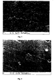
- Fig. 1 shows the micrograph of the alloy CuInGa 35.8 - 52.4 - 11.8wt%, cooled quickly.
- the ⁇ phase are the dark areas surrounded by an indium matrix.
- Fig. 3 shows an X - ray spectrum of the ⁇ phase.
Landscapes
- Chemical & Material Sciences (AREA)
- Chemical Kinetics & Catalysis (AREA)
- Engineering & Computer Science (AREA)
- Materials Engineering (AREA)
- Mechanical Engineering (AREA)
- Metallurgy (AREA)
- Organic Chemistry (AREA)
- Physical Vapour Deposition (AREA)
Description
- Die Erfindung betrifft einen Beschichtungswerkstoff auf Basis einer Kupfer-Indium-Gallium(CuInGa)-Legierung insbesondere zur Herstellung von Sputtertargets, Rohrkathoden und dergleichen Beschichtungswerkstoffquellen.
- Die schmelzmetallurgische Herstellung einer CuInGa-Legierung ist grundsätzlich aus der
DE 698 35 851 T2 bekannt. Die dort erwähnte Legierung entspricht in ihren Anteilsverhältnissen im Wesentlichen denen der im Folgenden offenbarten Erfindung. DieEP 0 308 201 A1 bezieht sich auf ein Sputtertarget zur Verwendung im Produktionsprozess von magnetooptischen Aufzeichnungsmedien. Entsprechend offenbartUS 6 682 636 B2 PVD-Targets und Verfahren zu ihrer Bildung. Beide Druckschriften lehren jedoch nicht die Verwendung einer CuInGa-Legierung als Beschichtungswerkstoff. Nächstliegender Stand der Technik ist dieEP 0 881 695 A2 , die ein Pulver, bestehend aus 50,78 Gew.-% Indium, 36 Gew.-% Kupfer und 13,22 Gew.-% Ga. Dieses Pulver wird nach der Beimischung von Selen zur Herstellung einer Schicht verwendet. - Einsatzgebiet ist die Herstellung von Dünnschichtsolarzellen mit einer Halbleiterschicht aus CuInGaSe2 oder CuInGaS2 (Sammelabkürzung: CIGS). Hierbei wird eine elektrisch leitfähige CuInGa - Schicht in gewünschter Zusammensetzung auf ein mit Molybdän beschichtetes Substrat (KNS-Glas) abgeschieden, z.B. aufgedampft oder gesputtert. In einem weiterführenden Schritt wird die Schicht in Se- oder S-haltiger Atmosphäre selenisiert oder sulfitisiert, um ihre halbleitenden Eigenschaften zu erhalten. Die CIGS - Schicht ist ein Teil der aus einem Schichtpaket aufgebauten Schichtsystem einer Dünnschichtsolarzelle.
- Das Aufbringen der CuInGa Schicht erfolgt bisher über Koverdampfen elementarer Verdampfungsquellen (Cu, In, Ga separat) oder über schichtweise abwechselndes Aufdampfen binärer Vorlegierungen aus dem System Cu - In - Ga. Diese Prozesse können nur schwer über einen längeren Zeitraum konstante Ergebnisse in der Schichtzusammensetzung liefern. Ein Problem ist z.B. ein Cu - Defizit beim Einsatz dieser Methoden oder eine Ungleichverteilung der eingesetzten Elemente.
- Zudem sind oft mehrere Schritte zum Aufbringen der CIG - Schicht notwendig, da nicht alle drei Elemente durch Sputtern abgeschieden werden können. Ga nämlich besitzt einen Schmelzpunkt von 30°C, was während dem Beschichtungsprozess unweigerlich zum Aufschmelzen und somit Abtropfen des Ga-Metalls führt.
- Die elektrische Leitfähigkeit aufgrund der Halbleitereigenschaften dieses Metalls ist sehr schlecht. Dieses wiederum führt zur Erhitzung des Gallium-Metalls bis zur schmelzflüssigen Phase. Der Beschichtungsprozess kommt somit zum Erliegen.
- Nach jetzigem Kenntnisstand werden bereits Sputtertargets, planar oder als Rohrkathoden, mit den drei Komponenten Cu, In und Ga zum Erzeugen der halbleitenden CIGS - Schichten entwickelt, zeigen jedoch vielfältige ungünstige Materialerscheinungen sowie durch ungeeignete Schmelzführung bei der Herstellung des ternären Beschichtungswerkstoffs sehr schlechte Sputter- und Schichteigenschaften.
- Bisherige Verfahren zur Herstellung der CIGS - Schicht auf verschiedenen Substraten sind folgende:
- Bei simultanem Aufdampfen der einzelnen Elemente mit verschiedenen Aufdampfraten mit und ohne Selen mit nachfolgendem Temperschritt reagiert die Schicht zur halbleitenden Chalkophyrit-Struktur.
- Aufdampfen (Ga)/Aufsputtern (In/Cu) als einzelne Schichten mit nachfolgendem Temperschritt (mit Selenisierung) - dies auch unter Verwendung binärer Metalltargets (CuGa + In oder CuIn + Ga) verschiedener Zusammensetzungen.
- Aufsputtern der Oxidverbindungen der drei Metalle mit nachfolgender Reduzierung in z.B. H2 zur reinen Metallschicht.
- Schichtabscheidung ausgehend von den Se - haltigen Verbindungen In2Se3, Ga2Se3, In/Ga2Se3 und Cu2Se.
- Magnetronsputtern der direkten Verbindungshalbleitermaterialien Cu-InSe2 oder CuInS2. Die damit hergestellten Solarzellen weisen einen zu geringen Wirkungsgrad auf.
- Weitere Verfahren, die sich mit dem galvanischen Aufbringen oder Aufdrucken der einzelnen Schichten beschäftigen, befinden sich in der Testphase.
- In keinem der oben genannten "herkömmlichen" Herstellungsverfahren wurde ein Sputtertarget erfolgreich verwendet, das die drei Elemente Cu, In und Ga im gewünschten Verhältnis in sich vereinigt.
- Die gängigste Methode zur Herstellung der CIGS - Schicht im industriellen Maßstab ist das Ko - Sputtern von Targets bestehend aus CuGa (65 - 80 Gew.% Cu) und In. Die Selenisierung erfolgt in einem nachfolgenden Temperschritt bei 500°C in Se-haltiger Atmosphäre (Dauer ca. 3min).
- Die Vorteile der entwickelten CuInGa - Targets in den gewünschten Zusammensetzungen liegen in der Verwendung eines einzigen Sputtertarget für den Beschichtungsprozess. Dies bietet höhere Prozessstabilität und genau einstellbare Stöchiometrien sowie Kostenreduzierung und Recyclingfähigkeit der Rest-Beschichtungsmaterialien sowie eine notwendig hohe Schmelztemperatur der Legierung besonders bezüglich des Elements Gallium.
- Aufgabe der vorliegenden Erfindung ist es, einen Beschichtungswerkstoff bereitzustellen, mit dem ein Aufdampfen von CIG-Schichten in einem einzigen Schritt möglich ist. Mit einer Verdampfungsquelle, die die richtige Zusammensetzung, eine gute elektrische Leitfähigkeit besitzt und deren Schmelzpunkt über 200°C liegt, wird der Prozess nämlich auf einen PVD-Beschichtungsschritt verkürzt. Die gewünschte Zusammensetzung der Schicht ist dann kein Problem mehr, die Selenierung kann wie gehabt nachfolgend durch Verdampfung erfolgen.
- Diese Aufgabe wird durch die im Patentanspruch 1 angegebenen Legierungsmerkmale gelöst.
- Demnach weist die als Beschichtungswerkstoff zum Einsatz kommende Kupfer-Indium-Gallium-Legierung eine Phase nach Art einer Prototyp-Cu5Zn8-Phase auf, in der die Gitterplätze der Zinkatome (Zn) durch Galliumatome besetzt sind (Gallium-substituierte Cu5Zn8-Phase) und bei der zugleich Indium mit einem Anteil von bis zu 26 Gew.% in die Elementarzelle oder Phase eingelagert ist zugleich Indium mit einem Anteil von bis zu 22 Gew.% in die Elementarzelle oder Phase eingelagert ist
- Vorzugsweise ist die Verwendbarkeit dieser ternären Legierung für den Beschichtungsprozess gewährleistet.
- Das Herstellungsverfahren für den erfindungsgemäßen Beschichtungswerkstoff weist folgenden Verfahrensschritt auf:
- Die Legierung wird schmelzmetallurgisch aus den Bestandteilen Cu, In und Ga hergestellt.
- Eine bevorzugte Ausführungsform der Erfindung ist im abhängigen Ansprüch 2 angegeben.
- Grundsätzlich ist es auch möglich, dass sich ausgehend von pulvermetallurgischen Herstellungsprozessen der ternären Zusammensetzung erst während des Beschichtungsverfahrens "in statu nascendi" eine Gallium-substituierte Cu5Zn8-Phase mit Einlagerung von Indium bildet. So können pulvermetallurgische Verfahren verwendet werden, um CuInGa-Materialien herzustellen, die entweder aus Elementpulvern oder Legierungspulvern der binären Legierungen hergestellt werden. Die Pulver werden entsprechend der gewünschten Endzusammensetzung gemischt und durch Pressen entsprechender Formteile hergestellt. Die Ausbildung der notwendigen Phase kann bei diesen Materialien auf der Targetoberfläche oder sogar erst auf dem Substrat selber als dünne Schicht erfolgen.
- Hinsichtlich der Kupfer-Indium-Gallium-Legierung hat sich überraschenderweise gezeigt, dass bei definierter Legierungszusammensetzung des sogar bis zu > 400 °C erhöht werden kann, ohne dass eine selektives Aufschmelzen der Elemente Ga und In erfolgt, obwohl die Schmelztemperaturen dieser Elemente mit Ga = 30 °C und In = 156 °C weit darunter liegen.
- Eingehende Phasenuntersuchungen haben gezeigt, dass durch die angestrebte Bildung von intermetallischen Verbindungen mit gleichzeitiger Einlagerung eines weiteren dritten Elements in den Tetraeder- oder Oktaederlücken dieser Phase der gewünschte Effekt der Schmelztemperaturerhöhung erzielt werden kann. Begründet wird dies durch die in dieser Phase sich einstellenden Bindungsenergien, die die Summe aus metallischen und kovalenten Bindungsanteilen ermöglichen. Notwendiges "Muss" bleibt hierbei die Möglichkeit der Einlagerung eines dritten Elements in Volumenanteilen von mindestens bis zu 22 Gew.%.
- Die Phasenbildung mit einhergehender Einlagerung war bis dato im ternären System Cu - In - Ga unbekannt und ist in diesem Fall von der sich durch die genauen Legierungszusammensetzung, den Herstellungsparametem und der verwendeten Schmelztechnik abhängig.
- Weitere Untersuchungen haben gezeigt, dass diese neu entdeckte Phase aufgrund der geometrischen Anforderung der Atome Cu und Gallium ähnlich der bekannten Prototyp-Phase Cu5Zn8 ist, wobei in diesem speziellen Fall die Zn-Atome durch Ga ersetzt werden. Bemerkenswert ist hierbei der Einbau von In-Atomen mit einem Anteil von bis zu > 22 Gew.% Indium in die Phase. Erst durch die Bildung dieser Phase wird somit die Verwendbarkeit des Beschichtungswerkstoffs sichergestellt. Hierbei ist ebenfalls wichtig, dass diese bisher nicht in der Literatur bekannte Phase die Verdampfungs- und Sputtereigenschaften dieser ternären Legierung in keinem Fall negativ beeinflussen. Der Nachweis hierfür wurde in mehreren Beschichtungsversuchen sichergestellt.
- Die π -Phase definiert sich somit im ternären Cu - In - Ga-Legierungssystem als Phase des Prototyp-Gittertyps - Cu5Zn8 mit gleichzeitiger Einlagerung von bis zu >22 Gew.% an Indium, wobei das Indium röntgendiffraktometrisch ungeordnet in den vorhandenen Tetraeder- und Oktraederlücken der Elementarzelle der Phase eingelagert ist.
- In Anlehnung an den Phasen-Prototyp Cu5Zn8 ergeben sich folgende Literaturwerte:
Temperatur (k) Dichte 8,054 g/cm3 Molares Volumen 1.04402 cm3/mol Expansionskoeffizient 26,90 (10-6/k) Spez. Wärme 387 (J/kg k) Atom-Positionen X = 0,313 Y = 0,313 Z = 0,036 Volumengruppe 143m - Somit lässt sich die π -Phase als kubisches Phasensystem definieren.
- Im Folgenden wird die Erfindung anhand der beigefügten Zeichnungen näher beschrieben. Es zeigen:
- Fig. 1
- ein Anschliffbild einer Legierung CuInGa 35,8 - 52,4 - 11,8wt%, schnell abgekühlt,
- Fig. 2
- ein Anschliffbild einer Legierung CuInGa 62 - 17 - 21 wt%, π - Phase - mit verfahrentechnisch bedingten Gussporen,
- Fig. 3
- ein Röntgenspektrum der π - Phase,
- Fig. 4
- ein EDX - Spektrum zur Bestimmung der chem. Zusammensetzung der in
Fig. 1 zu sehenden dunklen Bereiche (π - Phase), - Fig. 5
- ein EDX - Spektrum der hellen Matrix aus
Fig.1 , - Fig. 6
- ein Anschliffbild mit π - Phase bei langsamerer Abkühlung,
- Fig. 7
- ein EDX-Spektrum der π - Phase der langsam abgekühlten Schmelze,
- Fig. 8
- ein EDX-Spektrum der Matrix der langsam abgekühlten Schmelze, und
- Fig. 9
- EDX - Spektren von sechs untersuchten Punkten auf der Schlifffläche von
Fig. 2 . - Innerhalb erschmolzener CuInGa - Legierungen stellt sich bei definierter Legierungszusammensetzung und Schmelzenführung sowie Erstarrungsgeschwindigkeit eine kubische Phase des Prototypen-Phasen-Gittertyps Cu5Zn8 ein, wobei in diesem Fall Gallium den Platz des Zink einnimmt.
- Indium ist bis zu 22 Gewichtsprozent (wt%) in dieser Phase gelöst. Indium-Gehalte größer 25wt% scheiden sich als die o.g. Phase umgebende Matrix aus. Bei Kupfer-Gehalten über 63wt% werden Indium und Gallium entweder im Cu gelöst oder bilden mit Kupfer folgende binäre Verbindungen:
Phase Stabilitätsbereich in K Cu2Ga γ1 298-918 Cu2Ga γ 763-1109 Cu3Ga β 298-1188 Cu5Ga3 γ2 298-758 Cu7Ga2 ζ' 298-595 Cu7Ga2 ζ 603-893 Cu7In4 δ 298-904 Cu4In β 847-983 - Das binäre Legierungssystem InGa bildet keine Phasen, dafür ein niedrigschmelzendes Eutektikum bei 15 °C aus.
- Dies ist entnehmbar folgender Literatur:
- "Constitution Of Binary Alloys", Hansen, 2. Auflage 1958 ; Metallurgy and Metallurgical Engineering Series.
- TAPP Plus Version 2.2; E S Microwave Inc.
- Bedingt durch die Bildung der Phase hier des Phasen-Prototyps Cu5Zn8 mit Substitution von Zink durch Gallium mit gleichzeitiger Einlagerung von Indium (im folgenden π - Phase genannt) wird die geringe Schmelztemperatur der Elemente Gallium von 302,91K auf Temperaturen weit größer 502,91K und Indium von 429,15K auf größer 529,15K erhöht. Dies bedingt, dass somit das von nicht legierten ternären Legierungen bekannte frühe Aufschmelzen besonders von Gallium verhindert wird und somit die Legierung für PVD - Beschichtungsprozesse, besonders beim Sputterprozess oder anderen PVD-Prozessen, eingesetzt werden kann. Die bekannten binären Legierungen aus Kupfer-Gallium und Kupfer-Indium im Verhältnis der π - Phase zeigen eine derartige Sprödigkeit, dass diese nicht oder nur sehr schwer mechanisch bearbeitet werden können. Auch die notwendige Thermoschockbeständigkeit ist bei den binären Legierungen nicht gegeben, so dass diese binären Legierungen nicht oder nur sehr eingeschränkt Verwendung finden.
- Die Zusammensetzung der Phase wurde an einem Rasterelektronenmikroskop mit EDX - Analyse statistisch ermittelt. Als Proben dienten drei metallographische Anschliffe verschiedener chemischer Zusammensetzungen aus dem System CuInGa. In jeder Probe war die charakteristische π - Phase zu finden. In jedem Anschliff wurde die Zusammensetzung an 10 Punkten untersucht, die augenscheinlich zur π - Phase gehörten.
- Die π - Phase entspricht demnach folgender Zusammensetzung:
- CuInGa: 59 - 63 : 9-22 : 19 - 28 wt%
-
Fig. 1 zeigt die Anschliffbild der Legierung CuInGa 35,8 - 52,4 - 11,8wt%, schnell abgekühlt. Die π - Phase sind die dunklen Bereiche, die von einer Indium-Matrix umgeben sind. - Eine Röntgenphasenanalyse wurde durchgeführt.
- Ausgehend von den obigen Daten wurde eine Schmelze mit einer Durchschnittszusammensetzung CuInGa 62:17:21wt% hergestellt und der Phasenbestand mittels Röntgendiffraktometrie bestimmt.
-
Fig. 2 zeigt ein Anschliffbild der Legierung CuInGa 62 - 17 - 21 wt%, π - Phase - mit verfahrentechnisch bedingten Gussporen. -
Fig 3 zeigt ein Röntgenspektrum der π - Phase. - Zwei charakteristische Peaks des Spektrums liegen bei 2 Theta - Winkeln von 37,9° und 48° und stimmen mit dem Hauptpeak der Prototyp-Phase Cu5Zn8 überein. Auch die weiteren Reflexe der Prototyp-Cu5Zn8-Phase (braune Linien ) stimmen mit dem vorliegenden Spektrum der π - Phase überein.
- Neben der Prototyp-Cu5Zn8 - Phase zeigt das Spektrum noch elementares Kupfer (grau) und Gallium (grün) an sowie eine weitere Phase CuZn (hellblau), wobei die Prototyp-Phase Cu5Zn8 am stärksten mit der vorliegenden π - Phase übereinstimmt. Die Reflexe kommen durch die Gitterebenenabstände der in der Probe vorliegenden Phasen zustande.
- Die elektrische Leitfähigkeit wurde bestimmt. Gemessen wurde der Durchgangswiderstand durch mehrere Achsen einer CuInGa - Scheibe mit den in
Fig. 1 und 2 abgebildeten Zusammensetzungen. Der Widerstand lag dabei unterhalb des Messbereich des Multimeters, der bei ca. 300 mΩ liegt. Das Material ist damit sehr gut elektrisch leitfähig. - Die Herstellung erfolgt schmelzmetallurgisch unter Schutzgasatmosphäre bei einem Druck von 100 - 600mbar. Bei kleinerem Druck verdampft zu viel In und Ga. Die Schmelze erfolgt in einem Tiegel mit den Eigenschaften:
- ➢ Wärmeleitfähigkeit < 80 W/mK
- ➢ Elektische Leitfähigkeit > 0,05 MS/m
- ➢ Chemische Resistenz gegenüber der Schmelze.
- ➢ Temperaturschockbeständigkeit.
- ➢ Indirekt gekühlt
- Die Abkühlgeschwindigkeit wird so eingestellt, dass die Kristallgröße 10 µm nicht übersteigt. Der Energieeintrag kann induktiv, über Lichtbogen oder Heizelemente usw. erfolgen. Als Rohstoffe dienen die Elemente Cu, In und Ga sowie jegliche binären oder ternären Vorlegierungen dieses Dreistoffsystems.
-
Fig. 4 zeigt ein EDX - Spektrum zur Bestimmung der chem. Zusammensetzung der inFig. 1 zu sehenden dunklen Bereiche (π - Phase). -
Fig. 5 zeigt ein EDX - Spektrum der hellen Matrix ausFig.1 , das fast nur Indium anzeigt. Kupfer und Gallium sind nur noch im Maßstab von Verunreinigungen enthalten. -
Fig. 6 zeigt die π - Phase, die bei langsamerer Abkühlung größere Körner ausbildet und rissempfindlich wird. -
Fig. 7 zeigt die π - Phase der langsam abgekühlten Schmelze und weist ein gleiches EDX - Spektrum auf wie inFig. 2 . -
Fig. 8 zeigt, dass die Matrix der langsam abgekühlten Schmelz wiederum fast ausschließlich aus Indium besteht. - Die EDX - Spektren gemäß
Fig. 9 von sechs untersuchten Punkten auf der Schlifffläche vonFig. 2 zeigen deren Zusammensetzungen. Alle Punkte haben in etwa die selbe Zusammensetzung.
Claims (2)
- Beschichtungswerkstoff, insbesondere zur Herstellung von Sputtertargets, Rohrkathoden und dergleichen, aus einer Kupfer-Indium-Gallium(CuInGa-)Legierung, umfassend eine Indium-Matrix, in der eine Phase nach Art einer Prototyp-Cu5Zn8-Phase, in der die Gitterplätze der Zinkatome (Zn) durch Galliumatome besetzt sind (Gallium-substituierte Cu5Zn8-Phase), ausgebildet ist und bei welcher Gallium-substituierten Cu5Zn8-Phase zugleich Indium mit einem Anteil von bis zu 22 Gew.% in die Elementarzelle oder Phase eingelagert ist,
dadurch gekennzeichnet, dass die Gallium-substituierte Cu5Zn8-Phase eine Zusammensetzung mit den Anteilsbereichen Cu:In:Ga von 59-63 : 9 - 22 : 19 - 28 Gew.-% aufweist. - Beschichtungswerkstoff nach Anspruch 1, gekennzeichnet durch eine Zusammensetzung von 34 - 38 Gew.-% Cu, 50 - 54 Gew.-% In und 10 - 13 Gew.-% Ga, vorzugsweise 35,8 - 52,4 - 11,8 Gew.-%.
Priority Applications (1)
| Application Number | Priority Date | Filing Date | Title |
|---|---|---|---|
| SI200730808T SI1932939T1 (sl) | 2006-11-23 | 2007-11-14 | Prevlečni material na osnovi zlitine baker-indij-galij, zlasti za izdelavo tarč za naprševanje cevnih katod in podobnega |
Applications Claiming Priority (1)
| Application Number | Priority Date | Filing Date | Title |
|---|---|---|---|
| DE102006055662A DE102006055662B3 (de) | 2006-11-23 | 2006-11-23 | Beschichtungswerkstoff auf Basis einer Kupfer-Indium-Gallium-Legierung, insbesondere zur Herstellung von Sputtertargets, Rohrkathoden und dergleichen |
Publications (2)
| Publication Number | Publication Date |
|---|---|
| EP1932939A1 EP1932939A1 (de) | 2008-06-18 |
| EP1932939B1 true EP1932939B1 (de) | 2011-10-26 |
Family
ID=38976154
Family Applications (1)
| Application Number | Title | Priority Date | Filing Date |
|---|---|---|---|
| EP07022072A Not-in-force EP1932939B1 (de) | 2006-11-23 | 2007-11-14 | Beschichtungswerkstoff auf Basis einer Kupfer-Indium-Gallium-Legierung, insbesondere zur Herstellung von Sputtertargets, Rohrkathoden und dergleichen |
Country Status (9)
| Country | Link |
|---|---|
| US (1) | US7717987B2 (de) |
| EP (1) | EP1932939B1 (de) |
| CN (1) | CN101195904B (de) |
| AT (1) | ATE530678T1 (de) |
| DE (1) | DE102006055662B3 (de) |
| DK (1) | DK1932939T3 (de) |
| ES (1) | ES2372622T3 (de) |
| PT (1) | PT1932939E (de) |
| SI (1) | SI1932939T1 (de) |
Families Citing this family (17)
| Publication number | Priority date | Publication date | Assignee | Title |
|---|---|---|---|---|
| US8467297B2 (en) * | 2005-03-10 | 2013-06-18 | Thomson Licensing | Hybrid mesh routing protocol |
| BRPI0520670B1 (pt) * | 2005-11-09 | 2018-11-27 | Thomson Licensing | seleção de rota em redes sem fio |
| US20100108503A1 (en) * | 2008-10-31 | 2010-05-06 | Applied Quantum Technology, Llc | Chalcogenide alloy sputter targets for photovoltaic applications and methods of manufacturing the same |
| DE102009015638A1 (de) * | 2009-03-24 | 2010-09-30 | Wieland Dental + Technik Gmbh & Co. Kg | Rohrförmiges Sputtertarget und Verfahren zu seiner Herstellung |
| JP5643524B2 (ja) * | 2009-04-14 | 2014-12-17 | 株式会社コベルコ科研 | Cu−Ga合金スパッタリングターゲットおよびその製造方法 |
| KR101067337B1 (ko) * | 2009-08-20 | 2011-09-23 | 연세대학교 산학협력단 | 물리적 증착용 타겟 제조 방법 |
| US20110089030A1 (en) * | 2009-10-20 | 2011-04-21 | Miasole | CIG sputtering target and methods of making and using thereof |
| US8709335B1 (en) | 2009-10-20 | 2014-04-29 | Hanergy Holding Group Ltd. | Method of making a CIG target by cold spraying |
| US8709548B1 (en) * | 2009-10-20 | 2014-04-29 | Hanergy Holding Group Ltd. | Method of making a CIG target by spray forming |
| US8342229B1 (en) | 2009-10-20 | 2013-01-01 | Miasole | Method of making a CIG target by die casting |
| CN102893370B (zh) * | 2010-03-17 | 2015-12-16 | 陶氏环球技术有限责任公司 | 整合连接层的光电活性的、基于硫属元素的薄膜结构 |
| WO2012074609A1 (en) | 2010-11-30 | 2012-06-07 | Dow Global Technologies Llc | Refurbishing copper and indium containing alloy sputter targets |
| US9150958B1 (en) | 2011-01-26 | 2015-10-06 | Apollo Precision Fujian Limited | Apparatus and method of forming a sputtering target |
| DE102011012034A1 (de) * | 2011-02-22 | 2012-08-23 | Heraeus Materials Technology Gmbh & Co. Kg | Rohrförmiges Sputtertarget |
| US8871143B2 (en) * | 2012-01-20 | 2014-10-28 | Leonard Nanis | Amalgam method for forming a sputter target useful in the manufacture of thin-film solar photovoltaic cells |
| AT13564U1 (de) * | 2013-01-31 | 2014-03-15 | Plansee Se | CU-GA-IN-NA Target |
| US9916958B1 (en) | 2014-01-30 | 2018-03-13 | Radiation Monitoring Devices, Inc. | Alkali semi-metal films and method and apparatus for fabricating them |
Family Cites Families (8)
| Publication number | Priority date | Publication date | Assignee | Title |
|---|---|---|---|---|
| DE3885690T2 (de) * | 1987-09-17 | 1994-06-09 | Seiko Epson Corp | Verfahren zum Herstellen eines Zerstäubungstargets zur Verwendung bei der Herstellung eines magnetooptischen Aufzeichnungsmediums. |
| US5985691A (en) | 1997-05-16 | 1999-11-16 | International Solar Electric Technology, Inc. | Method of making compound semiconductor films and making related electronic devices |
| US6682636B2 (en) * | 2000-08-18 | 2004-01-27 | Honeywell International Inc. | Physical vapor deposition targets and methods of formation |
| AU2003275239A1 (en) * | 2002-09-30 | 2004-04-23 | Miasole | Manufacturing apparatus and method for large-scale production of thin-film solar cells |
| DE202004021800U1 (de) * | 2003-08-14 | 2011-04-21 | University Of Johannesburg | Halbleiterfilme aus einer quartären oder höheren Legierung der Gruppe I-III-VI |
| CN1257560C (zh) * | 2003-12-05 | 2006-05-24 | 南开大学 | 铜铟镓的硒或硫化物半导体薄膜材料的制备方法 |
| US7605328B2 (en) * | 2004-02-19 | 2009-10-20 | Nanosolar, Inc. | Photovoltaic thin-film cell produced from metallic blend using high-temperature printing |
| CN100413097C (zh) * | 2005-06-03 | 2008-08-20 | 清华大学 | 铜铟镓硒或铜铟镓硫或铜铟镓硒硫薄膜太阳能电池吸收层的制备方法 |
-
2006
- 2006-11-23 DE DE102006055662A patent/DE102006055662B3/de not_active Expired - Fee Related
-
2007
- 2007-11-14 ES ES07022072T patent/ES2372622T3/es active Active
- 2007-11-14 PT PT07022072T patent/PT1932939E/pt unknown
- 2007-11-14 EP EP07022072A patent/EP1932939B1/de not_active Not-in-force
- 2007-11-14 AT AT07022072T patent/ATE530678T1/de active
- 2007-11-14 DK DK07022072.8T patent/DK1932939T3/da active
- 2007-11-14 SI SI200730808T patent/SI1932939T1/sl unknown
- 2007-11-20 US US11/943,003 patent/US7717987B2/en not_active Expired - Fee Related
- 2007-11-23 CN CN2007101596125A patent/CN101195904B/zh not_active Expired - Fee Related
Also Published As
| Publication number | Publication date |
|---|---|
| EP1932939A1 (de) | 2008-06-18 |
| ES2372622T3 (es) | 2012-01-24 |
| CN101195904B (zh) | 2010-06-09 |
| CN101195904A (zh) | 2008-06-11 |
| US20080121137A1 (en) | 2008-05-29 |
| DE102006055662B3 (de) | 2008-06-26 |
| SI1932939T1 (sl) | 2012-02-29 |
| PT1932939E (pt) | 2011-12-20 |
| DK1932939T3 (da) | 2012-02-13 |
| US7717987B2 (en) | 2010-05-18 |
| ATE530678T1 (de) | 2011-11-15 |
Similar Documents
| Publication | Publication Date | Title |
|---|---|---|
| EP1932939A1 (de) | Beschichtungswerkstoff auf Basis einer Kupfer-Indium-Gallium-Legierung, insbesondere zur Herstellung von Sputtertargets, Rohrkathoden und dergleichen | |
| DE69308465T2 (de) | Verfahren zur Herstellung einer dünnen Schicht aus einer Zusammensetzung des Typs Chalcopyrit | |
| DE69835851T2 (de) | Verfahren zur Herstellung von dünnen Schichten aus Gruppe IB-IIIA-VIA Verbindungshalbleitern und Verfahren zur Herstellung eines photovoltäischen Bauelements | |
| TWI458847B (zh) | Cu-Ga alloy sintered body sputtering target, a method for manufacturing the target, a light absorbing layer made of a Cu-Ga alloy sintered body target, and a CIGS solar cell using the light absorbing layer | |
| DE69304143T2 (de) | Methode zur Herstellung einer Zusammensetzung des Typs Chalkopyrit | |
| US9103000B2 (en) | Low melting point sputter targets for chalcogenide photovoltaic applications and methods of manufacturing the same | |
| KR20110084435A (ko) | 광전지 적용을 위한 칼코겐화물 합금 스퍼터 타깃 및 그 제조 방법 | |
| AT7491U1 (de) | Werkstoff für leitbahnen aus kupferlegierung | |
| EP2684212A1 (de) | Verfahren zur herstellung des pentanären verbindungshalbleiters cztsse, sowie dünnschichtsolarzelle | |
| EP2951332B1 (de) | Sputtertarget mit Ga-Na, In-Na oder Ga-In-Na intermetallischen Phasen | |
| DE3003285C2 (de) | ||
| EP3168325A1 (de) | Sputtertarget auf der basis einer silberlegierung | |
| EP0337007B1 (de) | Hartstoff-Schutzschicht mit homogener Elementverteilung | |
| WO2005064046A1 (de) | Verfahren zur herstellung von cu(in,ga)se2 einkritstallinem pulver und monokornmembran-solarzelle enthaltend dieses pulver | |
| DE19721649A1 (de) | Verfahren zur Herstellung eines Mischkristallpulvers mit geringem elektrischem Widerstand | |
| DE69017556T2 (de) | Thermoelektrisches Fe-Silizid-Konversionsmaterial vom P-Typ. | |
| DE102014225862B4 (de) | Verfahren zur Bildung einer Dünnschicht mit Gradient mittels Spraypyrolyse | |
| DE2361984C2 (de) | Anordnung und Verfahren zum Abscheiden amorpher Halbleiter-Dünnfilme sowie Verfahren zur Herstellung der benötigten Sublimationsquellen | |
| DE4447244A1 (de) | Widerstandsschicht | |
| WO2024165268A1 (de) | Siliziumhaltige übergangsmetallboridverdampfungsquelle | |
| WO2015042622A1 (de) | Kupfer-gallium sputtering target | |
| Bernede et al. | Optimization of a MoSe2 thin film deposition technique | |
| DE10248927B4 (de) | Dünnschichtsolarzelle mit elektrischer Molybdän-Kontaktschicht und Herstellungsverfahren | |
| WO2004075212A1 (de) | Pvd-beschichtungsmaterial | |
| DE10392993B4 (de) | Thermoelektrisches Material enthaltend Stickstoff |
Legal Events
| Date | Code | Title | Description |
|---|---|---|---|
| PUAI | Public reference made under article 153(3) epc to a published international application that has entered the european phase |
Free format text: ORIGINAL CODE: 0009012 |
|
| AK | Designated contracting states |
Kind code of ref document: A1 Designated state(s): AT BE BG CH CY CZ DE DK EE ES FI FR GB GR HU IE IS IT LI LT LU LV MC MT NL PL PT RO SE SI SK TR |
|
| AX | Request for extension of the european patent |
Extension state: AL BA HR MK RS |
|
| 17P | Request for examination filed |
Effective date: 20081128 |
|
| AKX | Designation fees paid |
Designated state(s): AT BE BG CH CY CZ DE DK EE ES FI FR GB GR HU IE IS IT LI LT LU LV MC MT NL PL PT RO SE SI SK TR |
|
| 17Q | First examination report despatched |
Effective date: 20101210 |
|
| GRAP | Despatch of communication of intention to grant a patent |
Free format text: ORIGINAL CODE: EPIDOSNIGR1 |
|
| RIN1 | Information on inventor provided before grant (corrected) |
Inventor name: BRITTING, STEFAN Inventor name: VAN OSTEN, KARL-UWE |
|
| GRAS | Grant fee paid |
Free format text: ORIGINAL CODE: EPIDOSNIGR3 |
|
| GRAA | (expected) grant |
Free format text: ORIGINAL CODE: 0009210 |
|
| AK | Designated contracting states |
Kind code of ref document: B1 Designated state(s): AT BE BG CH CY CZ DE DK EE ES FI FR GB GR HU IE IS IT LI LT LU LV MC MT NL PL PT RO SE SI SK TR |
|
| REG | Reference to a national code |
Ref country code: GB Ref legal event code: FG4D Free format text: NOT ENGLISH |
|
| REG | Reference to a national code |
Ref country code: CH Ref legal event code: EP |
|
| REG | Reference to a national code |
Ref country code: IE Ref legal event code: FG4D |
|
| REG | Reference to a national code |
Ref country code: PT Ref legal event code: SC4A Free format text: AVAILABILITY OF NATIONAL TRANSLATION Effective date: 20111124 Ref country code: SE Ref legal event code: TRGR |
|
| REG | Reference to a national code |
Ref country code: DE Ref legal event code: R096 Ref document number: 502007008500 Country of ref document: DE Effective date: 20111222 |
|
| REG | Reference to a national code |
Ref country code: ES Ref legal event code: FG2A Ref document number: 2372622 Country of ref document: ES Kind code of ref document: T3 Effective date: 20120124 |
|
| REG | Reference to a national code |
Ref country code: DK Ref legal event code: T3 |
|
| REG | Reference to a national code |
Ref country code: NL Ref legal event code: VDEP Effective date: 20111026 |
|
| REG | Reference to a national code |
Ref country code: GR Ref legal event code: EP Ref document number: 20110402968 Country of ref document: GR Effective date: 20120206 |
|
| PG25 | Lapsed in a contracting state [announced via postgrant information from national office to epo] |
Ref country code: IS Free format text: LAPSE BECAUSE OF FAILURE TO SUBMIT A TRANSLATION OF THE DESCRIPTION OR TO PAY THE FEE WITHIN THE PRESCRIBED TIME-LIMIT Effective date: 20120226 |
|
| PG25 | Lapsed in a contracting state [announced via postgrant information from national office to epo] |
Ref country code: PL Free format text: LAPSE BECAUSE OF FAILURE TO SUBMIT A TRANSLATION OF THE DESCRIPTION OR TO PAY THE FEE WITHIN THE PRESCRIBED TIME-LIMIT Effective date: 20111026 Ref country code: NL Free format text: LAPSE BECAUSE OF FAILURE TO SUBMIT A TRANSLATION OF THE DESCRIPTION OR TO PAY THE FEE WITHIN THE PRESCRIBED TIME-LIMIT Effective date: 20111026 |
|
| REG | Reference to a national code |
Ref country code: IE Ref legal event code: FD4D |
|
| PG25 | Lapsed in a contracting state [announced via postgrant information from national office to epo] |
Ref country code: MC Free format text: LAPSE BECAUSE OF NON-PAYMENT OF DUE FEES Effective date: 20111130 Ref country code: CY Free format text: LAPSE BECAUSE OF FAILURE TO SUBMIT A TRANSLATION OF THE DESCRIPTION OR TO PAY THE FEE WITHIN THE PRESCRIBED TIME-LIMIT Effective date: 20111026 |
|
| PG25 | Lapsed in a contracting state [announced via postgrant information from national office to epo] |
Ref country code: EE Free format text: LAPSE BECAUSE OF FAILURE TO SUBMIT A TRANSLATION OF THE DESCRIPTION OR TO PAY THE FEE WITHIN THE PRESCRIBED TIME-LIMIT Effective date: 20111026 Ref country code: CZ Free format text: LAPSE BECAUSE OF FAILURE TO SUBMIT A TRANSLATION OF THE DESCRIPTION OR TO PAY THE FEE WITHIN THE PRESCRIBED TIME-LIMIT Effective date: 20111026 Ref country code: IE Free format text: LAPSE BECAUSE OF FAILURE TO SUBMIT A TRANSLATION OF THE DESCRIPTION OR TO PAY THE FEE WITHIN THE PRESCRIBED TIME-LIMIT Effective date: 20111026 Ref country code: BG Free format text: LAPSE BECAUSE OF FAILURE TO SUBMIT A TRANSLATION OF THE DESCRIPTION OR TO PAY THE FEE WITHIN THE PRESCRIBED TIME-LIMIT Effective date: 20120126 Ref country code: SK Free format text: LAPSE BECAUSE OF FAILURE TO SUBMIT A TRANSLATION OF THE DESCRIPTION OR TO PAY THE FEE WITHIN THE PRESCRIBED TIME-LIMIT Effective date: 20111026 |
|
| PG25 | Lapsed in a contracting state [announced via postgrant information from national office to epo] |
Ref country code: RO Free format text: LAPSE BECAUSE OF FAILURE TO SUBMIT A TRANSLATION OF THE DESCRIPTION OR TO PAY THE FEE WITHIN THE PRESCRIBED TIME-LIMIT Effective date: 20111026 |
|
| PLBE | No opposition filed within time limit |
Free format text: ORIGINAL CODE: 0009261 |
|
| STAA | Information on the status of an ep patent application or granted ep patent |
Free format text: STATUS: NO OPPOSITION FILED WITHIN TIME LIMIT |
|
| 26N | No opposition filed |
Effective date: 20120727 |
|
| REG | Reference to a national code |
Ref country code: DE Ref legal event code: R097 Ref document number: 502007008500 Country of ref document: DE Effective date: 20120727 |
|
| REG | Reference to a national code |
Ref country code: HU Ref legal event code: AG4A Ref document number: E014681 Country of ref document: HU |
|
| PG25 | Lapsed in a contracting state [announced via postgrant information from national office to epo] |
Ref country code: MT Free format text: LAPSE BECAUSE OF FAILURE TO SUBMIT A TRANSLATION OF THE DESCRIPTION OR TO PAY THE FEE WITHIN THE PRESCRIBED TIME-LIMIT Effective date: 20111026 |
|
| PG25 | Lapsed in a contracting state [announced via postgrant information from national office to epo] |
Ref country code: FI Free format text: LAPSE BECAUSE OF FAILURE TO SUBMIT A TRANSLATION OF THE DESCRIPTION OR TO PAY THE FEE WITHIN THE PRESCRIBED TIME-LIMIT Effective date: 20111026 |
|
| PGFP | Annual fee paid to national office [announced via postgrant information from national office to epo] |
Ref country code: LU Payment date: 20131125 Year of fee payment: 7 |
|
| PGFP | Annual fee paid to national office [announced via postgrant information from national office to epo] |
Ref country code: GR Payment date: 20131126 Year of fee payment: 7 Ref country code: HU Payment date: 20131107 Year of fee payment: 7 Ref country code: SI Payment date: 20131108 Year of fee payment: 7 Ref country code: BE Payment date: 20131121 Year of fee payment: 7 |
|
| PG25 | Lapsed in a contracting state [announced via postgrant information from national office to epo] |
Ref country code: BE Free format text: LAPSE BECAUSE OF NON-PAYMENT OF DUE FEES Effective date: 20141130 Ref country code: LU Free format text: LAPSE BECAUSE OF NON-PAYMENT OF DUE FEES Effective date: 20141114 |
|
| REG | Reference to a national code |
Ref country code: GR Ref legal event code: ML Ref document number: 20110402968 Country of ref document: GR Effective date: 20150604 |
|
| PG25 | Lapsed in a contracting state [announced via postgrant information from national office to epo] |
Ref country code: SI Free format text: LAPSE BECAUSE OF NON-PAYMENT OF DUE FEES Effective date: 20141115 |
|
| PG25 | Lapsed in a contracting state [announced via postgrant information from national office to epo] |
Ref country code: HU Free format text: LAPSE BECAUSE OF NON-PAYMENT OF DUE FEES Effective date: 20141115 Ref country code: GR Free format text: LAPSE BECAUSE OF NON-PAYMENT OF DUE FEES Effective date: 20150604 |
|
| REG | Reference to a national code |
Ref country code: SI Ref legal event code: KO00 Effective date: 20150717 |
|
| REG | Reference to a national code |
Ref country code: FR Ref legal event code: PLFP Year of fee payment: 9 |
|
| PGFP | Annual fee paid to national office [announced via postgrant information from national office to epo] |
Ref country code: LT Payment date: 20151103 Year of fee payment: 9 |
|
| PGFP | Annual fee paid to national office [announced via postgrant information from national office to epo] |
Ref country code: LV Payment date: 20151123 Year of fee payment: 9 |
|
| REG | Reference to a national code |
Ref country code: FR Ref legal event code: PLFP Year of fee payment: 10 |
|
| PGFP | Annual fee paid to national office [announced via postgrant information from national office to epo] |
Ref country code: DK Payment date: 20161124 Year of fee payment: 10 |
|
| PGFP | Annual fee paid to national office [announced via postgrant information from national office to epo] |
Ref country code: PT Payment date: 20161103 Year of fee payment: 10 Ref country code: SE Payment date: 20161124 Year of fee payment: 10 |
|
| REG | Reference to a national code |
Ref country code: LT Ref legal event code: MM4D Effective date: 20161114 |
|
| PG25 | Lapsed in a contracting state [announced via postgrant information from national office to epo] |
Ref country code: LT Free format text: LAPSE BECAUSE OF NON-PAYMENT OF DUE FEES Effective date: 20161114 |
|
| PG25 | Lapsed in a contracting state [announced via postgrant information from national office to epo] |
Ref country code: LV Free format text: LAPSE BECAUSE OF NON-PAYMENT OF DUE FEES Effective date: 20161114 |
|
| REG | Reference to a national code |
Ref country code: FR Ref legal event code: PLFP Year of fee payment: 11 |
|
| REG | Reference to a national code |
Ref country code: DK Ref legal event code: EBP Effective date: 20171130 |
|
| REG | Reference to a national code |
Ref country code: SE Ref legal event code: EUG |
|
| PG25 | Lapsed in a contracting state [announced via postgrant information from national office to epo] |
Ref country code: PT Free format text: LAPSE BECAUSE OF NON-PAYMENT OF DUE FEES Effective date: 20180514 |
|
| PG25 | Lapsed in a contracting state [announced via postgrant information from national office to epo] |
Ref country code: SE Free format text: LAPSE BECAUSE OF NON-PAYMENT OF DUE FEES Effective date: 20171115 |
|
| PG25 | Lapsed in a contracting state [announced via postgrant information from national office to epo] |
Ref country code: DK Free format text: LAPSE BECAUSE OF NON-PAYMENT OF DUE FEES Effective date: 20171130 |
|
| PGFP | Annual fee paid to national office [announced via postgrant information from national office to epo] |
Ref country code: ES Payment date: 20191216 Year of fee payment: 13 Ref country code: FR Payment date: 20191121 Year of fee payment: 13 Ref country code: IT Payment date: 20191120 Year of fee payment: 13 |
|
| PGFP | Annual fee paid to national office [announced via postgrant information from national office to epo] |
Ref country code: AT Payment date: 20191021 Year of fee payment: 13 Ref country code: TR Payment date: 20191113 Year of fee payment: 13 Ref country code: CH Payment date: 20191008 Year of fee payment: 13 |
|
| PGFP | Annual fee paid to national office [announced via postgrant information from national office to epo] |
Ref country code: GB Payment date: 20191126 Year of fee payment: 13 Ref country code: DE Payment date: 20200124 Year of fee payment: 13 |
|
| REG | Reference to a national code |
Ref country code: DE Ref legal event code: R119 Ref document number: 502007008500 Country of ref document: DE |
|
| REG | Reference to a national code |
Ref country code: CH Ref legal event code: PL |
|
| REG | Reference to a national code |
Ref country code: AT Ref legal event code: MM01 Ref document number: 530678 Country of ref document: AT Kind code of ref document: T Effective date: 20201114 |
|
| GBPC | Gb: european patent ceased through non-payment of renewal fee |
Effective date: 20201114 |
|
| PG25 | Lapsed in a contracting state [announced via postgrant information from national office to epo] |
Ref country code: LI Free format text: LAPSE BECAUSE OF NON-PAYMENT OF DUE FEES Effective date: 20201130 Ref country code: AT Free format text: LAPSE BECAUSE OF NON-PAYMENT OF DUE FEES Effective date: 20201114 Ref country code: CH Free format text: LAPSE BECAUSE OF NON-PAYMENT OF DUE FEES Effective date: 20201130 |
|
| PG25 | Lapsed in a contracting state [announced via postgrant information from national office to epo] |
Ref country code: FR Free format text: LAPSE BECAUSE OF NON-PAYMENT OF DUE FEES Effective date: 20201130 Ref country code: IT Free format text: LAPSE BECAUSE OF NON-PAYMENT OF DUE FEES Effective date: 20201114 |
|
| PG25 | Lapsed in a contracting state [announced via postgrant information from national office to epo] |
Ref country code: DE Free format text: LAPSE BECAUSE OF NON-PAYMENT OF DUE FEES Effective date: 20210601 Ref country code: GB Free format text: LAPSE BECAUSE OF NON-PAYMENT OF DUE FEES Effective date: 20201114 |
|
| REG | Reference to a national code |
Ref country code: ES Ref legal event code: FD2A Effective date: 20220201 |
|
| PG25 | Lapsed in a contracting state [announced via postgrant information from national office to epo] |
Ref country code: ES Free format text: LAPSE BECAUSE OF NON-PAYMENT OF DUE FEES Effective date: 20201115 |
|
| PG25 | Lapsed in a contracting state [announced via postgrant information from national office to epo] |
Ref country code: TR Free format text: LAPSE BECAUSE OF NON-PAYMENT OF DUE FEES Effective date: 20201114 |