US8709548B1 - Method of making a CIG target by spray forming - Google Patents
Method of making a CIG target by spray forming Download PDFInfo
- Publication number
- US8709548B1 US8709548B1 US12/907,783 US90778310A US8709548B1 US 8709548 B1 US8709548 B1 US 8709548B1 US 90778310 A US90778310 A US 90778310A US 8709548 B1 US8709548 B1 US 8709548B1
- Authority
- US
- United States
- Prior art keywords
- sputtering target
- target material
- backing structure
- spray
- sputtering
- Prior art date
- Legal status (The legal status is an assumption and is not a legal conclusion. Google has not performed a legal analysis and makes no representation as to the accuracy of the status listed.)
- Active, expires
Links
Images


Classifications
-
- C—CHEMISTRY; METALLURGY
- C23—COATING METALLIC MATERIAL; COATING MATERIAL WITH METALLIC MATERIAL; CHEMICAL SURFACE TREATMENT; DIFFUSION TREATMENT OF METALLIC MATERIAL; COATING BY VACUUM EVAPORATION, BY SPUTTERING, BY ION IMPLANTATION OR BY CHEMICAL VAPOUR DEPOSITION, IN GENERAL; INHIBITING CORROSION OF METALLIC MATERIAL OR INCRUSTATION IN GENERAL
- C23C—COATING METALLIC MATERIAL; COATING MATERIAL WITH METALLIC MATERIAL; SURFACE TREATMENT OF METALLIC MATERIAL BY DIFFUSION INTO THE SURFACE, BY CHEMICAL CONVERSION OR SUBSTITUTION; COATING BY VACUUM EVAPORATION, BY SPUTTERING, BY ION IMPLANTATION OR BY CHEMICAL VAPOUR DEPOSITION, IN GENERAL
- C23C14/00—Coating by vacuum evaporation, by sputtering or by ion implantation of the coating forming material
- C23C14/22—Coating by vacuum evaporation, by sputtering or by ion implantation of the coating forming material characterised by the process of coating
- C23C14/34—Sputtering
- C23C14/3407—Cathode assembly for sputtering apparatus, e.g. Target
- C23C14/3414—Metallurgical or chemical aspects of target preparation, e.g. casting, powder metallurgy
-
- B—PERFORMING OPERATIONS; TRANSPORTING
- B22—CASTING; POWDER METALLURGY
- B22F—WORKING METALLIC POWDER; MANUFACTURE OF ARTICLES FROM METALLIC POWDER; MAKING METALLIC POWDER; APPARATUS OR DEVICES SPECIALLY ADAPTED FOR METALLIC POWDER
- B22F3/00—Manufacture of workpieces or articles from metallic powder characterised by the manner of compacting or sintering; Apparatus specially adapted therefor ; Presses and furnaces
- B22F3/115—Manufacture of workpieces or articles from metallic powder characterised by the manner of compacting or sintering; Apparatus specially adapted therefor ; Presses and furnaces by spraying molten metal, i.e. spray sintering, spray casting
-
- C—CHEMISTRY; METALLURGY
- C22—METALLURGY; FERROUS OR NON-FERROUS ALLOYS; TREATMENT OF ALLOYS OR NON-FERROUS METALS
- C22C—ALLOYS
- C22C1/00—Making non-ferrous alloys
- C22C1/04—Making non-ferrous alloys by powder metallurgy
- C22C1/0425—Copper-based alloys
-
- C—CHEMISTRY; METALLURGY
- C23—COATING METALLIC MATERIAL; COATING MATERIAL WITH METALLIC MATERIAL; CHEMICAL SURFACE TREATMENT; DIFFUSION TREATMENT OF METALLIC MATERIAL; COATING BY VACUUM EVAPORATION, BY SPUTTERING, BY ION IMPLANTATION OR BY CHEMICAL VAPOUR DEPOSITION, IN GENERAL; INHIBITING CORROSION OF METALLIC MATERIAL OR INCRUSTATION IN GENERAL
- C23C—COATING METALLIC MATERIAL; COATING MATERIAL WITH METALLIC MATERIAL; SURFACE TREATMENT OF METALLIC MATERIAL BY DIFFUSION INTO THE SURFACE, BY CHEMICAL CONVERSION OR SUBSTITUTION; COATING BY VACUUM EVAPORATION, BY SPUTTERING, BY ION IMPLANTATION OR BY CHEMICAL VAPOUR DEPOSITION, IN GENERAL
- C23C4/00—Coating by spraying the coating material in the molten state, e.g. by flame, plasma or electric discharge
- C23C4/12—Coating by spraying the coating material in the molten state, e.g. by flame, plasma or electric discharge characterised by the method of spraying
- C23C4/123—Spraying molten metal
-
- C—CHEMISTRY; METALLURGY
- C23—COATING METALLIC MATERIAL; COATING MATERIAL WITH METALLIC MATERIAL; CHEMICAL SURFACE TREATMENT; DIFFUSION TREATMENT OF METALLIC MATERIAL; COATING BY VACUUM EVAPORATION, BY SPUTTERING, BY ION IMPLANTATION OR BY CHEMICAL VAPOUR DEPOSITION, IN GENERAL; INHIBITING CORROSION OF METALLIC MATERIAL OR INCRUSTATION IN GENERAL
- C23C—COATING METALLIC MATERIAL; COATING MATERIAL WITH METALLIC MATERIAL; SURFACE TREATMENT OF METALLIC MATERIAL BY DIFFUSION INTO THE SURFACE, BY CHEMICAL CONVERSION OR SUBSTITUTION; COATING BY VACUUM EVAPORATION, BY SPUTTERING, BY ION IMPLANTATION OR BY CHEMICAL VAPOUR DEPOSITION, IN GENERAL
- C23C4/00—Coating by spraying the coating material in the molten state, e.g. by flame, plasma or electric discharge
- C23C4/18—After-treatment
- C23C4/185—Separation of the coating from the substrate
Definitions
- the present invention is directed to a method of making sputtering targets in general and to a copper indium gallium sputtering target and method of making thereof by spray forming in particular.
- Sputtering techniques are useful in various ways, such as deposition processes used in the fabrication of various products.
- a component of such sputtering techniques is a sputtering target.
- the material of the sputtering target is deposited onto a substrate.
- a method of making a sputtering target includes providing a backing structure, and forming a copper indium gallium sputtering target material on the backing structure by spray forming.
- FIG. 1 is side view of an exemplary spray forming process and apparatus for forming a sputtering target.
- FIG. 2 a is side view of an exemplary linear atomization process and apparatus for spray forming a sputtering target.
- FIG. 2 b is a bottom view (i.e., a view from below) of the exemplary linear atomization process and apparatus of FIG. 2 a , as viewed along the arrow A-A in FIG. 2 a.
- FIG. 2 c is a side view of an exemplary linear atomization process and apparatus for spray forming a rotary sputtering target.
- FIGS. 3 a , 3 b and 3 c are SEM micrographs of spray formed 8.6Cu-72.5In-18.9 wt. % Ga alloy.
- FIG. 3 a is a low magnification micrograph showing minimal porosity.
- FIG. 3 b is a higher magnification micrograph showing a fine, intimate microstructure consisting primarily of Ga 2 Cu and In phases.
- FIG. 3 c is an intermediate magnification micrograph showing an Al-bronze bond coat between the spray formed CIG and a stainless steel backing tube.
- FIGS. 4 a and 4 b are SEM micrographs of spray formed 33.4Cu-52.8In-13.8 wt. % Ga alloy.
- FIG. 4 a is a low magnification micrograph showing the entire thickness of a low porosity CIG deposit on a stainless steel backing tube.
- FIG. 4 b is a higher magnification micrograph showing a fine microstructure consisting primarily of Cu 9 (In,Ga) 4 and In phases.
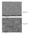
- FIGS. 5 a and 5 b are SEM micrographs of spray formed 37.1Cu-52.3In-10.6 wt. % Ga alloy.
- FIG. 5 a is a low magnification micrograph showing the entire thickness of a low porosity deposit on an aluminum backing tube.
- FIG. 5 b is a higher magnification micrograph showing a fine microstructure consisting primarily of Cu 9 (In,Ga) 4 and In phases.
- sputtering targets One consideration in selecting and developing sputtering targets is the material to be used in such sputtering targets. Various materials that initially appear to be attractive selections impose manufacturing challenges, particularly from a metallurgical standpoint and particularly when forming the material into a cylindrical or tubular shape. Another consideration is that many monolithic targets formed without a backing tube are not adequate to accommodate water cooling which is provided to the magnets and target assembly during a sputtering operation. Due to this, sputtering materials must often be either bonded to a backing tube or directly formed onto a backing tube, such as a backing tube made from stainless steel or other suitable material.
- An exemplary sputtering technique is magnetron sputtering which utilizes magnetrons.
- magnetron sputtering techniques such as planar magnetron sputtering and rotary magnetron sputtering are discussed in U.S. Pat. No. 7,544,884, issued on Jun. 9, 2009, and which is hereby incorporated by reference in its entirety.
- Rotary magnetron sputtering uses cylindrical sputtering targets that include a tube that forms the target material and at least one magnet located inside the tube. Due to the continuous displacement of the magnetic flux lines running through the tube wall as the tube is rotated around the magnets, circumferentially uniform erosion is achieved at the surface of the sputtering target. Such an erosion profile results in higher utilization of the target material in comparison to the erosion profiles provided by other sputtering techniques, such as those employing stationary, planar magnetrons.
- Copper indium selenide (“CIS”) and copper indium gallium selenide (“CIGS”) materials have been recognized as effective p-type solar cell absorber layer materials for the production of high efficiency, low cost, and large scale solar cells.
- Copper indium selenide and copper indium gallium selenide materials may be formed by a reactive sputtering from a copper indium or copper indium gallium (“CIG”) sputtering targets, respectively, in a selenium containing ambient, such as selenium gas or hydrogen selenide gas.
- a spray forming method is provided to produce a sputtering target.
- the spray forming method (which is also referred to as atomization) can be used to spray a liquid or melted sputtering target material, such as, for example, a copper indium gallium (“CIG”) alloy, directly onto a backing structure, such as a cylindrical backing tube.
- a liquid or melted sputtering target material such as, for example, a copper indium gallium (“CIG”) alloy
- CIG alloys possess a large freezing range, with a liquidus temperature over 500° C., often around 650° C., and a solidus temperature of below 160° C. A significant volume change is associated with the solidification and thermal contraction that often occurs over such a wide temperature range. Thus, a substantial amount of shrinkage occurs during conventional casting of such alloys.
- Sputtering targets long in one dimension, having narrow sections and thin walled features, for example, can have porosity due to extensive solidification shrinkage. Inclusions and structural defects, such as porosity, are detrimental to sputtering processes, because such defects can cause arcing and electrical discharges that result in particle generation and the development of thin film anomalies.
- Phase heterogeneities such as large areas of indium, can also be detrimental to the sputtering process, so it is desirable that the target material possess a fine-scale microstructure, which is obtained by employing sufficiently rapid cooling during solidification.
- large scale variations of composition within a target can lead to sputtered thin films of variable properties across their area and, as a consequence, reduced yield, so the method of CIG target production must limit the amount of macroscopic segregation of constituent elements.
- manufacturing sputtering targets employs powder metallurgical processing, pressing atomized powder under a combination of temperature and/or pressure, for example, techniques, which tend to be expensive and laborious.
- the CIG sputtering target material has a composition of about 29-41 wt % copper, including 29-39 wt % Cu, about 36-62 wt % indium, including 49-62 wt % In, and about 8-25 wt % gallium, including 16-25 wt % Ga.
- the CIG sputtering target material has a composition of about 8-15 wt % copper, about 55-80 wt % indium, and about 10-25 wt % gallium.
- the sputtering target material has an overall uniform composition, whereby the wt % of each of these 3 primary elements, of samples taken from any 2 random locations of the target, as determined by reliable analytical procedures of a material volume of at least 10 mm 3 , does not vary relatively by more than 5%, and more preferably not more than 2%, and yet more preferably not more than 1%.
- the microstructure of CIG consists of a Cu—Ga-rich intermetallic phase (or phases) in an indium-rich matrix. Depending primarily on the composition, the microstructure may contain additional minority phases, such as Cu, for example.
- the sizes of the primary phase regions are determined using the planimetric technique described in section 12.5 of ASTM standard E1382-97 (2004) and using ASTM E562-08 to calculate volume fraction, in each case substituting primary phase “region” for “grain”.
- Each primary phase “region” is defined as an entity visible in cross section under SEM with discernable boundaries and surrounded by the indium-rich matrix. In some cases, primary phase regions may have visible cracks but no matrix in the crack, in which case this is still counted as a single primary phase region.
- the primary phase regions are of size greater than 30 ⁇ m in a random 1 cm by 1 cm area of the sputtering target. More preferably, between 0% and 10%, for instance 1% to 5%, of the primary phase regions are of size greater than 10 ⁇ m.
- the average size of the primary phase region is no greater than 10 ⁇ m. More preferably, the average primary phase region size is 0.5 to 10 ⁇ m, such as 1 to 5 ⁇ m.
- the CIG sputtering target material has a density of 95% or more, as determined by the rule of mixtures applied to the densities of the component elements.
- the density determined this way can be greater than 100% due to the formation of an intermetallic compound with greater density than the pure elements.
- the sputtering target material has a density of about 95 to 107%, such as 100 to 107%.
- the average level of porosity in the CIG sputtering target material should be 0 to 12 vol %, as determined by microstructural image analysis of representative cross sections, for example. More preferably, the average level of porosity may be 0 to 7 vol %, such as 0.5 to 2.5 vol %.
- the CIG sputtering target material should not contain single inclusions or pores large enough to completely contain a 100 ⁇ m diameter sphere, preferably it should not contain single inclusions or pores large enough to completely contain a 50 ⁇ m sphere. In other words, single inclusions or pores, if present in the material, are small enough to only contain a sphere of less than 50 ⁇ m. Non limiting examples of single inclusions are foreign contaminants and/or oxide particles.
- the CIG sputtering target material should contain no pores or cracks having a distance of larger than 1000 ⁇ m when measured as straight linear distance between ends, more preferably not larger than 500 ⁇ m.
- a method of spray forming is provided to produce a sputtering target.
- a stream of molten CIG sputtering target material is provided by a crucible or tundish, which is then atomized by the impingement of high velocity inert gas jets, to form a spray, which is collected by a manipulated backing structure to build up a thick deposit, layer-wise as the spray is traversed numerous times, of the solid CIG sputtering target material on the backing structure, as shown in FIG. 1 for a tubular backing structure suitable for a rotary target.
- the total thickness of the sputtering target material can be controlled by the amount of melt deposited, resulting in a deposit that needs a minimum amount of machining to the precise dimensions required by the sputtering target.
- the heat of solidification is rapidly withdrawn from the molten CIG material by the gas, both before and after deposition, during flight of the spray droplets and on the top surface of the deposit. This enables the sputtering target material to be formed by rapid solidification of the liquid sputtering target material on the backing structure at a rate of greater than approximately 100° C./s.
- the resultant structure of the spray formed sputtering target material has many of the benefits of that conferred by powder metallurgical techniques, without the difficulties and extra process steps associated with powder handling, storage, classification and consolidation.
- FIG. 1 shows an example of an assembly for producing a rotary sputtering target.
- a crucible 25 can be provided to deliver molten sputtering target material 30 to a tundish 4 that has a nozzle 8 in the base.
- the molten material 30 may be delivered to the tundish via a conduit, such as a pipe, from a melt furnace.
- the tundish 4 may also act as a crucible, in which case the material 30 is delivered to the tundish 4 in the solid state and is then melted in the tundish 4 , by a surrounding induction coil, for example.
- the atomizer 14 can be of a close-coupled or a free-fall design.
- the backing tube 70 is rotated and translated (backwards and forwards) by a manipulator, such as in the direction indicated by the arrows X and Y in FIG. 1 , so that a coating 65 of sputtering target material with an even or uniform thickness is produced over the entire length of the backing tube 70 .
- the profile of the sputtering material deposit 65 can be varied in the longitudinal direction of the backing tube 70 (e.g., the axial direction) by varying the translational speed during each cycle, so that there can be excess sputtering target material 65 in areas where there is preferential removal during sputtering processes.
- the entire spray and deposition process is contained within an enclosed chamber, primarily to protect the spray and deposit from atmospheric contamination, such as oxidation, for example.
- the chamber aids the control of excess spray, overspray, and dust, preventing it from escaping into the surroundings.
- the melting arrangement of crucible and tundish is enclosed by a chamber, also to protect the melt from atmospheric contamination. It is preferred that a vacuum can be achieved inside both spray and melt chambers and they can be backfilled with an inert gas, such as argon or nitrogen.
- the temperature at the top surface of the deposit, around the point of deposition of the spray, is very important in determining the structure of the resultant sputtering target material.
- the temperature at the point of deposition is determined by the parameters employed for spray atomization, such as the melt temperature, the melt and gas flow rates, as examples, and the parameters employed for substrate manipulation, such as the spray distance and substrate transverse speed.
- the backing structure can be heated prior to spraying, so that the sputtering target material does not contain pores close to the backing structure and the bond strength is increased.
- the backing structure may be pre-heated by an external heating device, such as an electrical heater.
- the substrate manipulation system includes a method to cool the backing structure after the commencement of spraying, to prevent over heating of the deposit.
- a cooling method will also ensure that the entire sputtering target can be quickly returned to near ambient temperature after the termination of spraying, resulting in a short turn around time for efficient production.
- the backing structure/deposit temperature control may be provided by providing a cooling and/or heating device into the hollow interior of the tube.
- the cooling and/or heating device may comprise cooling or heating fluid conduit (such as a cold and/or hot water pipes), a resistive heater, inductive coils, etc.
- the provision of backing structure/deposit temperature control has the added advantage of being able to prevent deposit cracking that would otherwise be induced by differences in thermal contraction between the deposit and the backing structure.
- the surface of the backing structure to be deposited on to should be prepared so that the initial sprayed sputtering target material can adhere.
- the backing structure surface may be roughened by a process such as grit blasting, for example, whereby an abrasive particulate, such as alumina, for example, is blasted at the surface using compressed air. It maybe necessary to enhance the bond strength between the spray formed sputtering target material and the backing structure by increasing the roughness of the surface further, by coating the backing structure with any suitable thin, non-magnetic layer, applied by twin wire electric arc spray, for example, using parameters familiar to those skilled in the art.
- a traverse speed of the spray across the substrate that is too slow can cause excessive porosity in the target material, typically appearing as bands, due to problems associated with a deposition layer per spray pass that is too thick and/or deposition occurring on a top surface that is too cold.
- a substrate manipulation system both translates (along the axis of the tube) in a reciprocating manner and rotates the tube about its axis at speeds so that a thin layer is deposited on each pass and restrict the formation of such pores.
- spreading of the deposition area over the backing structure can be increased for example, by scanning the spray, or by altering the atomizing gas flows or mechanical manipulation of the atomization die.
- a gas atomizer design that generates a spray that is essentially or substantially planar.
- the spray produced by the gas atomizer can be arranged to have about the same length as the object to be coated (i.e., the difference in length is 0-10% for example).
- the length of the spray can be the length of the long dimension of the backing structure.
- the length of the spray can be the axial length of the tube.
- the backing structure such as a backing tube
- the backing structure need only be moved or rotated in a single direction relative to the spray to form a built up layer of evenly deposited target material.
- a cylindrical backing tube can simply be rotated around its axis.
- the spray of liquid material may be provided from a single, linear opening to cover the whole length of the backing tube.
- the spray may be provided from plural adjacent openings at the same time.
- the arrangement of gas atomizing jets can be specifically designed to change properties of the spray, such as to change the size of the droplets of the spray, or the local melt flow rate, for example.
- the gas atomizing jets can be supplied with gas from independent sources to provide various spray conditions.
- the gas atomizing jets can be altered such that a region at the center of a deposit formed by the metal spray is formed under relatively colder conditions than regions at the ends of the deposit formed by the metal spray, thus countering effects of external cooling of the deposit.
- the jets may comprise any suitable gas that does not compromise the structure or composition, by the formation of oxides, for example, of the sputtering target material, such as argon, nitrogen, etc.
- FIG. 2 a shows an exemplary linear atomization assembly for spray forming 10 that includes a tundish 20 .
- a source of molten sputtering target material (not shown in FIG. 2 a ) can be provided to deliver molten sputtering target material 30 (e.g., liquid CIG alloy) to the tundish 20 .
- the tundish 20 can have a linear slot-like nozzle or opening 40 from which the molten sputtering target material 30 flows.
- An array of gas jets 55 can surround the nozzle 40 so that gas G supplied from a manifold 50 can exit the gas jets 55 and impact a stream of molten sputtering target material exiting the nozzle 40 of the tundish 20 , producing a spray of sputtering target material droplets 60 .
- the spray of droplets 60 can be deposited to form or build up a sputtering target, such as by building up the spray of solidified droplets, layer by layer, on a backing structure, such as a planar or rotary (e.g., tubular) backing structure.
- a backing structure such as a planar or rotary (e.g., tubular) backing structure.
- Such an atomizer could be either of a close-coupled or a free fall design.
- the axis of the spray 60 produced by the atomizer assembly can be essentially or substantially planar.
- Such profile can be provided by the shape of the tundish nozzle 40 , which can be elongated in one direction to provide a slot-like opening, such as in the design shown in the example of FIG. 2 b , and/or by the arrangement of gas jets 55 surrounding the nozzle opening 40 .
- FIG. 2 c shows an example of an assembly for producing a rotary sputtering target with a linear atomizer.
- a crucible 25 can be provided to deliver molten sputtering target material 30 to a tundish 20 that has a nozzle 40 .
- the molten material 30 may be delivered to the tundish via a conduit, such as a pipe, from a melt furnace.
- the tundish 20 may also act as a melt furnace, in which case the material 30 is delivered to the tundish 20 in the solid state and is then melted in the tundish.
- the nozzle 40 can have a linearly shaped slot, as discussed herein, and can be surrounded by gas jets (not shown in FIG.
- the spray of metal droplets 60 can then be deposited onto a backing tube 70 by aligning a long axis of the nozzle 40 with the long axis of the backing tube 70 , as shown in the example of FIG. 2 c.
- the backing tube 70 can be rotated, such as in the direction indicated by arrow X in FIG. 2 c , so that a coating 65 of sputtering target material with an even or uniform thickness is produced over the entire length of backing tube 70 .
- the backing tube 70 can be advantageously rotated without additional translation of the backing tube 70 , such as without translating the backing tube 70 in the direction of the long axis of the backing tube 70 in relation to the spray of metal droplets 60 .
- the deposition profile of the metal spray 60 can be varied in the longitudinal direction of the backing tube 70 (e.g., the axial direction) by varying a width of the nozzle or opening 40 of the spray/atomization device.
- the profile of the metal spray 60 can be varied in the longitudinal direction to deposit excess sputtering target material 65 in areas where there is preferential removal during sputtering processes.
- the width of the nozzle or opening 40 in the tundish 20 is wider in regions which overlying the portions of the target requiring excess target material 65 .
- the assembly for producing a rotary sputtering target by spray forming using a linear atomization arrangement does not require equipment to translate a backing tube 70 in addition to equipment to rotate the backing tube 70 . This simplifies the design and fabrication of the assembly, particularly if the assembly includes heating and/or cooling equipment. The simplification of the design of the assembly also results in a smaller effective size of the overall assembly, which in turn reduces the overall size of a spray forming chamber for the assembly, such as when the spray forming apparatus is provided within a chamber to provide a controlled environment, such as a vacuum or an inert gas (e.g., argon) atmosphere.
- a controlled environment such as a vacuum or an inert gas (e.g., argon) atmosphere.
- a mixture of metals and/or metal alloy(s), such as, for example, a CIG alloy, is melted in a vessel to provide a uniform composition.
- the molten material supply may be manipulated such that one or more elements in the melt (e.g., Cu, In, Ga, Na, Zn and/or Al) has a controlled composition gradient with respect to the space of the melt.
- elements in the melt e.g., Cu, In, Ga, Na, Zn and/or Al
- a controlled composition gradient permits flexibility with the variables of the spray forming process.
- sodium may be added to the copper indium gallium melt.
- One or more elements may be added to the melt, such as by a continuous or batch metering device, to provide a changing gradient of composition within the geometry of the melt.
- the composition of the melt 30 in FIGS. 1 and 2 c ) may be non-uniform in the vertical direction in the tundish 4 or 20 .
- the melt 30 of one composition may be completely discharged from the tundish 4 or 20 followed by filling the tundish with a melt of a different composition.
- a sputtering target is produced with a high density, low porosity, a composition with a high uniformity and a fine scale microstructure.
- the spray forming method is flexible in that the melt temperature, nozzle sizes and geometries, melt flow rate, atomizer designs and geometries, gas flow rates, gas temperatures, melt chamber geometry, backing structure thermal management, and motion of the backing structure can all be controlled to achieve a desired solidification rate of the droplets during flight and after deposition. If necessary, the resulting combination of backing structure and coating may then be subjected to post-process treatment, such as treatments under relatively higher temperatures and pressure to change the coating structure. For example, the spray formed sputtering target material maybe sheared, using an extrusion press and die arrangement, to close any residual porosity.
- Post-deposition processing can include other processes, such as, for example, abrasive, ablative, or electrolytic removal of an outer layer of the coating material, and other processes used in the art.
- a rotary (i.e., tubular) target was described above, it should be noted that other target shapes may be formed.
- a planar target may be formed instead by using a planar backing structure in the methods of FIG. 1 or FIG. 2C .
- the planar backing structure may be translated in two dimensions or one dimension in the methods of FIGS. 1 and 2C , respectively.
- the present invention is not limited to the embodiment(s) and the example(s) described above and illustrated herein, but encompasses any and all variations falling within the scope of the appended claims.
- the CIG alloy may contain other alloying elements.
- the alloy may contain Na, Al, S and/or Se in addition to copper, indium and gallium.
- the CIG alloy melt may comprise a Na-containing material such that it contains 0.01 wt % to 10 wt % Na, for example 0.1 wt % to 1.0 wt %.
- the sodium-containing material may comprise any material containing sodium, for example metallic sodium or alloys or compounds of sodium with one or more of selenium, sulfur, oxygen, nitrogen or barrier metal (such as molybdenum, tungsten, tantalum, vanadium, titanium, niobium or zirconium), such as sodium fluoride, sodium molybdate, sodium fluoride, sodium selenide, sodium hydroxide, sodium oxide, sodium sulfate, sodium tungstate, sodium selenate, sodium selenite, sodium sulfide, sodium sulfite, sodium titanate, sodium metavanadate, sodium orthovanadate, or combinations thereof.
- barrier metal such as molybdenum, tungsten, tantalum, vanadium, titanium, niobium or zirconium
- barrier metal such as molybdenum, tungsten, tantalum, vanadium, titanium, niobium or zirconium
- barrier metal such as molybdenum, tungsten, tanta
- Alloys or compounds of lithium and/or potassium may be also used, for example but not limited to alloys or compounds of lithium or potassium with one or more of selenium, sulfur, oxygen, nitrogen, molybdenum, tungsten, tantalum, vanadium, titanium, niobium or zirconium.
- Additional elements can also be incorporated into the spray formed CIG target by introducing particulate (i.e., solid particles) into the liquid spray so as to create a substantially homogenous distribution of particles within the target. This is achieved by seeding a secondary gas flow with particles and injecting them at a point, or points, close to the atomization die on the axis of the spray. Typically, the injection needs to be symmetrically arranged, or in an annulus, around the spray axis to ensure an even distribution of the particulate.
- the particulate can be of any material. For example, if Na is to be added to the target, the particulate can be a Na-containing compound, such as a Na-containing salt, such as NaCl.
- FIGS. 3 a - 3 c , 4 a - b and 5 a - b are SEM micrographs of various exemplary spray formed CIG alloys.
- FIGS. 3 a - 3 c are micrographs of a low Cu content CIG alloy (8.6Cu-72.5In-18.9 wt. % Ga) spray formed on an Al-bronze bond coat on a steel backing tube.
- FIGS. 4 a and 4 b are micrographs of an intermediate Cu content CIG alloy (33.4Cu-52.8In-13.8 wt. % Ga alloy) spray formed on a stainless steel backing tube.
- FIGS. 5 a and 5 b are micrographs of a high Cu content CIG alloy (37.1Cu-52.3In-10.6 wt. % Ga) spray formed on an aluminum backing tube.
Abstract
Description
Claims (22)
Priority Applications (1)
| Application Number | Priority Date | Filing Date | Title |
|---|---|---|---|
| US12/907,783 US8709548B1 (en) | 2009-10-20 | 2010-10-19 | Method of making a CIG target by spray forming |
Applications Claiming Priority (2)
| Application Number | Priority Date | Filing Date | Title |
|---|---|---|---|
| US27268109P | 2009-10-20 | 2009-10-20 | |
| US12/907,783 US8709548B1 (en) | 2009-10-20 | 2010-10-19 | Method of making a CIG target by spray forming |
Publications (1)
| Publication Number | Publication Date |
|---|---|
| US8709548B1 true US8709548B1 (en) | 2014-04-29 |
Family
ID=50514196
Family Applications (1)
| Application Number | Title | Priority Date | Filing Date |
|---|---|---|---|
| US12/907,783 Active 2032-07-03 US8709548B1 (en) | 2009-10-20 | 2010-10-19 | Method of making a CIG target by spray forming |
Country Status (1)
| Country | Link |
|---|---|
| US (1) | US8709548B1 (en) |
Cited By (4)
| Publication number | Priority date | Publication date | Assignee | Title |
|---|---|---|---|---|
| US20140264988A1 (en) * | 2013-03-15 | 2014-09-18 | The Government Of The United States Of America, As Represented By The Secretary Of The Navy | Photovoltaic sputtering targets fabricated from reclaimed materials |
| EP3456857A4 (en) * | 2017-08-04 | 2019-03-27 | Miasolé Equipment Integration (Fujian) Co., Ltd. | Method for preparing target material and target material |
| US10392693B2 (en) * | 2015-03-30 | 2019-08-27 | Jx Nippon Mining & Metals Corporation | Laminate structure and manufacturing method thereof |
| CN114250461A (en) * | 2021-12-13 | 2022-03-29 | 广东省科学院新材料研究所 | Rotary rare earth target material and preparation method and application thereof |
Citations (90)
| Publication number | Priority date | Publication date | Assignee | Title |
|---|---|---|---|---|
| US3902544A (en) | 1974-07-10 | 1975-09-02 | Massachusetts Inst Technology | Continuous process for forming an alloy containing non-dendritic primary solids |
| US3948650A (en) | 1972-05-31 | 1976-04-06 | Massachusetts Institute Of Technology | Composition and methods for preparing liquid-solid alloys for casting and casting methods employing the liquid-solid alloys |
| US4089680A (en) | 1976-09-22 | 1978-05-16 | Massachusetts Institute Of Technology | Method and apparatus for forming ferrous liquid-solid metal compositions |
| US4103730A (en) | 1974-07-22 | 1978-08-01 | Union Siderurgique Du Nord Et De L'est De La France | Process for electromagnetic stirring |
| US4150712A (en) | 1977-03-03 | 1979-04-24 | Union Siderurgique Du Nord Et De L'est De La France | Continuous-casting mould provided with an electromagnetic stirring device |
| US4178979A (en) | 1976-07-13 | 1979-12-18 | Institut De Recherches De La Siderurgie Francaise | Method of and apparatus for electromagnetic mixing of metal during continuous casting |
| US4200137A (en) | 1975-04-22 | 1980-04-29 | Republic Steel Corporation | Process and apparatus for the continuous casting of metal using electromagnetic stirring |
| US4229210A (en) | 1977-12-12 | 1980-10-21 | Olin Corporation | Method for the preparation of thixotropic slurries |
| US4356073A (en) | 1981-02-12 | 1982-10-26 | Shatterproof Glass Corporation | Magnetron cathode sputtering apparatus |
| US5302414A (en) | 1990-05-19 | 1994-04-12 | Anatoly Nikiforovich Papyrin | Gas-dynamic spraying method for applying a coating |
| US5343926A (en) * | 1991-01-02 | 1994-09-06 | Olin Corporation | Metal spray forming using multiple nozzles |
| US5401539A (en) * | 1985-11-12 | 1995-03-28 | Osprey Metals Limited | Production of metal spray deposits |
| US5435965A (en) | 1991-02-19 | 1995-07-25 | Mitsubishi Materials Corporation | Sputtering target and method for manufacturing same |
| US5522535A (en) | 1994-11-15 | 1996-06-04 | Tosoh Smd, Inc. | Methods and structural combinations providing for backing plate reuse in sputter target/backing plate assemblies |
| US5626688A (en) | 1994-12-01 | 1997-05-06 | Siemens Aktiengesellschaft | Solar cell with chalcopyrite absorber layer |
| US5699850A (en) | 1993-01-15 | 1997-12-23 | J. Mulcahy Enterprises Inc. | Method and apparatus for control of stirring in continuous casting of metals |
| US5814195A (en) | 1995-04-25 | 1998-09-29 | The Boc Group, Inc. | Sputtering system using cylindrical rotating magnetron electrically powered using alternating current |
| EP0881695A2 (en) | 1997-05-16 | 1998-12-02 | International Solar Electric Technology, Inc. | A method of making group IB-IIIA-VIA compund semiconductor films and method of fabricating a photovoltaic device |
| US5904966A (en) | 1993-09-24 | 1999-05-18 | Innovative Sputtering Technology N.V. (I.S.T.) | Laminated metal structure |
| US6020556A (en) | 1998-09-07 | 2000-02-01 | Honda Giken Kogyo Kabushiki Kaisha | Solar cell |
| US6070643A (en) | 1997-09-12 | 2000-06-06 | Howmet Research Corporation | High vacuum die casting |
| US6310281B1 (en) | 2000-03-16 | 2001-10-30 | Global Solar Energy, Inc. | Thin-film, flexible photovoltaic module |
| US20020033135A1 (en) | 2001-05-02 | 2002-03-21 | Asb Industries, Inc. | Cold spray system nozzle |
| US6372538B1 (en) | 2000-03-16 | 2002-04-16 | University Of Delaware | Fabrication of thin-film, flexible photovoltaic module |
| US6478842B1 (en) | 2000-07-19 | 2002-11-12 | R. A. Brands, Llc | Preparation of articles using metal injection molding |
| US6500733B1 (en) | 2001-09-20 | 2002-12-31 | Heliovolt Corporation | Synthesis of layers, coatings or films using precursor layer exerted pressure containment |
| US6525264B2 (en) | 2000-07-21 | 2003-02-25 | Sharp Kabushiki Kaisha | Thin-film solar cell module |
| US6559372B2 (en) | 2001-09-20 | 2003-05-06 | Heliovolt Corporation | Photovoltaic devices and compositions for use therein |
| US6593213B2 (en) | 2001-09-20 | 2003-07-15 | Heliovolt Corporation | Synthesis of layers, coatings or films using electrostatic fields |
| US6690041B2 (en) | 2002-05-14 | 2004-02-10 | Global Solar Energy, Inc. | Monolithically integrated diodes in thin-film photovoltaic devices |
| US6736986B2 (en) | 2001-09-20 | 2004-05-18 | Heliovolt Corporation | Chemical synthesis of layers, coatings or films using surfactants |
| US6739384B2 (en) | 2001-09-13 | 2004-05-25 | Ak Properties, Inc. | Method of continuously casting electrical steel strip with controlled spray cooling |
| US6750394B2 (en) | 2001-01-12 | 2004-06-15 | Sharp Kabushiki Kaisha | Thin-film solar cell and its manufacturing method |
| US6787692B2 (en) | 2000-10-31 | 2004-09-07 | National Institute Of Advanced Industrial Science & Technology | Solar cell substrate, thin-film solar cell, and multi-junction thin-film solar cell |
| US6822158B2 (en) | 2002-03-11 | 2004-11-23 | Sharp Kabushiki Kaisha | Thin-film solar cell and manufacture method therefor |
| US6852920B2 (en) | 2002-06-22 | 2005-02-08 | Nanosolar, Inc. | Nano-architected/assembled solar electricity cell |
| US6878612B2 (en) | 2002-09-16 | 2005-04-12 | Oki Electric Industry Co., Ltd. | Self-aligned contact process for semiconductor device |
| US6881647B2 (en) | 2001-09-20 | 2005-04-19 | Heliovolt Corporation | Synthesis of layers, coatings or films using templates |
| US20050109392A1 (en) * | 2002-09-30 | 2005-05-26 | Hollars Dennis R. | Manufacturing apparatus and method for large-scale production of thin-film solar cells |
| US6936761B2 (en) | 2003-03-29 | 2005-08-30 | Nanosolar, Inc. | Transparent electrode, optoelectronic apparatus and devices |
| US20050194036A1 (en) * | 2004-03-01 | 2005-09-08 | Basol Bulent M. | Low cost and high throughput deposition methods and apparatus for high density semiconductor film growth |
| US20050202589A1 (en) * | 2004-03-15 | 2005-09-15 | Basol Bulent M. | Technique and apparatus for depositing thin layers of semiconductors for solar cell fabrication |
| US6987071B1 (en) | 2003-11-21 | 2006-01-17 | Nanosolar, Inc. | Solvent vapor infiltration of organic materials into nanostructures |
| US7045205B1 (en) | 2004-02-19 | 2006-05-16 | Nanosolar, Inc. | Device based on coated nanoporous structure |
| US7115304B2 (en) | 2004-02-19 | 2006-10-03 | Nanosolar, Inc. | High throughput surface treatment on coiled flexible substrates |
| US7122392B2 (en) | 2003-06-30 | 2006-10-17 | Intel Corporation | Methods of forming a high germanium concentration silicon germanium alloy by epitaxial lateral overgrowth and structures formed thereby |
| US7122398B1 (en) | 2004-03-25 | 2006-10-17 | Nanosolar, Inc. | Manufacturing of optoelectronic devices |
| US7141449B2 (en) | 2002-06-07 | 2006-11-28 | Honda Giken Kogyo Kabushiki Kaisha | Method of fabricating a compound semiconductor thin-layer solar cell |
| US7163608B2 (en) | 2001-09-20 | 2007-01-16 | Heliovolt Corporation | Apparatus for synthesis of layers, coatings or films |
| US7194197B1 (en) | 2000-03-16 | 2007-03-20 | Global Solar Energy, Inc. | Nozzle-based, vapor-phase, plume delivery structure for use in production of thin-film deposition layer |
| US7196262B2 (en) | 2005-06-20 | 2007-03-27 | Solyndra, Inc. | Bifacial elongated solar cell devices |
| US20070074969A1 (en) | 2005-10-03 | 2007-04-05 | Simpson Wayne R | Very long cylindrical sputtering target and method for manufacturing |
| US20070093059A1 (en) * | 2005-10-24 | 2007-04-26 | Basol Bulent M | Method And Apparatus For Thin Film Solar Cell Manufacturing |
| US7227066B1 (en) | 2004-04-21 | 2007-06-05 | Nanosolar, Inc. | Polycrystalline optoelectronic devices based on templating technique |
| US7235736B1 (en) | 2006-03-18 | 2007-06-26 | Solyndra, Inc. | Monolithic integration of cylindrical solar cells |
| US7247346B1 (en) | 2002-08-28 | 2007-07-24 | Nanosolar, Inc. | Combinatorial fabrication and high-throughput screening of optoelectronic devices |
| US7253017B1 (en) | 2002-06-22 | 2007-08-07 | Nanosolar, Inc. | Molding technique for fabrication of optoelectronic devices |
| US7259322B2 (en) | 2006-01-09 | 2007-08-21 | Solyndra, Inc. | Interconnects for solar cell devices |
| US7262392B1 (en) | 2004-09-18 | 2007-08-28 | Nanosolar, Inc. | Uniform thermal processing by internal impedance heating of elongated substrates |
| US7267724B2 (en) | 2000-06-23 | 2007-09-11 | Anelva Corporation | Thin-film disposition apparatus |
| US7271333B2 (en) | 2001-07-20 | 2007-09-18 | Ascent Solar Technologies, Inc. | Apparatus and method of production of thin film photovoltaic modules |
| US7291782B2 (en) | 2002-06-22 | 2007-11-06 | Nanosolar, Inc. | Optoelectronic device and fabrication method |
| US7306823B2 (en) | 2004-09-18 | 2007-12-11 | Nanosolar, Inc. | Coated nanoparticles and quantum dots for solution-based fabrication of photovoltaic cells |
| US20070283996A1 (en) | 2006-06-13 | 2007-12-13 | Miasole | Photovoltaic module with insulating interconnect carrier |
| US20070283997A1 (en) | 2006-06-13 | 2007-12-13 | Miasole | Photovoltaic module with integrated current collection and interconnection |
| US20080000518A1 (en) | 2006-03-28 | 2008-01-03 | Basol Bulent M | Technique for Manufacturing Photovoltaic Modules |
| US7319190B2 (en) | 2004-11-10 | 2008-01-15 | Daystar Technologies, Inc. | Thermal process for creation of an in-situ junction layer in CIGS |
| US20080053519A1 (en) | 2006-08-30 | 2008-03-06 | Miasole | Laminated photovoltaic cell |
| US20080105542A1 (en) | 2006-11-08 | 2008-05-08 | Purdy Clifford C | System and method of manufacturing sputtering targets |
| US20080121137A1 (en) * | 2006-11-23 | 2008-05-29 | Van Osten Karl-Uwe | Coating material based on a copper-indium-gallium alloy, in particular for the production of sputter targets, tubular cathodes and the like |
| US20080145692A1 (en) | 2006-12-04 | 2008-06-19 | Heraeus Inc. | Magnetic pulse-assisted casting of metal alloys & metal alloys produced thereby |
| US20080142071A1 (en) | 2006-12-15 | 2008-06-19 | Miasole | Protovoltaic module utilizing a flex circuit for reconfiguration |
| US20080271781A1 (en) | 2004-12-09 | 2008-11-06 | Showa Shell Sekiyu K. K. | Cis Type Thin-Film Solar Cell and Process for Producing the Same |
| US20080271779A1 (en) | 2007-05-04 | 2008-11-06 | H.C. Starck Inc. | Fine Grained, Non Banded, Refractory Metal Sputtering Targets with a Uniformly Random Crystallographic Orientation, Method for Making Such Film, and Thin Film Based Devices and Products Made Therefrom |
| US20080314432A1 (en) | 2007-06-19 | 2008-12-25 | Miasole | Photovoltaic module utilizing an integrated flex circuit and incorporating a bypass diode |
| US20090014057A1 (en) | 2007-07-13 | 2009-01-15 | Miasole | Photovoltaic modules with integrated devices |
| US20090014049A1 (en) | 2007-07-13 | 2009-01-15 | Miasole | Photovoltaic module with integrated energy storage |
| US20090014058A1 (en) | 2007-07-13 | 2009-01-15 | Miasole | Rooftop photovoltaic systems |
| JP2009120862A (en) | 2007-11-12 | 2009-06-04 | Mitsubishi Materials Corp | Cu-In-Ga TERNARY SINTERED ALLOY SPUTTERING TARGET, AND ITS MANUFACTURING METHOD |
| JP2009120863A (en) | 2007-11-12 | 2009-06-04 | Mitsubishi Materials Corp | MANUFACTURING METHOD OF Cu-In-Ga TERNARY SINTERED ALLOY SPUTTERING TARGET |
| US20090199894A1 (en) | 2007-12-14 | 2009-08-13 | Miasole | Photovoltaic devices protected from environment |
| US20090223556A1 (en) | 2005-12-21 | 2009-09-10 | Thomas Niesen | Process of making a thin-film photovoltaic device and thin-film photovoltaic device |
| US7637441B2 (en) | 2006-03-24 | 2009-12-29 | Linde Aktiengesellschaft | Cold gas spray gun |
| US20100116341A1 (en) | 2008-11-12 | 2010-05-13 | Solar Applied Materials Technology Corp. | Copper-gallium allay sputtering target, method for fabricating the same and related applications |
| US20100133093A1 (en) | 2009-04-13 | 2010-06-03 | Mackie Neil M | Method for alkali doping of thin film photovoltaic materials |
| US20100136242A1 (en) | 2008-12-03 | 2010-06-03 | Albert Kay | Spray nozzle assembly for gas dynamic cold spray and method of coating a substrate with a high temperature coating |
| US20100212732A1 (en) | 2009-02-20 | 2010-08-26 | Miasole | Protective layer for large-scale production of thin-film solar cells |
| US20100212733A1 (en) | 2009-02-20 | 2010-08-26 | Miasole | Protective layer for large-scale production of thin-film solar cells |
| US7785921B1 (en) | 2009-04-13 | 2010-08-31 | Miasole | Barrier for doped molybdenum targets |
| US20110089030A1 (en) | 2009-10-20 | 2011-04-21 | Miasole | CIG sputtering target and methods of making and using thereof |
-
2010
- 2010-10-19 US US12/907,783 patent/US8709548B1/en active Active
Patent Citations (98)
| Publication number | Priority date | Publication date | Assignee | Title |
|---|---|---|---|---|
| US3948650A (en) | 1972-05-31 | 1976-04-06 | Massachusetts Institute Of Technology | Composition and methods for preparing liquid-solid alloys for casting and casting methods employing the liquid-solid alloys |
| US3902544A (en) | 1974-07-10 | 1975-09-02 | Massachusetts Inst Technology | Continuous process for forming an alloy containing non-dendritic primary solids |
| US4103730A (en) | 1974-07-22 | 1978-08-01 | Union Siderurgique Du Nord Et De L'est De La France | Process for electromagnetic stirring |
| US4200137A (en) | 1975-04-22 | 1980-04-29 | Republic Steel Corporation | Process and apparatus for the continuous casting of metal using electromagnetic stirring |
| US4178979A (en) | 1976-07-13 | 1979-12-18 | Institut De Recherches De La Siderurgie Francaise | Method of and apparatus for electromagnetic mixing of metal during continuous casting |
| US4089680A (en) | 1976-09-22 | 1978-05-16 | Massachusetts Institute Of Technology | Method and apparatus for forming ferrous liquid-solid metal compositions |
| US4150712A (en) | 1977-03-03 | 1979-04-24 | Union Siderurgique Du Nord Et De L'est De La France | Continuous-casting mould provided with an electromagnetic stirring device |
| US4229210A (en) | 1977-12-12 | 1980-10-21 | Olin Corporation | Method for the preparation of thixotropic slurries |
| US4356073A (en) | 1981-02-12 | 1982-10-26 | Shatterproof Glass Corporation | Magnetron cathode sputtering apparatus |
| US5401539A (en) * | 1985-11-12 | 1995-03-28 | Osprey Metals Limited | Production of metal spray deposits |
| US5302414B1 (en) | 1990-05-19 | 1997-02-25 | Anatoly N Papyrin | Gas-dynamic spraying method for applying a coating |
| US5302414A (en) | 1990-05-19 | 1994-04-12 | Anatoly Nikiforovich Papyrin | Gas-dynamic spraying method for applying a coating |
| US5343926A (en) * | 1991-01-02 | 1994-09-06 | Olin Corporation | Metal spray forming using multiple nozzles |
| US5435965A (en) | 1991-02-19 | 1995-07-25 | Mitsubishi Materials Corporation | Sputtering target and method for manufacturing same |
| US5699850A (en) | 1993-01-15 | 1997-12-23 | J. Mulcahy Enterprises Inc. | Method and apparatus for control of stirring in continuous casting of metals |
| US5904966A (en) | 1993-09-24 | 1999-05-18 | Innovative Sputtering Technology N.V. (I.S.T.) | Laminated metal structure |
| US5522535A (en) | 1994-11-15 | 1996-06-04 | Tosoh Smd, Inc. | Methods and structural combinations providing for backing plate reuse in sputter target/backing plate assemblies |
| US5626688A (en) | 1994-12-01 | 1997-05-06 | Siemens Aktiengesellschaft | Solar cell with chalcopyrite absorber layer |
| US5814195A (en) | 1995-04-25 | 1998-09-29 | The Boc Group, Inc. | Sputtering system using cylindrical rotating magnetron electrically powered using alternating current |
| DE69835851T2 (en) | 1997-05-16 | 2007-04-12 | International Solar Electric Technology, Inc., Chatsworth | Process for the preparation of thin films from group IB-IIIA-VIA compound semiconductors and process for the production of a photovoltaic device |
| EP0881695A2 (en) | 1997-05-16 | 1998-12-02 | International Solar Electric Technology, Inc. | A method of making group IB-IIIA-VIA compund semiconductor films and method of fabricating a photovoltaic device |
| US6070643A (en) | 1997-09-12 | 2000-06-06 | Howmet Research Corporation | High vacuum die casting |
| US6020556A (en) | 1998-09-07 | 2000-02-01 | Honda Giken Kogyo Kabushiki Kaisha | Solar cell |
| US6372538B1 (en) | 2000-03-16 | 2002-04-16 | University Of Delaware | Fabrication of thin-film, flexible photovoltaic module |
| US7194197B1 (en) | 2000-03-16 | 2007-03-20 | Global Solar Energy, Inc. | Nozzle-based, vapor-phase, plume delivery structure for use in production of thin-film deposition layer |
| US6310281B1 (en) | 2000-03-16 | 2001-10-30 | Global Solar Energy, Inc. | Thin-film, flexible photovoltaic module |
| US7267724B2 (en) | 2000-06-23 | 2007-09-11 | Anelva Corporation | Thin-film disposition apparatus |
| US6478842B1 (en) | 2000-07-19 | 2002-11-12 | R. A. Brands, Llc | Preparation of articles using metal injection molding |
| US6525264B2 (en) | 2000-07-21 | 2003-02-25 | Sharp Kabushiki Kaisha | Thin-film solar cell module |
| US6787692B2 (en) | 2000-10-31 | 2004-09-07 | National Institute Of Advanced Industrial Science & Technology | Solar cell substrate, thin-film solar cell, and multi-junction thin-film solar cell |
| US6750394B2 (en) | 2001-01-12 | 2004-06-15 | Sharp Kabushiki Kaisha | Thin-film solar cell and its manufacturing method |
| US20020033135A1 (en) | 2001-05-02 | 2002-03-21 | Asb Industries, Inc. | Cold spray system nozzle |
| US6722584B2 (en) | 2001-05-02 | 2004-04-20 | Asb Industries, Inc. | Cold spray system nozzle |
| US7271333B2 (en) | 2001-07-20 | 2007-09-18 | Ascent Solar Technologies, Inc. | Apparatus and method of production of thin film photovoltaic modules |
| US6739384B2 (en) | 2001-09-13 | 2004-05-25 | Ak Properties, Inc. | Method of continuously casting electrical steel strip with controlled spray cooling |
| US6559372B2 (en) | 2001-09-20 | 2003-05-06 | Heliovolt Corporation | Photovoltaic devices and compositions for use therein |
| US7148123B2 (en) | 2001-09-20 | 2006-12-12 | Heliovolt Corporation | Synthesis of layers, coatings or films using collection layer |
| US6500733B1 (en) | 2001-09-20 | 2002-12-31 | Heliovolt Corporation | Synthesis of layers, coatings or films using precursor layer exerted pressure containment |
| US7163608B2 (en) | 2001-09-20 | 2007-01-16 | Heliovolt Corporation | Apparatus for synthesis of layers, coatings or films |
| US6797874B2 (en) | 2001-09-20 | 2004-09-28 | Heliovolt Corporation | Layers, coatings or films synthesized using precursor layer exerted pressure containment |
| US6881647B2 (en) | 2001-09-20 | 2005-04-19 | Heliovolt Corporation | Synthesis of layers, coatings or films using templates |
| US6593213B2 (en) | 2001-09-20 | 2003-07-15 | Heliovolt Corporation | Synthesis of layers, coatings or films using electrostatic fields |
| US6736986B2 (en) | 2001-09-20 | 2004-05-18 | Heliovolt Corporation | Chemical synthesis of layers, coatings or films using surfactants |
| US6822158B2 (en) | 2002-03-11 | 2004-11-23 | Sharp Kabushiki Kaisha | Thin-film solar cell and manufacture method therefor |
| US6690041B2 (en) | 2002-05-14 | 2004-02-10 | Global Solar Energy, Inc. | Monolithically integrated diodes in thin-film photovoltaic devices |
| US7141449B2 (en) | 2002-06-07 | 2006-11-28 | Honda Giken Kogyo Kabushiki Kaisha | Method of fabricating a compound semiconductor thin-layer solar cell |
| US7291782B2 (en) | 2002-06-22 | 2007-11-06 | Nanosolar, Inc. | Optoelectronic device and fabrication method |
| US7253017B1 (en) | 2002-06-22 | 2007-08-07 | Nanosolar, Inc. | Molding technique for fabrication of optoelectronic devices |
| US6852920B2 (en) | 2002-06-22 | 2005-02-08 | Nanosolar, Inc. | Nano-architected/assembled solar electricity cell |
| US7247346B1 (en) | 2002-08-28 | 2007-07-24 | Nanosolar, Inc. | Combinatorial fabrication and high-throughput screening of optoelectronic devices |
| US6878612B2 (en) | 2002-09-16 | 2005-04-12 | Oki Electric Industry Co., Ltd. | Self-aligned contact process for semiconductor device |
| US20050109392A1 (en) * | 2002-09-30 | 2005-05-26 | Hollars Dennis R. | Manufacturing apparatus and method for large-scale production of thin-film solar cells |
| US7544884B2 (en) | 2002-09-30 | 2009-06-09 | Miasole | Manufacturing method for large-scale production of thin-film solar cells |
| US6936761B2 (en) | 2003-03-29 | 2005-08-30 | Nanosolar, Inc. | Transparent electrode, optoelectronic apparatus and devices |
| US7122392B2 (en) | 2003-06-30 | 2006-10-17 | Intel Corporation | Methods of forming a high germanium concentration silicon germanium alloy by epitaxial lateral overgrowth and structures formed thereby |
| US6987071B1 (en) | 2003-11-21 | 2006-01-17 | Nanosolar, Inc. | Solvent vapor infiltration of organic materials into nanostructures |
| US7115304B2 (en) | 2004-02-19 | 2006-10-03 | Nanosolar, Inc. | High throughput surface treatment on coiled flexible substrates |
| US7045205B1 (en) | 2004-02-19 | 2006-05-16 | Nanosolar, Inc. | Device based on coated nanoporous structure |
| US20050194036A1 (en) * | 2004-03-01 | 2005-09-08 | Basol Bulent M. | Low cost and high throughput deposition methods and apparatus for high density semiconductor film growth |
| US20050202589A1 (en) * | 2004-03-15 | 2005-09-15 | Basol Bulent M. | Technique and apparatus for depositing thin layers of semiconductors for solar cell fabrication |
| US7374963B2 (en) | 2004-03-15 | 2008-05-20 | Solopower, Inc. | Technique and apparatus for depositing thin layers of semiconductors for solar cell fabrication |
| US7122398B1 (en) | 2004-03-25 | 2006-10-17 | Nanosolar, Inc. | Manufacturing of optoelectronic devices |
| US7227066B1 (en) | 2004-04-21 | 2007-06-05 | Nanosolar, Inc. | Polycrystalline optoelectronic devices based on templating technique |
| US7306823B2 (en) | 2004-09-18 | 2007-12-11 | Nanosolar, Inc. | Coated nanoparticles and quantum dots for solution-based fabrication of photovoltaic cells |
| US7262392B1 (en) | 2004-09-18 | 2007-08-28 | Nanosolar, Inc. | Uniform thermal processing by internal impedance heating of elongated substrates |
| US7319190B2 (en) | 2004-11-10 | 2008-01-15 | Daystar Technologies, Inc. | Thermal process for creation of an in-situ junction layer in CIGS |
| US20080271781A1 (en) | 2004-12-09 | 2008-11-06 | Showa Shell Sekiyu K. K. | Cis Type Thin-Film Solar Cell and Process for Producing the Same |
| US7196262B2 (en) | 2005-06-20 | 2007-03-27 | Solyndra, Inc. | Bifacial elongated solar cell devices |
| US20070074969A1 (en) | 2005-10-03 | 2007-04-05 | Simpson Wayne R | Very long cylindrical sputtering target and method for manufacturing |
| US20070093059A1 (en) * | 2005-10-24 | 2007-04-26 | Basol Bulent M | Method And Apparatus For Thin Film Solar Cell Manufacturing |
| US7833821B2 (en) | 2005-10-24 | 2010-11-16 | Solopower, Inc. | Method and apparatus for thin film solar cell manufacturing |
| US20090223556A1 (en) | 2005-12-21 | 2009-09-10 | Thomas Niesen | Process of making a thin-film photovoltaic device and thin-film photovoltaic device |
| US7259322B2 (en) | 2006-01-09 | 2007-08-21 | Solyndra, Inc. | Interconnects for solar cell devices |
| US7235736B1 (en) | 2006-03-18 | 2007-06-26 | Solyndra, Inc. | Monolithic integration of cylindrical solar cells |
| US7637441B2 (en) | 2006-03-24 | 2009-12-29 | Linde Aktiengesellschaft | Cold gas spray gun |
| US20080000518A1 (en) | 2006-03-28 | 2008-01-03 | Basol Bulent M | Technique for Manufacturing Photovoltaic Modules |
| US20070283997A1 (en) | 2006-06-13 | 2007-12-13 | Miasole | Photovoltaic module with integrated current collection and interconnection |
| US20070283996A1 (en) | 2006-06-13 | 2007-12-13 | Miasole | Photovoltaic module with insulating interconnect carrier |
| US20080053519A1 (en) | 2006-08-30 | 2008-03-06 | Miasole | Laminated photovoltaic cell |
| US20080105542A1 (en) | 2006-11-08 | 2008-05-08 | Purdy Clifford C | System and method of manufacturing sputtering targets |
| US20080121137A1 (en) * | 2006-11-23 | 2008-05-29 | Van Osten Karl-Uwe | Coating material based on a copper-indium-gallium alloy, in particular for the production of sputter targets, tubular cathodes and the like |
| US20080145692A1 (en) | 2006-12-04 | 2008-06-19 | Heraeus Inc. | Magnetic pulse-assisted casting of metal alloys & metal alloys produced thereby |
| US20080142071A1 (en) | 2006-12-15 | 2008-06-19 | Miasole | Protovoltaic module utilizing a flex circuit for reconfiguration |
| US20080271779A1 (en) | 2007-05-04 | 2008-11-06 | H.C. Starck Inc. | Fine Grained, Non Banded, Refractory Metal Sputtering Targets with a Uniformly Random Crystallographic Orientation, Method for Making Such Film, and Thin Film Based Devices and Products Made Therefrom |
| US20080314432A1 (en) | 2007-06-19 | 2008-12-25 | Miasole | Photovoltaic module utilizing an integrated flex circuit and incorporating a bypass diode |
| US20090014049A1 (en) | 2007-07-13 | 2009-01-15 | Miasole | Photovoltaic module with integrated energy storage |
| US20090014058A1 (en) | 2007-07-13 | 2009-01-15 | Miasole | Rooftop photovoltaic systems |
| US20090014057A1 (en) | 2007-07-13 | 2009-01-15 | Miasole | Photovoltaic modules with integrated devices |
| JP2009120863A (en) | 2007-11-12 | 2009-06-04 | Mitsubishi Materials Corp | MANUFACTURING METHOD OF Cu-In-Ga TERNARY SINTERED ALLOY SPUTTERING TARGET |
| JP2009120862A (en) | 2007-11-12 | 2009-06-04 | Mitsubishi Materials Corp | Cu-In-Ga TERNARY SINTERED ALLOY SPUTTERING TARGET, AND ITS MANUFACTURING METHOD |
| US20090199894A1 (en) | 2007-12-14 | 2009-08-13 | Miasole | Photovoltaic devices protected from environment |
| US20100116341A1 (en) | 2008-11-12 | 2010-05-13 | Solar Applied Materials Technology Corp. | Copper-gallium allay sputtering target, method for fabricating the same and related applications |
| US20100136242A1 (en) | 2008-12-03 | 2010-06-03 | Albert Kay | Spray nozzle assembly for gas dynamic cold spray and method of coating a substrate with a high temperature coating |
| US20100212732A1 (en) | 2009-02-20 | 2010-08-26 | Miasole | Protective layer for large-scale production of thin-film solar cells |
| US20100212733A1 (en) | 2009-02-20 | 2010-08-26 | Miasole | Protective layer for large-scale production of thin-film solar cells |
| US20100133093A1 (en) | 2009-04-13 | 2010-06-03 | Mackie Neil M | Method for alkali doping of thin film photovoltaic materials |
| US7785921B1 (en) | 2009-04-13 | 2010-08-31 | Miasole | Barrier for doped molybdenum targets |
| US20110089030A1 (en) | 2009-10-20 | 2011-04-21 | Miasole | CIG sputtering target and methods of making and using thereof |
Non-Patent Citations (48)
| Title |
|---|
| Al-Trans(TM) IVD Field Repair, nano Al-Trans® (Al based composite), Inovati.com, 2012. |
| Al-Trans(TM) Mild Steel Outside Cabinets, Al-Trans® (Corrosion Protection), Inovati.com, 2012. |
| Al-Trans(TM) Zinc Chromate Replacement, High Frequency Grounding, Inovati.com, 2012. |
| Al-Trans™ IVD Field Repair, nano Al-Trans® (Al based composite), Inovati.com, 2012. |
| Al-Trans™ Mild Steel Outside Cabinets, Al-Trans® (Corrosion Protection), Inovati.com, 2012. |
| Al-Trans™ Zinc Chromate Replacement, High Frequency Grounding, Inovati.com, 2012. |
| Atkinson, Helen, "Stirring Metals", Ingenia, Mar. 2006, 26:19-23. |
| Bodegård et al., "The influence of sodium on the grain structure of CulnSo2 films for photovoltaic applications," 12th European Photovoltaic Solar Energy Conference, Proceedings of the International Conference, Amsterdam, The Netherlands, Apr. 11-15, 1994, Hill et al. Ed., vol. II, 1743-1746. |
| Centerline®, SST(TM) Cold Spray Systems, Introducing the SST Series EP Cold Spray System, supersonicspray.com, Supersonic Spray Technologies Division, Copyright 2011, CenterLine (Windsor) Limited, 1 pg. |
| Centerline®, SST™ Cold Spray Systems, Introducing the SST Series EP Cold Spray System, supersonicspray.com, Supersonic Spray Technologies Division, Copyright 2011, CenterLine (Windsor) Limited, 1 pg. |
| Contreras et al., "On the role of Na and modifications to Cu(In,Ga)Se2 absorber materials using thin-MF (M=Na, K, Cs) precursor layers," 26th IEEE PVSC, Anaheim, California, Sep. 30-Oct. 3, 1997, 359-362. |
| Department of Defense, Manufacturing Process Standard, Materials Desposition, Cold Spray, MIL-STD-3021, Aug. 4, 2008. |
| Devaney et al., "Recent improvement in CuInSe2 /ZnCdS thin film solar cell efficiency," 18th IEEE Photovoltaic Spec. Conf., 1985, New York, 1733-1734. |
| Evbuomwan et al., "Concurrent materials and manufacturing process selection in design function deployment," Concurrent Engineering: Research and Applications, Jun. 1995, 3(2):135-144. |
| Gabel, H. Kinetic Metallization Compared with HVOF, Advanced Materials & Processes, May 2004, ASM International, Metals Park, OH, pp. 47-48. |
| Gabel, Howard, "Tech Spotlight: Kinetic Metallization Compared with HVOF," Adv, Mat. Proc., May 2004, 47-48. |
| Granath et al., "Mechanical issues of NO back contracts for Cu(In,Ga)Se2 devices," 13th European Photovoltaic Solar Energy Conference, Proceedings of the International Conference, Nice, France, Oct. 23-27, 1995, Freiesleben et al. Ed., vol. II, 1983-1986. |
| Hedström et al., "ZnO/CdS/Cu(In,Ga)Se2 thin film solar cells with improved performance," 23th IEEE Photovoltaic Specialists Conference, Louisville, Kentucky, May 10-14, 1993, 364-371. |
| Holz et al., "The effect of substrate impurities on the electronic conductivity in CIS thin films," 12th European Photovoltaic Solar Energy Conference, Proceedings of the International Conference, Amsterdam, The Netherlands, Apr. 11-15, 1994, Hill et al. Ed., vol. II, 1592-1595. |
| Inovati, Kinetic Metallization(TM) Equipment, KM Data Sheet, Form MCP4-11, 2011, 1 pg. |
| Inovati, Kinetic Metallization™ Equipment, KM Data Sheet, Form MCP4-11, 2011, 1 pg. |
| Irissou et al., "Review on Cold Spray Process and Technology: Part I-Intellectual Property," J. of Thermal Spray Tech., vol. 17(4), pp. 495-516, Dec. 2008. |
| Irissou et al., "Review on Cold Spray Process and Technology: Part I—Intellectual Property," J. of Thermal Spray Tech., vol. 17(4), pp. 495-516, Dec. 2008. |
| Kinetic Metallization of Conformal Antenna and Electronics, KM Conformal Antenna Aperstructures, Inovati.com, 2012. |
| Kinetic Metallization of High Performance Polymers, High-Performance Paint Alternative, Inovati.com, 2012. |
| MCrAIY Coatings, MCrAIY, Inovati.com, 2012. |
| MDA Technology Applications Report, "Coatings" 2004, 2 pages. |
| Mickelsen et al., "High photocurrent polycrystalline thin-film CdS/CuInSe2 solar cell," Appl. Phys. Lett., Mar. 1, 1980, 36(5):371-373. |
| Mohamed et al., "Correlation between structure, stress and optical properties in direct current sputtered molybdenum oxide films," Thin Solid Films, 2003, 429:135-143. |
| Probst et al., "The impact of controlled sodium incorporated on rapid thermal processed Cu(InGa)Se2-thin films and devices," First WCPEC, Hawaii, Dec. 5-9, 2004, 144-147. |
| Ramanath et al., "Properties of 19.2% Efficiency ZnO/CdS/CuInGaSe2 Thin-film Solar Cells," Progress in Photovoltaics: Research and Applications, 2003, 11:225-230. |
| Rau et al., "Cu(ln,Ga)Se2 solar cells," Clean Electricity From Photovoltaics, Series on Photoconversion of Solar Energy, vol. 1, 2001, Archer et al. Ed., Chapter 7, 277-345. |
| Robinson, T., "Coatings: Kinetic Metallization," 2004 MDA Technology Applications Report, pp. 36-37, 2004 Missile Defense Agency, Advanced Applications Program, Reprint. |
| Rudmann et al., "Effects of NaF coevaporation on structural properties of Cu(In,Ga)Se2 thin films," Thin Solid Films, 2003, 431-432:37-40. |
| Sakurai et al,. "Properties of Cu(In,Ga)Se2:Fe Thin Films for Solar Cells," Mater. Res. Soc. Symp. Proc., 2005, 865:F14.12.1-F.14.12.5. |
| Scofield et al., "Sodium diffusion, selenization, and microstructural effects associated with various molybdenum back contact layers for Cis-based solar cells," Proc. of the 24th IEEE Photovoltaic Specialists Conference, New York, 1995, 164-167. |
| Semi-Solid Casting, 10 pages, http://iweb.tms.org/Communities/FTAttachments/Mg%20semi-solid%20%squeeze%20casting.pdf (date unknown). |
| So et al., "Properties of Reactively Sputtered Mo1-xOx Films," Appl. Phys. A, 1988, 45:265-270. |
| Sodium Selenide, MSDS, ChemicalBook, 2007. * |
| Sputtering Materials, Inc., www.sputteringmaterials.com/solar-products.html, "CIG and CIGS Products," Dec. 14, 2011, 1pg. |
| Stolt et al., "ZnO/CdS/CuInSe2 thin-film solar cells with improved performance," Appl. Phys. Lett., Feb. 8, 1993, 62(6):597-599. |
| Tapphorn et al., "Kinetic Metallization: Application of Alternative Sacrificial Anodic Coatings for Landing Gear and Aerospace Components," AeroMat 2004, Seattle, WA, Jun. 10, 2004. |
| Tapphorn et al., "Kinetic Metallization: Application of Alternative Wear-Resistant Metallic Coatings for Landing Gear and Aerospace Components," AeroMat 2004, Seattle, WA, Jun. 10, 2004. |
| Tapphorn et al., "Kinetic Metallization: Application of Oxidation/Corrosion Resistant Coatings to Rocket Engine Combustion Chamber Liners," AeroMat 2004, Seattle, WA, Jun. 7-10, 2004. |
| Tapphorn et al., "Kinetic Metallization: Joining and Repair of Titanium Aircraft Structures," AeroMat 2004, Seattle, WA, Jun. 9, 2004. |
| WC-Co Hard Chrome Replacement, Tungsten Carbide-Cobalt (WC-Co), Inovati.com, 2012. |
| Windischmann, Henry, "Intrinsic Stress in Sputter-Deposited Thin Films," Critical Reviews in Solid State and Materials Science, 1992, 17(6):547-596. |
| Yun et al., "Fabrication of CIGS solar cells with a Na-doped Mo layer on a Na-free substrate," Thin Solid Films, 2007, 515:5876-5879. |
Cited By (5)
| Publication number | Priority date | Publication date | Assignee | Title |
|---|---|---|---|---|
| US20140264988A1 (en) * | 2013-03-15 | 2014-09-18 | The Government Of The United States Of America, As Represented By The Secretary Of The Navy | Photovoltaic sputtering targets fabricated from reclaimed materials |
| US9994951B2 (en) * | 2013-03-15 | 2018-06-12 | The United States Of America, As Represented By The Secretary Of The Navy | Photovoltaic sputtering targets fabricated from reclaimed materials |
| US10392693B2 (en) * | 2015-03-30 | 2019-08-27 | Jx Nippon Mining & Metals Corporation | Laminate structure and manufacturing method thereof |
| EP3456857A4 (en) * | 2017-08-04 | 2019-03-27 | Miasolé Equipment Integration (Fujian) Co., Ltd. | Method for preparing target material and target material |
| CN114250461A (en) * | 2021-12-13 | 2022-03-29 | 广东省科学院新材料研究所 | Rotary rare earth target material and preparation method and application thereof |
Similar Documents
| Publication | Publication Date | Title |
|---|---|---|
| Simonelli et al. | Towards digital metal additive manufacturing via high-temperature drop-on-demand jetting | |
| KR102478746B1 (en) | Additively manufactured components and methods of manufacturing the same | |
| CN1324929C (en) | Refining and casting apparatus and method | |
| EP3456857A1 (en) | Method for preparing target material and target material | |
| Lassègue et al. | Laser powder bed fusion (L-PBF) of Cu and CuCrZr parts: Influence of an absorptive physical vapor deposition (PVD) coating on the printing process | |
| US8709335B1 (en) | Method of making a CIG target by cold spraying | |
| US4386896A (en) | Apparatus for making metallic glass powder | |
| TWI622661B (en) | W-ni sputtering target as well as the production process and use thereof | |
| KR101616086B1 (en) | Cold spray device | |
| US8342229B1 (en) | Method of making a CIG target by die casting | |
| US8709548B1 (en) | Method of making a CIG target by spray forming | |
| TW200938645A (en) | Ag-based sputtering target | |
| Sun et al. | Characterization of Al–Fe–V–Si heat-resistant aluminum alloy components fabricated by selective laser melting | |
| KR101193437B1 (en) | Spherical magnet alloy powder and producing method of the same | |
| CN106964782A (en) | A kind of method for preparing spherical niobium alloy powder | |
| Singer et al. | Incremental solidification and forming | |
| CN104831244A (en) | Aluminum tantalum rotating target material, and method used for preparing aluminum tantalum rotating target material via controlled atmosphere cold spraying | |
| CN102181856B (en) | Method for preparing complex gradient material by using cold spraying technology | |
| Su et al. | Densified WCu composite fabricated via laser additive manufacturing | |
| CN108330321A (en) | A kind of increasing material manufacturing method of easy segregation high resiliency Cu-Ni-Sn alloys | |
| JP2023156376A (en) | Additively-manufactured refractory metal component, additive manufacturing process, and powder | |
| US8408277B2 (en) | Method and apparatus for production of rotatable sputtering targets | |
| Achelis et al. | Transient temperatures and microstructure of spray formed aluminium alloy Al‐Si sheets | |
| JP2946256B2 (en) | Method for producing long tube-shaped preform by spray-deposit method | |
| Zhang et al. | Laser cladding synthesis of Ta2O5 coatings on a Ta substrate |
Legal Events
| Date | Code | Title | Description |
|---|---|---|---|
| AS | Assignment |
Owner name: MIASOLE, CALIFORNIA Free format text: ASSIGNMENT OF ASSIGNORS INTEREST;ASSIGNORS:NEWBERY, A. PIERS;KUEPER, TIMOTHY;JULIANO, DANIEL R.;REEL/FRAME:025164/0565 Effective date: 20101018 |
|
| AS | Assignment |
Owner name: PINNACLE VENTURES, L.L.C., CALIFORNIA Free format text: SECURITY AGREEMENT;ASSIGNOR:MIASOLE;REEL/FRAME:028863/0887 Effective date: 20120828 |
|
| AS | Assignment |
Owner name: MIASOLE, CALIFORNIA Free format text: RELEASE BY SECURED PARTY;ASSIGNOR:PINNACLE VENTURES, L.L.C.;REEL/FRAME:029579/0494 Effective date: 20130107 |
|
| AS | Assignment |
Owner name: HANERGY HOLDING GROUP LTD., CHINA Free format text: ASSIGNMENT OF ASSIGNORS INTEREST;ASSIGNOR:MIASOLE;REEL/FRAME:032092/0694 Effective date: 20140109 |
|
| STCF | Information on status: patent grant |
Free format text: PATENTED CASE |
|
| AS | Assignment |
Owner name: APOLLO PRECISION FUJIAN LIMITED, CHINA Free format text: ASSIGNMENT OF ASSIGNORS INTEREST;ASSIGNOR:HANERGY HOLDING GROUP LTD.;REEL/FRAME:034826/0132 Effective date: 20141125 |
|
| AS | Assignment |
Owner name: BEIJING APOLLO DING RONG SOLAR TECHNOLOGY CO., LTD Free format text: ASSIGNMENT OF ASSIGNORS INTEREST;ASSIGNOR:APOLLO PRECISION FUJIAN LIMITED;REEL/FRAME:037855/0478 Effective date: 20160225 |
|
| FEPP | Fee payment procedure |
Free format text: MAINTENANCE FEE REMINDER MAILED (ORIGINAL EVENT CODE: REM.) |
|
| FEPP | Fee payment procedure |
Free format text: SURCHARGE FOR LATE PAYMENT, LARGE ENTITY (ORIGINAL EVENT CODE: M1554) |
|
| MAFP | Maintenance fee payment |
Free format text: PAYMENT OF MAINTENANCE FEE, 4TH YEAR, LARGE ENTITY (ORIGINAL EVENT CODE: M1551) Year of fee payment: 4 |
|
| MAFP | Maintenance fee payment |
Free format text: PAYMENT OF MAINTENANCE FEE, 8TH YEAR, LARGE ENTITY (ORIGINAL EVENT CODE: M1552); ENTITY STATUS OF PATENT OWNER: LARGE ENTITY Year of fee payment: 8 |